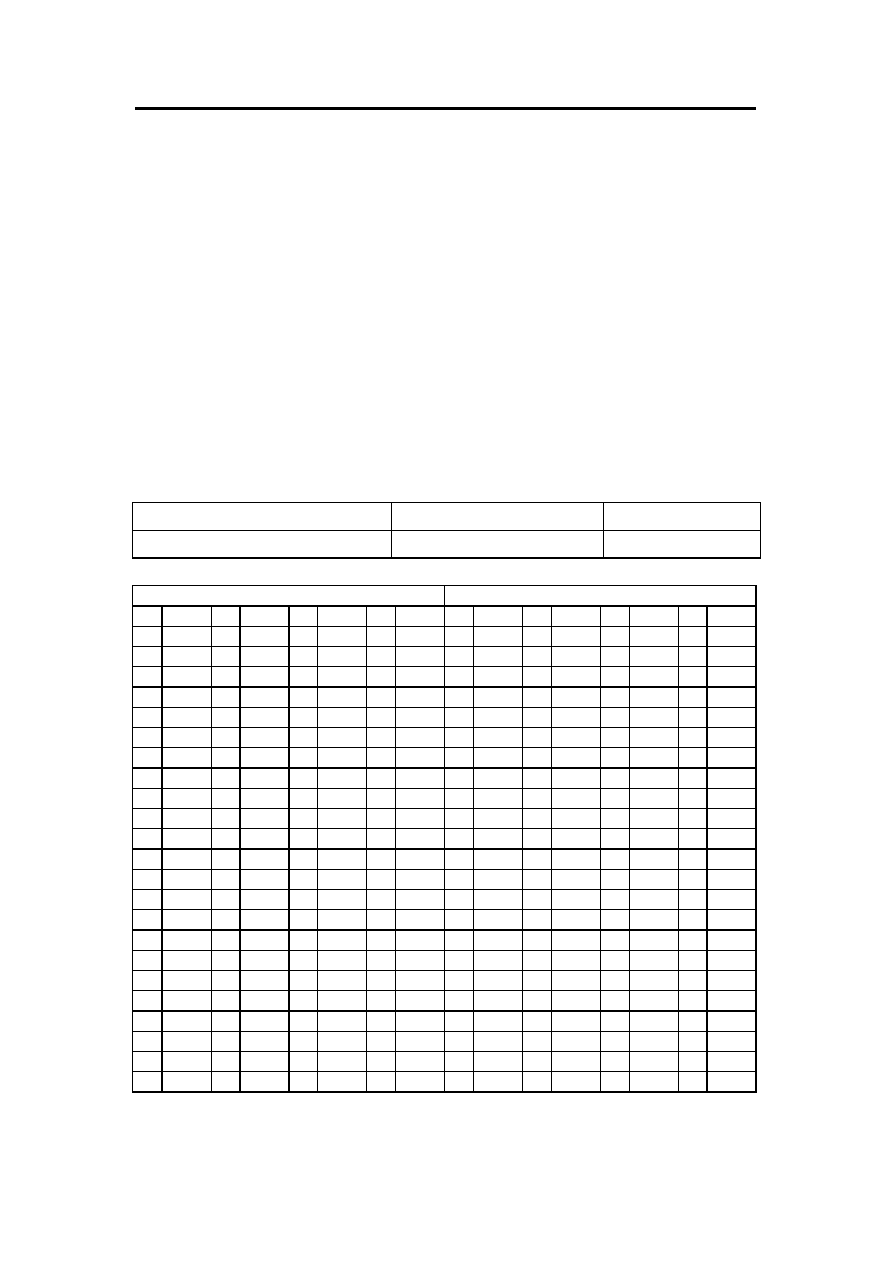
 | –≠–ª–µ–∫—Ç—Ä–æ–Ω–Ω—ã–π –∫–æ–º–ø–æ–Ω–µ–Ω—Ç: VDBDB1608 | –°–∫–∞—á–∞—Ç—å:  PDF PDF  ZIP ZIP |

V-Data
VDBCB1916
Revision History
Revision 1 ( Dec. 2001 )
1.Fister release.
Revision 2 ( Apr. 2002 )
1. Changed module current specification.
2. Add Performance range.
3.
Changed AC Characteristics.
4. Changed typo size on module PCB in package dimensions.
Rev 2 Apr. 2002
1
V-Data
VDBCB1916
DDR SDRAM 184pin DIMM
64Mx64bits DDR SDRAM 184pin DIMM based on 32Mx8
Performance range
General Description
The VDBCB1916 is 64Mx64 bits Double Data Rate
SDRAM Modules, The modules are composed of
sixteen 32Mx8 bits CMOS Double Data Rate
SDRAMs in TSOP-II 400mil 66pin package and one
2Kbit EEPROM in 8pin TSSOP(TSOP) package on a
184pin glass≠epoxy printed circuit board.
The V-Data is a Dual In-line Memory Module and is
intended for mounting onto 184-pins edge connector
sockets. Synchronous design allows precise cycle
control with the use of system clock. Data I/O
transactions are possible on both edges of DQS.
Range of operating frequencies, programmable
latencies and burst lengths allow the same device to
be useful for a variety of high bandwidth, high
performance memory system applications.
Features
∑
DLL aligns DQ and DQS transition with CK
transition
∑
Double-data-rate architecture.
∑
Bi-directional data strobe (DQS)
∑
Differential clock inputs(CK and /CK)
∑
Auto refresh and self refresh
∑
8192 refresh cycles / 64ms
∑
Power supply: Vdd,Vddq:2.5V±0.2V
∑
Programmable Burst length (2,4,8)
∑
Serial Presence Detect with EEPROM
∑
Module bank : two physical bank
∑
PCB : BUDA84A,Height (29.21mm),double
sided component, Six layers
Part No.
Max Freq.
Interface
VDBCB1916 133MHz
SSTL_2
Pin Assignment
FRONT SIDE
BACK SIDE
PIN NAME PIN
NAME
PIN
NAME
PIN NAME PIN NAME PIN NAME PIN NAME
PIN
NAME
1 VREF 24 DQ17 47 *DQS8 70
VDD
93
VSS 116 VSS 139 VSS 162 DQ47
2 DQ0 25
DQS2
48 A0 71 */CS2 94
DQ4 117 DQ21 140 *DM8
163
*/CS3
3 VSS 26 VSS 49 *CB2 72 DQ48 95
DQ5 118
A11
141
A10 164
VDDQ
4 DQ1 27 A9 50 VSS 73 DQ49 96 VDDQ 119 DM2 142 *CB6 165 DQ52
5 DQS0 28 DQ18 51 *CB3 74
VSS
97
DM0 120 VDD 143 VDDQ
166 DQ53
6 DQ2 29 A7 52 BA1 75
/CK2
98
DQ6 121 DQ22 144 *CB7 167 NC
7 VDD 30 VDDQ 53 DQ32 76
CK2
99
DQ7 122
A8 145 VSS 168 VDD
8 DQ3 31 DQ19 54 VDDQ 77 VDDQ 100 VSS 123 DQ23 146 DQ36 169 DM6
9 NC 32 A5 55 DQ33 78 DQS6 101
NC 124 VSS 147 DQ37 170 DQ54
10 NC 33
DQ24
56
DQS4
79 DQ50 102
NC 125
A6 148 VDD
171
DQ55
11 VSS 34 VSS 57 DQ34 80 DQ51 103 *A13 126 DQ28 149 DM4 172 VDDQ
12 DQ8 35 DQ25 58 VSS 81
VSS 104 VDDQ 127 DQ29 150 DQ38 173 NC
13 DQ9 36 DQS3 59 BA0 82 VDDID 105 DQ12 128 VDDQ 151 DQ39
174
DQ60
14 DQS1 37 A4 60 DQ35 83 DQ56 106 DQ13 129 DM3 152 VSS 175 DQ61
15 VDDQ 38 VDD 61 DQ40 84 DQ57 107 DM1 130
A3 153 DQ44 176 VSS
16 CK1 39 DQ26 62 VDDQ 85
VDD 108 VDD 131 DQ30 154 /RAS 177 DM7
17 /CK1 40 DQ27 63 /WE 86 DQS7 109 DQ14 132 VSS 155 DQ45
178
DQ62
18 VSS 41 A2 64 DQ41 87 DQ58 110 DQ15 133 DQ31 156 VDDQ 179 DQ63
19 DQ10 42 VSS 65 /CAS 88 DQ59 111 *CKE1 134 *CB4 157 /CS0 180 VDDQ
20 DQ11 43 A1 66 VSS 89
VSS 112 VDDQ 135 *CB5 158 */CS1 181 SA0
21 CKE0 44 *CB0 67 DQS5 90
NC 113 *BA2 136 VDDQ 159 DM5 182 SA1
22 VDDQ 45 *CB1 68 DQ42 91
SDA 114 DQ20 137 CK0 160 VSS 183 SA2
23 DQ16 46 VDD 69 DQ43 92
SCL
115
A12
138 /CK0 161 DQ46 184 VDDS
*
These pins are not used in this module.
Rev 2 Apr. 2002
2
V-Data
VDBCB1916
Pin Description
PIN NAME
FUNCTION
CK0~2,/CK0~2 System Clock
Active on the positive edge to sample all inputs.
CKE0~1 Clock
Enable
Masks system clock to freeze operation from the next clock cycle. CKE
should be enabled at least on cycle prior new command. Disable input
buffers for power down in standby
/CS0~3
Chip Select
Disables or Enables device operation by masking or enabling all input
except CK, CKE and L(U)DQM
A0~A12
Address
Row / Column address are multiplexed on the same pins.
BA0~BA1
Banks Select
Selects bank to be activated during row address latch time.
Selects bank for read / write during column address latch time.
DQ0~DQ63 Data
Data inputs / outputs are multiplexed on the same pins.
DQS0~DQS7 Data Strobe
Bi-directional Data Strobe
DQM0~7
Data Mask
Makes data output Hi-Z,
/RAS
Row Address Strobe
Latches row addresses on the positive edge of the CLK with /RAS low
/CAS
Column Address Strobe
Latches Column addresses on the positive edge of the CLK with /CAS
low
/WE
Write Enable
Enables write operation and row recharge.
VDD/VSS
Power Supply/Ground
Power and Ground for the input buffers and the core logic.
VDDQ
Power Supply
Power Supply for DQS
VREF
Power Supply reference
Power Supply for reference
VDDS
SPD Power Supply
Serial EEPROM power Supply
SDA
Serial data I/O
EEPROM serial data I/O
SCL
Serial clock
EEPROM clock input
SA0~2 Address
in EEPROM
EEPROM address input
VDDID
VDD identification
VDD identification flag
NC
No Connection
This pin is recommended to be left No Connection on the device.
Rev 2 Apr. 2002
3
V-Data
VDBCB1916
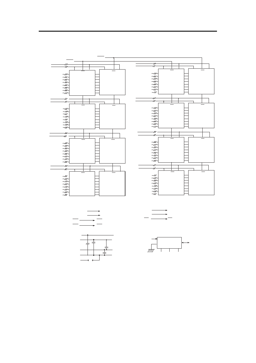
Block Diagram
DQ4
DQ5
DQ6
DQ7
DQ0
DQ1
DQ2
DQ3
DM
I/O 7
I/O 6
I/O 1
I/O 0
D0
DM0
DM
D8
I/O 5
I/O 4
I/O 3
I/O 2
I/O 0
I/O 1
I/O 6
I/O 7
I/O 2
I/O 3
I/O 4
I/O 5
DQ12
DQ13
DQ14
DQ8
DQ9
DQ10
DQ11
DM
I/O 7
I/O 6
I/O 1
I/O 0
D1
DM
D9
I/O 5
I/O 4
I/O 3
I/O 0
I/O 1
I/O 6
I/O 7
I/O 2
I/O 3
I/O 4
DM1
DQ20
DQ21
DQ22
DQ23
DQ16
DQ17
DQ18
DQ19
DM
I/O 7
I/O 6
I/O 1
I/O 0
D2
DM
D10
I/O 5
I/O 4
I/O 3
I/O 2
I/O 0
I/O 1
I/O 6
I/O 7
I/O 2
I/O 3
I/O 4
I/O 5
DM2
DQ28
DQ29
DQ30
DQ31
DQ24
DQ25
DQ26
DQ27
DM
I/O 7
I/O 6
I/O 1
I/O 0
D3
DM
D11
I/O 5
I/O 4
I/O 3
I/O 2
I/O 0
I/O 1
I/O 6
I/O 7
I/O 2
I/O 3
I/O 4
I/O 5
DM3
DQ36
DQ37
DQ38
DQ39
DQ32
DQ33
DQ34
DQ35
DM
I/O 7
I/O 6
I/O 1
I/O 0
D4
DM4
DM
D12
I/O 5
I/O 4
I/O 3
I/O 2
I/O 0
I/O 1
I/O 6
I/O 7
I/O 2
I/O 3
I/O 4
I/O 5
DQ44
DQ45
DQ46
DQ47
DQ40
DQ41
DQ42
DQ43
DM
I/O 7
I/O 6
I/O 1
I/O 0
D5
DM
D13
I/O 5
I/O 4
I/O 3
I/O 2
I/O 0
I/O 1
I/O 6
I/O 7
I/O 2
I/O 3
I/O 4
I/O 5
DM5
DQ52
DQ53
DQ54
DQ55
DQ48
DQ49
DQ50
DQ51
DM
I/O 7
I/O 6
I/O 1
I/O 0
D6
DM
D14
I/O 5
I/O 4
I/O 3
I/O 2
I/O 0
I/O 1
I/O 6
I/O 7
I/O 2
I/O 3
I/O 4
I/O 5
DQ60
DQ61
DQ62
DQ63
DQ56
DQ57
DQ58
DQ59
DM
I/O 7
I/O 6
I/O 1
I/O 0
D7
DM
D15
I/O 5
I/O 4
I/O 3
I/O 2
I/O 0
I/O 1
I/O 6
I/O 7
I/O 2
I/O 3
I/O 4
I/O 5
DM7
A0 - A13
A0-A13: SDRAMs D0 - D15
A0
Serial PD
A1
A2
SA0
SA1
SA2
SCL
SDA
RAS
RAS: SDRAMs D0 - D15
CAS
CAS: SDRAMs D0 - D15
CKE0
CKE: SDRAMs D0 - D7
WE
WE: SDRAMs D0 - D15
CS0
CS1
CS
CS
CS
CS
CS
CS
CS
CS
CS
CS
CS
CS
CS
CS
CS
CS
CKE1
CKE: SDRAMs D8 - D15
BA0 - BA1
BA0-BA1: SDRAMs D0 - D15
DQS0
DQS
DQS4
DQS1
DQS5
DQS
DQS
DQS2
DQS
DQS
DQS3
DQS
DQS
DM6
DQS6
DQS7
DQ15
I/O 2
I/O 5
DQS
DQS
DQS
DQS
DQS
DQS
DQS
DQS
DQS
V
SS
D0 - D15
D0 - D15
V
DD
/V
DDQ
D0 - D15
D0 - D15
VREF
V
DDID
Strap: see Note 4
WP
V
DDSPD
SPD
Rev 2 Apr. 2002
4
V-Data
VDBCB1916
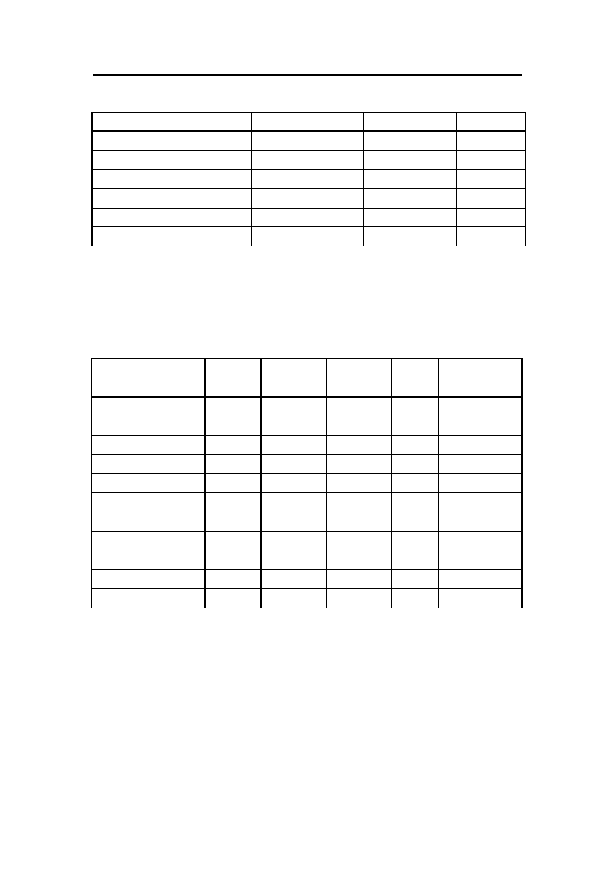
Absolute Maximum Ratings
Parameter Symbol
Value
Unit
Voltage on any pin relative to Vss
V
IN
, V
out
-0.5~3.6
V
Voltage on VDD supply relative to Vss
V
DD
-1.0~3.6
V
Voltage on VDDQ supply relative to Vss
V
DDQ
-0.5~3.6
V
Storage temperature
T
STG
-55~+150
Power dissipation
P
D
16
W
Short circuit current
I
OS
50
mA
Note : Permanent device damage may occur if ABSOLUTE MAXIMUM RATING are exceeded.
Functional operation should be restricted to recommended operating condition.
Exposure to higher than recommended voltage for extended periods of time could affect device reliability.
DC Operating Condition
Voltage referenced to Vss = 0V, T
A
= 0 to 70
Parameter Symbol
Min Max
Unit Note
Supply voltage
V
DD
, V
DDQ
2.3
2.7
V
Reference voltage
V
REF
V
DDQ
/2-50mV
V
DDQ
/2+50mV
V 1
Termination voltage
V
TT
V
REF-
0.04 V
REF
+0.04
2
Input logic high voltage
V
IH
V
REF
+0.15 V
DDQ
+0.3 V
3
Input logic low voltage
V
IL
-0.3
V
REF-
0.15 V
3
Output logic high voltage
V
OH
V
TT
+0.84 - V
I
OH
=-16.8mA
Output logic low voltage
V
OL
- V
TT-
0.84 V I
OL
=16.8mA
Input voltage Level
V
IN
-0.3
V
DDQ
+0.3 V
Input Differential Voltage
V
ID
0.3
V
DDQ
+0.6 V
4
Input crossing point voltage
V
IX
1.15 1.35 V
5
Input leakage current
I
IL
-2 2 uA
Output leakage current
I
OL
-5 5 uA
Note : 1. Includes±25mV margin for DC offset on V
REF
, and a combined total of ±50mV margin for all AC noise and
DC offset on V
REF
, bandwidth limited to 20MHz. The DRAM must accommodate DRAM current spikes on V
REF
and internal DRAM noise coupled TO V
REF
, both of which may result in V
REF
noise. V
REF
should be
de-coupled with an inductance of 3nH.
2.V
TT
is not applied directly to the device. V
TT
is a system supply for signal termination resistors, is expected
to be set equal to V
REF
, and must track variations in the DC level of V
REF
3.These parameters should be tested at the pin on actual components and may be checked at either the pin or
the pad in simulation. The AC and DC input specifications are relative to a VREF envelop that has been
bandwidth limited to 200MHz.
4.V
ID
is the magnitude of the difference between the input level on CK and the input level on /CK.
5.The value of V
IX
is expected to equal 0.5*V
DDQ
of the transmitting device and must track variations in the DC
level of the same.
Rev 2 Apr. 2002
5