
V-Data
VDD6632A4B
Revision History
Revision 1 ( Dec. 2001 )
1.Fister release.
Revision 2 ( Apr. 2002 )
1. Changed module current specification.
2. Add Performance range.
3.
Changed AC Characteristics.
4.
Changed typo size on module PCB in package dimensions.
Rev2 Apr, 2002
1
V-Data
VDD6632A4B
Double Data Rate SDRAM
512K x 32 Bit x 4 Banks
General Description
The VDD6632A4B are four-bank Double Data
Rate(DDR) Synchronous DRAMs organized as
2,097,152 words x 32 bits x 4 banks.
Synchronous design allows precise cycle control
with the use of system clock I/O transactions are
possible on every clock cycle.
Data outputs occur at both rising edges of CK and
/CK.
Range of operating frequencies, programmable
burst length and programmable latencies allow the
same device to be useful for a variety of high
bandwidth high performance memory system
applications
Features
�
2.5V for VDD power supply
�
SSTL_2 interface
�
MRS Cycle with address key programs
-CAS Latency (3)
-Burst Length (2,4)
-Burst Type (sequential & Interleave)
�
4 banks operation
�
Differential clock input (CK, /CK) operation
�
Double data rate interface
�
Auto & Self refresh
�
4096 refresh cycle
�
DQM for masking
�
Package:100-pins280mil LQFP
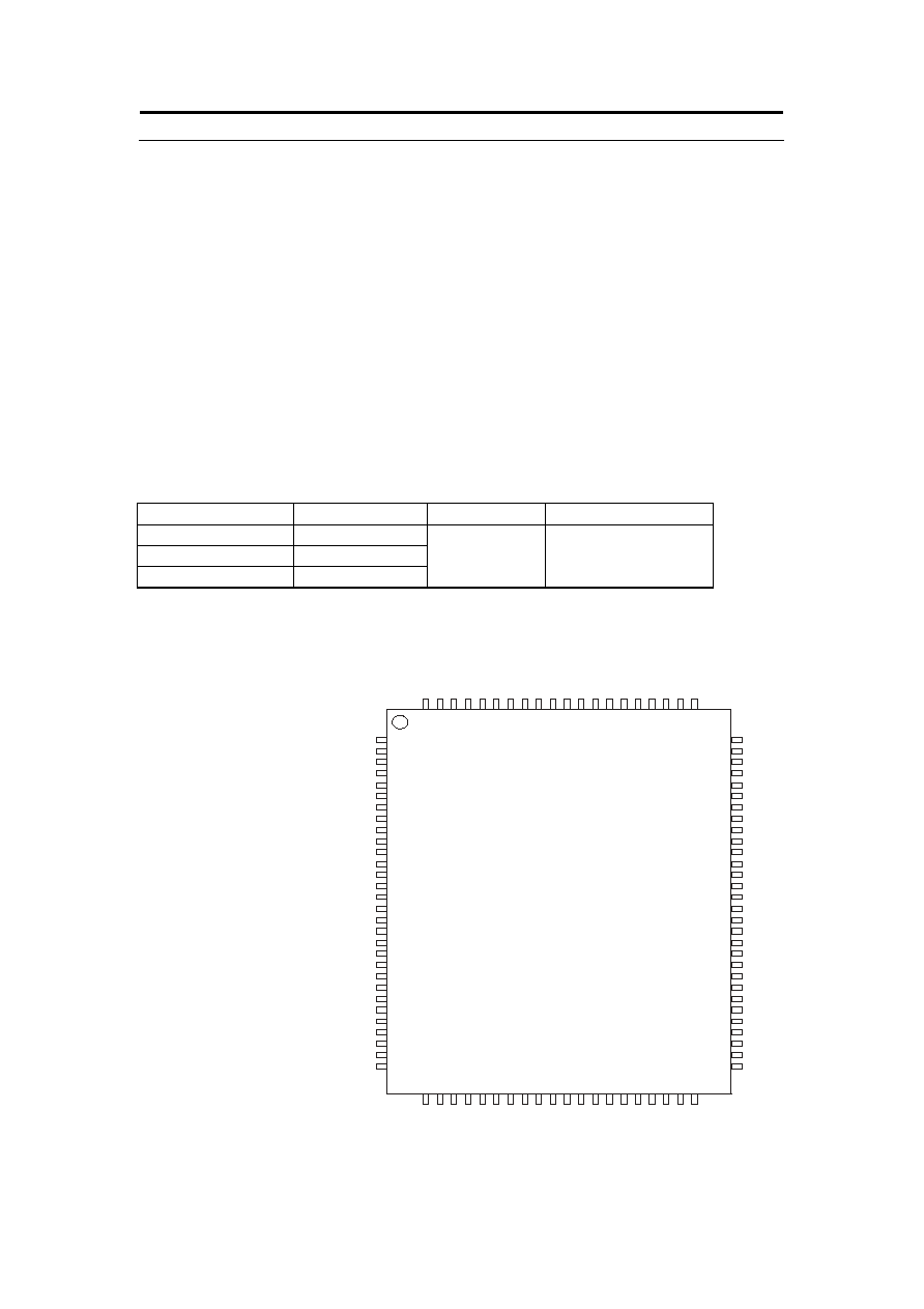
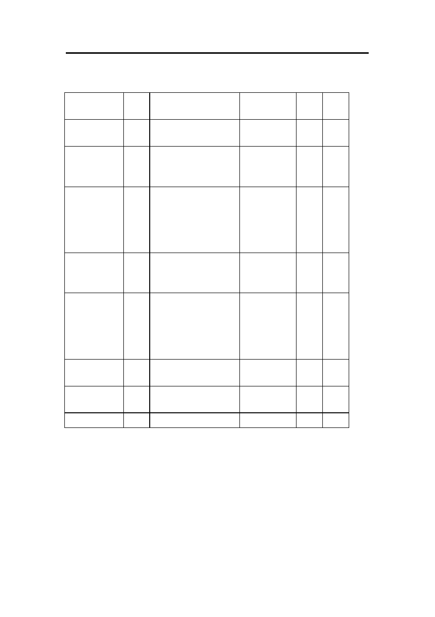
Ordering Information.
Part No.
Frequency
Interface
Package
VDD6632A4B-5 200Mhz
VDD6632A4B-5.5 183Mhz
VDD6632A4B-6 166Mhz
SSTL_2 100-pins
LQFP
Pin Assignment
DQ3
VDDQ
DQ4
DQ5
VSSQ
DQ6
DQ7
VDDQ
DQ16
DQ17
VSSQ
DQ18
DQ19
VDDQ
VDD
VSS
DQ20
DQ21
VSSQ
DQ22
DQ23
VDDQ
DM0
DM2
/WE
/CAS
/RAS
/CS
BA0
BA1
31
32
33
34
35
36
37
38
39
40
41
42
43
44
45
46
47
48
49
50
A0
A1
A2
A3
VDD
A10
NC
NC
NC
NC
NC
NC
NC
NC
A9
VSS
A4
A5
A6
A7
1
2
3
4
5
6
7
8
9
10
11
12
13
14
15
16
17
18
19
20
21
22
23
24
25
26
27
28
29
30
DQ28
VDDQ
DQ27
DQ26
VSSQ
DQ25
DQ24
VDDQ
DQ15
DQ14
VSSQ
DQ13
DQ12
VDDQ
VSS
VDD
DQ11
DQ10
VSSQ
DQ9
DQ8
VDDQ
VREF
DM3
DM1
CLK
/CLK
CKE
DSF, MCL
A8/AP
80
79
78
77
76
75
74
73
72
71
70
69
68
67
66
65
64
63
62
61
60
59
58
57
56
55
54
53
52
51
100
99
98
97
96
95
94
93
92
91
90
89
88
87
86
85
84
83
82
81
DQ2
VSSQ
DQ1
DQ0
VDD
VDDQ
DQS
NC
VSSQ
NC
NC
NC
NC
NC
VDDQ
VSS
DQ31 DQ30
VSSQ
DQ29
TOP VIEW
100-pin plastic LQFP 280 mil
Rev2 Apr, 2002
2
V-Data
VDD6632A4B
Pin Description
PIN NAME
FUNCTION
CK, /CK
System Clock
Differential clock input.
CKE Clock
Enable
Masks system clock to freeze operation from the next clock cycle. CKE
should be enabled at least on cycle prior new command. Disable input
buffers for power down in standby
/CS
Chip Select
Disables or Enables device operation by masking or enabling all input
except CK, CKE and L(U)DQM
A0~A10
Address
Row / Column address are multiplexed on the same pins.
Row address : A0~A10
Column address : A0~A7
BA0~BA1 Banks Select
Selects bank to be activated during row address latch time.
Selects bank for read / write during column address latch time.
DQ0~DQ31 Data
Data inputs / outputs are multiplexed on the same pins.
L(U)DQM Data Mask
Makes data output Hi-Z,
LDQS,UDQS Data Strobe
Bi-directional Data Strobe.
/RAS
Row Address Strobe
Latches row addresses on the positive edge of the CLK with /RAS low
/CAS
Column Address Strobe
Latches Column addresses on the positive edge of the CLK with /CAS
low
/WE
Write Enable
Enables write operation and row recharge.
VDD/VSS Power Supply/Ground
Power and Ground for the input buffers and the core logic.
V
DDQ
/V
SSQ
Data Output Power/Ground Power supply for output buffers.
VREF
Reference Voltage
Reference voltage for inputs for SSTL interface.
NC
No Connection
This pin is recommended to be left No Connection on the device.
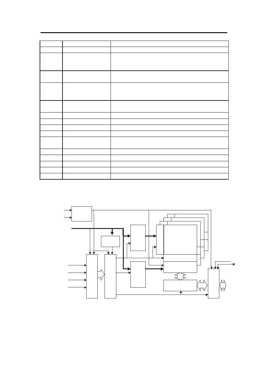
Block Diagram
CK
CKE
Clock
Generator
Address
/CS
/RAS
/CAS
/WE
DQM
Mode
Register
Command Decoder
Control Logic
Row Decoder
Address
Buffer
&
Refresh
Counter
Column
Address
Buffer
&
Refresh
Counter
Bank0
Bank2
Bank3
Bank1
Amplifier
Column Decoder
Data Control Circuit
Data Latch
DQ0~DQn
DQS
Rev2 Apr, 2002
3
V-Data
VDD6632A4B
Absolute Maximum Ratings
Parameter Symbol
Value
Unit
Voltage on any pin relative to Vss
V
IN
, V
out
-0.3 ~ VDD+0.3
V
Voltage on VDD supply relative to Vss
V
DD
, V
DDQ
-0.3
~
4.6
V
Storage temperature
T
STG
-55 ~ +150
Power dissipation
P
D
1
W
Short circuit current
I
OS
50
mA
Note : Permanent device damage may occur if ABSOLUTE MAXIMUM RATING are exceeded.
Functional operation should be restricted to recommended operating condition.
Exposure to higher than recommended voltage for extended periods of time could affect device reliability.
DC Operating Condition
Voltage referenced to Vss = 0V, T
A
= 0 to 70
Parameter Symbol
Min
Max
Unit
Note
Supply voltage
V
DD
2.5 2.7
V
Supply voltage
V
DDQ
2.5 2.7 1
Input logic high voltage
V
IH
V
REF
+0.18
V
DDQ
+0.3 V
Input logic low voltage
V
IL
-0.3
V
REF
-0.18
V 2
Output logic high voltage
V
OH
V
TT
+0.75 - V
I
OH
=-15.2mA
Output logic low voltage
V
OL
-
V
TT
-0.75 V I
OL
=15.2mA
Input leakage current
I
IL
-5 5
uA
3
Output leakage current
I
OL
-5 5
uA
4
Reference Voltage
V
REF
1.25 1.35 V
Termination Voltage
V
TT
V
REF
-0.04
V
REF
+0.04
5
Note : 1. V
DDQ
must not exceed the level of V
DDQ
.
2.V
IL
(min)=-1.5V AC for pulse width 5ns acceptable.
3.Any
input
0V
V
IN
3.6V, all other pins are not under test = 0V.
4.Dout is disabled, 0V V
OUT
2.7V.
5.
V
REF
is expected to be equal to 0.5* V
DDQ
of the transmitting device, and to track variations in the DC level of
the same. Peak to peak noise on V
REF
may not exceed �2% of the DC value.
Rev2 Apr, 2002
4
V-Data
VDD6632A4B
AC Operating Condition
Voltage referenced to Vss = 0V, T
A
= 0 to 70
Parameter Symbol
Value
Unit
Note
AC input high / low level voltage
V
IH
/ V
IL
2.4 / 0.4
V
Input timing measurement reference level voltage
Vtrip
1.4
V
Input rise / fall time
TR / tF
1
Ns
Output timing measurement reference level
Voutfef
1.4
V
Output load capacitance for access time measurement
CL
50
pF
2
Note: 1. 3.15V V
DD
3.6V is applied for VDD6632A4B5.
2. Output load to measure access times is equivalent to two TTL gates and one capacitor (30pF). For details,
refer to AC/DC output load circuit.
Capacitance
TA=25, f-=1Mhz
Parameter Pin
Symbol
Min
Max
Unit
CK, /CK
Cl1
2.5
3.5
pF
Input capacitance
A0~A11,BA0,BA1,CKE,/CS,/RAS,
/CAS,/WE,DQM
Cl2 2.5
3.5
pF
Data input / output capacitance DQM
CI/O
4.0
5.5
pF
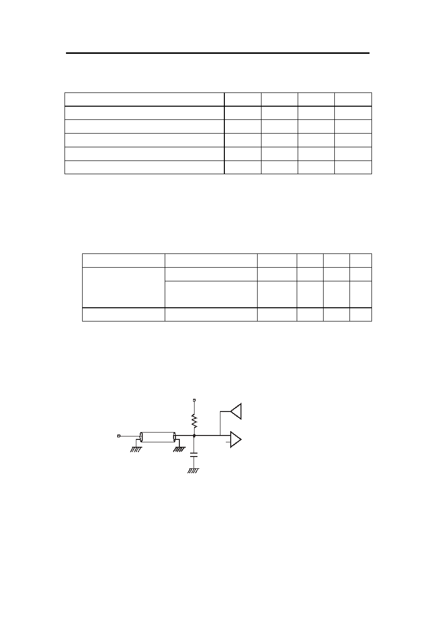
Output load circuit
Output Load Circuit (SSTL_2)
Output
Z0=50
C
LOAD
=30pF
V
REF
=0.5*V
DDQ
R
T
=50
V
tt
=0.5*V
DDQ
Rev2 Apr, 2002
5
V-Data
VDD6632A4B
DC Characteristics II
Parameter Symbol
Test
condition
MAX
Unit
Note
Operating Current
IDD1
Burst length=2, One bank active
tRCtRC(min),I
OL
=0mA
165 mA
1
Precharge standby
current in power
down mode
IDD2P
CKEV
IL
(max), tCK=min
2 mA
Precharge standby
current in Non power
down mode
IDD2N
CKEV
IH
(min), /CSV
IH
(min),
tCK=min input signals are
changed one time during 2clks.
All other pins VDD-0.2V or
0.2V
60 mA
Active standby
current in power
down mode
IDD3P
CKEV
IL
(max), tCK=min
5 mA
Active standby
current in Non power
down mode
IDD3N
CKEV
IH
(min), /CSV
IH
(min),
tCK=min input signals are
changed one time during 2clks.
All other pins VDD-0.2V or
0.2V
130 mA
Burst mode operating
current
IDD4
t
CK
t
CK
(min),I
OL
=0 mA
All banks active
240 mA
1
Auto refresh current IDD5
tRRCtRRC(min), All banks
active
160 mA
2
Self refresh current
IDD6
CKE0.2V
2 mA
Note: 1. IDD1 and IDD4 depend on output loading and cycle rates. Specified values are measured with the output
open.
2. Min. of tRRC is shown at AC characteristics.
Rev2 Apr, 2002
6
V-Data
VDD6632A4B
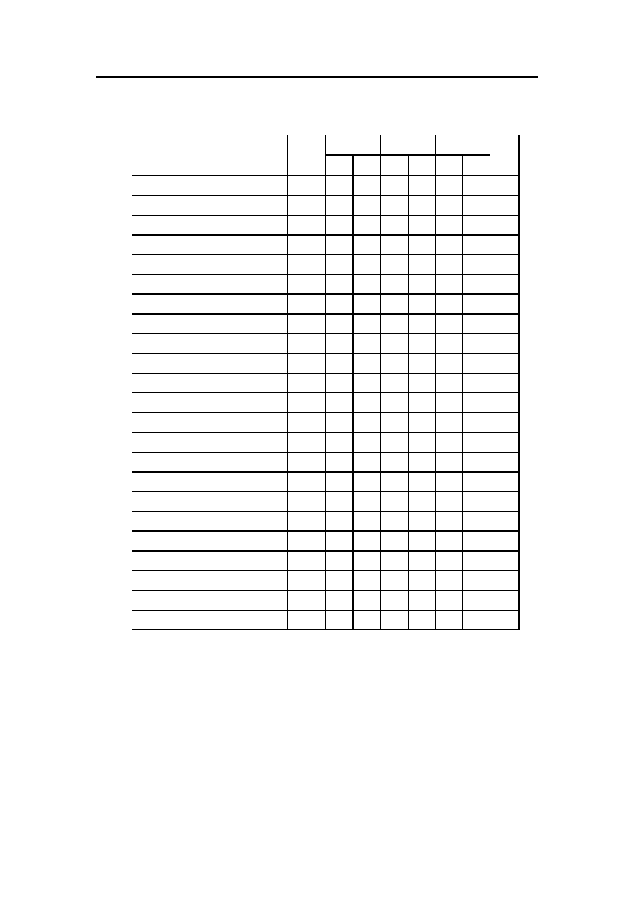
AC Characteristics
-5 -5.5 -6
Parameter Symbol
Min
Max
Min
Max
Min Max
Unit
System clock Cycle time
tCK
5
8
5.5
8
6
8
ns
Clock high pulse width
tCHW
0.45
0.55
0.45
0.55
0.45 0.55 CLK
Clock low pulse width
tCLW
0.45
0.55
0.45
0.55
0.45 0.55 CLK
Access time form CK to /CK
tAC
-0.1-
0.1
-0.1
0.1
-0.1
0.1
CLK
Data strobe edge to clock edge
tDQSCK -0.1-
0.1
-0.1
0.1
-0.1
0.1
ns
Clock to first rising edge of DQS delay
tDQSS
0.75
1.25
0.75
1.25
0.75 1.25 CLK
/RAS cycle time
tRC
55
-
60.5
-
60
-
ns
/RAS to /CAS delay
tRCD
15
-
16.5
-
18
-
ns
/RAS active time
tRAS
35
120K
35
120K
42
120K
ns
/RAS precharge time
tRP
16
-
16.5
-
18
-
ns
/RAS to /RAS bank active delay
tRRD
10
-
11
-
12
-
ns
Data-in setup time (to DQS)
tDS
0.5
-
0.5
-
0.5
-
ns
Data-in hold time (to DQS)
tDH
1
1
-
1
-
ns
DQS input high pulse width
tDQSH
0.4
0.6
0.4
0.6
0.4
0.6
ns
DQS input low pulse width
tDQSL
0.4
0.6
0.4
0.6
0.4
0.6
ns
Input setup time
tIS
0.9
-
0.9
-
1.1
-
ns
Input hold time
tIH
0.9
-
0.9
-
1.1
-
ns
DQS-in high level width
tDSH
0.4
0.6
0.4
0.6
0.4
0.6
CLK
DQS-in low level width
tDSL
0.4
0.6
0.4
0.6
0.4
0.6
CLK
Write postamble
tWPST
0.4
0.6
0.4
0.6
0.4
0.6
CLK
Write
preamble
tWPRE
0.25
0.25
0.25 CLK
Data strobe edge to output data edge
tDQSQ
0.5
0.5
0.5
ns
DQS read preamble
tRPRE
0.9
1.1
0.9
1.1
0.9
1.1
CLK
Rev2 Apr, 2002
7
V-Data
VDD6632A4B
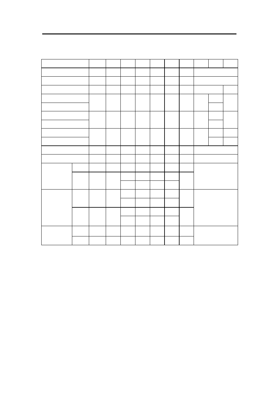
Command Truth-Table
Command CKEn-1
CKEn
/CS
/RAS
/CAS
/WE
DQM
ADDR
A8/AP
BA
Mode
Register
Set
H X L L L L X
OP
code
No
Operation
H X L H H H X
X
Bank Active
H
X
L
L
H
H
X
RA
V
Read
L
Read with Auto Precharge
H X L H L H X CA
H
V
Write
L
Write with Auto Precharge
H X L H L L X CA
H
V
Precharge All Bank
H X
Precharge select Bank
H X L L H L X X
L V
Burst
Stop
H X L H H L X
X
Auto
Refresh
H H L L L H X
X
Entry
H L L L L H X
H X X X
Self Refresh
Exit L H
L H H H
X
X
H X X X
Entry
H L
L H H H
X
H X X X
Precharge
Power down
Exit L H
L H H H
X
X
Entry
H L X X X X X
Clock Suspend
Exit L H X X X X X
X
Rev2 Apr, 2002
8

V-Data
VDD6632A4B
Package Information
E
H
y
A
A2
Seating Plane
L
L
1
See Detail F
A1
D
H
D
0.08
0
7
0
0.003
1.00
0.75
16.10
0.60
16.00
0.45
15.90
0.039
0.030
0.870
0.634
0.024
0.866
0.630
0.018
0.862
0.626
0.65
20.10
14.10
0.20
0.38
1.45
20.00
14.00
1.40
19.90
13.90
0.10
0.22
1.35
0.791
0.555
0.008
0.015
0.057
0.787
0.551
0.055
0.026
0.783
0.547
0.004
0.009
0.053
Symbol
Min Nom Max
Max
Nom
Min
Dimension in inch
Dimension in mm
A
b
c
D
e
H
D
H
E
L
y
A
A
L
1
1
2
E
0.013
0.006
0.15
0.32
21.90 22.00 22.10
7
0.020
0.032 0.498
0.802
0.10
0.05
0.002 0.004 0.006
0.15
280mil 100pin LQFP Package
Rev2 Apr, 2002
9