
Advanced Power
N-CHANNEL ENHANCEMENT MODE
Electronics Corp.
POWER MOSFET
SO-8 similar area footprint and pin assignment
BV
DSS
30V
Low Gate Drive Voltage
R
DS(ON)
4.2m
Lower On-resistance
I
D
75A
RoHS Compliant
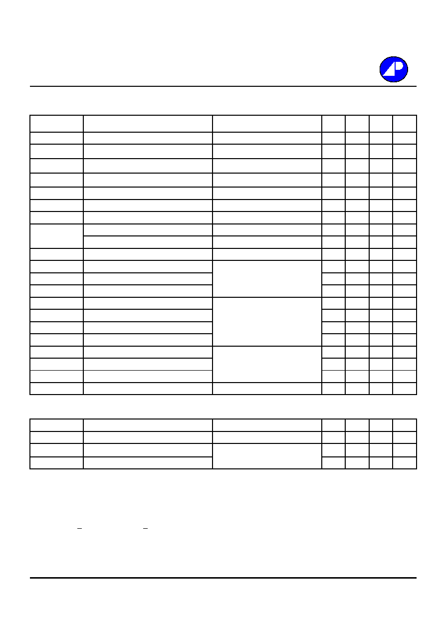
Description
Absolute Maximum Ratings
Symbol
Units
V
DS
V
V
GS
V
I
D
@T
C
=25
A
I
D
@T
C
=100
A
I
DM
A
P
D
@T
C
=25
W
W/
E
AS
Single Pulse Avalanche Energy
4
mJ
I
AR
Avalanche Current
A
T
STG
T
J
Symbol
Value
Units
Rthj-c
Thermal Resistance Junction-case
Max.
1.8
/W
Rthj-a
Thermal Resistance Junction-ambient
3
Max.
85
/W
Data & specifications subject to change without notice
29
24
30
Parameter
Operating Junction Temperature Range
Pulsed Drain Current
1
Total Power Dissipation
Linear Derating Factor
Storage Temperature Range
0.6
-55 to 150
200429052-1/4
Thermal Data
Parameter
Drain-Source Voltage
Continuous Drain Current, V
GS
@ 4.5V
Gate-Source Voltage
Continuous Drain Current, V
GS
@ 4.5V
70
-55 to 150
�12
75
56
300
AP0503GMA
Rating
Pb Free Plating Product
The APAK-5 package is preferred for all commercial-industrial surface
mount applications and suited for low voltage applications such as
DC/DC converters.
G
D
S
S
S
S G
D
APAK-5
Electrical Characteristics@T
j
=25
o
C(unless otherwise specified)
Symbol
Parameter
Test Conditions
Min.
Typ. Max. Units
BV
DSS
Drain-Source Breakdown Voltage
V
GS
=0V, I
D
=250uA
30
-
-
V
B
V
DSS
/T
j
Breakdown Voltage Temperature Coefficient
Reference to 25
, I
D
=1mA
-
0.018
-
V/
R
DS(ON)
Static Drain-Source On-Resistance
2
V
GS
=10V, I
D
=30A
-
-
4.2
m
V
GS
=4.5V, I
D
=30A
-
-
6
m
V
GS
=2.5V, I
D
=20A
-
-
9
m
V
GS(th)
Gate Threshold Voltage
V
DS
=V
GS
, I
D
=250uA
0.5
-
1.2
V
g
fs
Forward Transconductance
V
DS
=5V, I
D
=30A
-
88
-
S
I
DSS
Drain-Source Leakage Current (T
j
=25
o
C)
V
DS
=30V, V
GS
=0V
-
-
1
uA
Drain-Source Leakage Current (T
j
=150
o
C)
V
DS
=24V, V
GS
=0V
-
-
25
uA
I
GSS
Gate-Source Leakage
V
GS
=�12V
-
-
�100
nA
Q
g
Total Gate Charge
2
I
D
=30A
-
52
83
nC
Q
gs
Gate-Source Charge
V
DS
=24V
-
8
-
nC
Q
gd
Gate-Drain ("Miller") Charge
V
GS
=4.5V
-
21
-
nC
t
d(on)
Turn-on Delay Time
2
V
DS
=15V
-
19
-
ns
t
r
Rise Time
I
D
=30A
-
83
-
ns
t
d(off)
Turn-off Delay Time
R
G
=3.3
,
V
GS
=5V
-
60
-
ns
t
f
Fall Time
R
D
=0.5
-
115
-
ns
C
iss
Input Capacitance
V
GS
=0V
-
5130 8200
pF
C
oss
Output Capacitance
V
DS
=25V
-
620
-
pF
C
rss
Reverse Transfer Capacitance
f=1.0MHz
-
360
-
pF
R
g
Gate Resistance
f=1.0MHz
-
0.85
1.3
Source-Drain Diode
Symbol
Parameter
Test Conditions
Min.
Typ. Max. Units
V
SD
Forward On Voltage
2
I
S
=45A, V
GS
=0V
-
-
1.3
V
t
rr
Reverse Recovery Time
2
I
S
=30A,
V
GS
=0
V
,
-
38
-
ns
Q
rr
Reverse Recovery Charge
dI/dt=100A/�s
-
30
-
nC
Notes:
1.Pulse width limited by safe operating area.
2.Pulse width <300us , duty cycle <2%.
3.Surface mounted on FR4 board.
4.Starting T
j
=25
o
C , V
DD
=25V , L=0.1mH , R
G
=25
2/4
AP0503GMA

AP0503GMA
Fig 1. Typical Output Characteristics
Fig 2. Typical Output Characteristics
Fig 3. On-Resistance v.s. Gate Voltage
Fig 4. Normalized On-Resistance
v.s. Junction Temperature
Fig 5. Forward Characteristic of
Fig 6. Gate Threshold Voltage v.s.
Reverse Diode
Junction Temperature
3/4
0.0
0.5
1.0
1.5
2.0
-50
0
50
100
150
T
j
, Junction Temperature (
o
C)
N
o
rmalize
d
V
GS(t
h)
(V
)
0
50
100
150
0
1
2
3
4
5
V
DS
, Drain-to-Source Voltage (V)
I
D
, Dr
a
i
n C
u
r
r
e
nt
(A
)
T
C
=25
o
C
V
G
=1.5V
5.0V
4.5V
3.5V
2.5V
0
50
100
150
0
1
2
3
4
5
V
DS
, Drain-to-Source Voltage (V)
I
D
, Dr
a
i
n C
u
r
r
e
nt
(A
)
V
G
= 1.5 V
5.0 V
4.5 V
3.5 V
2.5V
T
C
= 1 50
o
C
0.5
0.9
1.3
1.7
-50
0
50
100
150
T
j
, Junction Temperature (
o
C)
N
o
rmalize
d
R
DS(ON)
I
D
=30A
V
G
=4.5V
0
2
4
6
0
0.2
0.4
0.6
0.8
1
V
SD
, Source-to-Drain Voltage (V)
Is (
A
)
T
j
=25
o
C
T
j
=150
o
C
4
8
12
16
0
2
4
6
8
10
V
GS
, Gate-to-Source Voltage (V)
R
DS(ON)
(m
)
I
D
= 20 A
T
c
=25

AP0503GMA
Fig 7. Gate Charge Characteristics
Fig 8. Typical Capacitance Characteristics
Fig 9. Maximum Safe Operating Area
Fig 10. Effective Transient Thermal Impedance
Fig 11. Transfer Characteristics
Fig 12. Gate Charge Waveform
4/4
Q
V
G
4.5V
Q
GS
Q
GD
Q
G
Charge
100
1000
10000
1
6
11
16
21
26
31
V
DS
,Drain-to-Source Voltage (V)
C (
p
F)
f=1.0MHz
C
iss
C
oss
C
rss
0
3
6
9
12
15
0
30
60
90
120
150
Q
G
, Total Gate Charge (nC)
V
GS
,
G
a
te
to S
o
u
r
c
e
Voltage
(
V
)
V
DS
=15V
V
DS
=20V
V
DS
=24V
I
D
=30A
1
10
100
1000
0.1
1
10
100
V
DS
, Drain-to-Source Voltage (V)
I
D
(A
)
T
c
=25
o
C
Single Pulse
1ms
10ms
100ms
DC
0
20
40
60
80
100
0
1
2
3
4
V
GS
, Gate-to-Source Voltage (V)
I
D
, Dr
a
i
n C
u
r
r
e
nt
(A
)
T
j
=150
o
C
T
j
=25
o
C
V
DS
=5V
0.01
0.1
1
0.00001
0.0001
0.001
0.01
0.1
1
t , Pulse Width (s)
N
o
rmalize
d
T
h
e
r
mal Re
spon
se
(
R
th
jc
)
P
DM
Duty factor = t/T
Peak T
j
= P
DM
x R
thjc
+ T
C
t
T
0.02
0.01
0.05
0.1
0.2
Duty factor=0.5
Single Pulse