Advanced Power
N-CHANNEL INSULATED GATE
Electronics Corp.
BIPOLAR TRANSISTOR
Description
V
CES
I
CP
* High Input Impedance
* High Pick Current Capability
* 4.5V Gate Drive
* Strobe Flash Applications
Absolute Maximum Ratings
Electrical Characteristics@T
j
=25
o
C(unless otherwise specified)
Symbol
Min.
Typ.
Max. Units
I
GES
-
-
10
uA
I
CES
-
-
10
uA
V
CE(sat)
-
5
8
V
V
GE(th)
-
-
1.2
V
Q
g
-
51
-
nC
Q
ge
-
2
-
nC
Q
gc
-
5.4
-
nC
t
d(on)
-
5.5
-
ns
t
r
-
72
-
ns
t
d(off)
-
640
-
ns
t
f
-
2.6
-
us
C
ies
-
2095
-
pF
C
oes
-
145
-
pF
C
res
-
35
-
pF
Rthj-c
-
-
6
/W
Data and specifications subject to change without notice
V
20
200124032
V
CC
=200V
V
Gate-Emitter Voltage
Gate-Emitter Charge
Operating Junction Temperature Range
-55 to 150
-55 to 150
W
Parameter
Storage Temperature Range
Pulsed Collector Current
Parameter
Maximum Power Dissipation
V
GE
I
CP
I
GEP
Pulsed Gate-Emitter Voltage
P
D
@T
C
=25
450
� 6
130
� 8
AP20G45EH/J
Symbol
V
CES
450V
130A
Rating
Collector-Emitter Voltage
Units
V
A
Reverse Transfer Capacitance
V
CE
=450V, V
GE
=0V
V
GE
=4.5V, I
CP
=130A (Pulsed)
V
CE
=V
GE
, I
C
=250uA
I
C
=40A
V
CE
=300V
V
GE
=5V
V
CE
=25V
Test Conditions
Collector-Emitter Saturation Voltage
Gate Threshold Voltage
Total Gate Charge
Gate-Emitter Leakage Current
Collector-Emitter Leakage Current (Tj=25
)
V
GE
=6V, V
CE
=0V
T
STG
Turn-off Delay Time
V
GE
=0V
I
C
=40A
R
G
=25
Rise Time
T
J
Gate-Collector Charge
Turn-on Delay Time
V
GE
=5V
Thermal Resistance Junction-Case
Fall Time
Input Capacitance
Output Capacitance
f=1.0MHz
G
C
E
TO-252(H)
G
C
E
TO-251(J)
G
C
E

Fig 1. Typical Output Characteristics
Fig 2. Typical Output Characteristics
Fig 3. Collector Current v.s.
Fig 4. Collector- Emitter Saturation Voltage
Gate-Emitter Voltage
v.s. Case Temperature
AP20G45EH/J
0
40
80
120
160
0
2
4
6
8
10
12
V
CE
, Collector Emitter Voltage (V)
I
C
, Collector Cu
rren
t
(
A
)
T
C
=25
o
C
V
G
=5.0V
V
G
=4.5V
V
G
=4.0V
V
G
=3.0V
V
G
=2.0V
V
G
=1.0V
0
40
80
120
0
2
4
6
8
10
12
V
CE
, Collector-Emitter Voltage (V)
I
C
, Collector Cu
rren
t
(
A
)
T
C
=150
o
C
V
G
=5.0V
V
G
=4.5V
V
G
=4.0V
V
G
=3.0V
V
G
=2.0V
V
G
=1.0V
0
40
80
120
160
0
1
2
3
4
5
6
V
GE
, Gate- Emitter Voltage (V)
I
C
, Collector Cu
rren
t
(
A
)
T
C
=25
o
C
T
C
=70
o
C
T
C
=100
o
C
T
C
=150
o
C
V
CE
=8V
0
2
4
6
8
10
12
0
20
40
60
80
100
120
140
160
T
C
, Case Temperature (
o
C )
V
CE(s
a
t
)
, S
a
tu
r
a
tion
Voltage (
V
)
I
C
= 130A
I
C
= 100A
I
C
= 70A
I
C
= 35A
V
GE
= 4.5 V
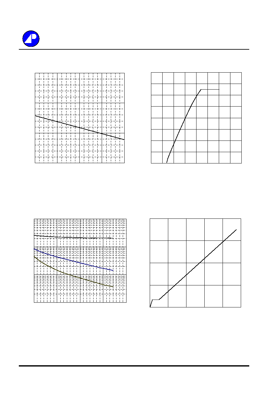
Fig 5. Gate-Emitter Cut-Off Voltage
Fig 6. Safe Operation Area
v.s. Case Temperature
Fig 7. Collector v.s. Collector-Emitter Voltage Fig 8. Gate Charge Waveform
AP20G45EH/J
0
0.5
1
1.5
-50
0
50
100
150
T
C
, Case Temperature (
o
C )
V
GE
(
t
h
)
G
a
te T
h
r
e
s
h
old Voltage (
V
)
0
2
4
6
8
0
15
30
45
60
75
Q
G
, Gate Charge (nC)
V
GE
, G
a
te-
E
m
i
tter
Voltage (
V
)
I
CP
=40A
V
CE
=300V
0
40
80
120
160
0
2
4
6
8
V
GE
, Gate-Emitter Voltage (V)
I
CP
, P
e
ak Collector
Cu
r
r
e
n
t
(
A
)
V
G
=4.5V
T
C
= 25
o
C
10
100
1000
10000
1
8
15
22
29
V
CE
, Collector-Emitter Voltage (V)
Capacitan
ce (
p
F)
f=1.0MHz
Cies
Cies
Cies
Cies
Coes
Coes
Coes
Coes
Cres
Cres
Cres
Cres

Fig 9. Switching Time Test Circuit
Fig 10. Switching Time Waveform
Fig 11. Gate Charge Test Circuit
Fig 12. Application Test Circuit
AP20G45EH/J
t
d(on)
t
r
t
d(off)
t
f
V
CE
V
GE
10%
90%
V =200V
TO THE
OSCILLOSCOPE
-
+
5 V
C
G
E
V
CE
V
GE
R
R
C
G
CC
300V
TO THE
OSCILLOSCOPE
-
+
C
G
V
CE
V
GE
I
C
I
G
1~3 mA
E
V
CM
V
CM
= 300V
C
M
= 160uF
I
CP
= 130A
V
G
= 5V
+
_
C
M
R
G
V
trig
IGBT
V
G
Flasher