Advanced Power
N-CHANNEL ENHANCEMENT MODE
Electronics Corp.
POWER MOSFET
Fast Switching Characteristic
BV
DSS
30V
Lower Gate Charge
R
DS(ON)
45m
Small Footprint & Low Profile Package
I
D
5.5A
RoHS Compliant
Description
Absolute Maximum Ratings
Symbol
Units
V
DS
V
V
GS
V
I
D
@T
A
=25
A
I
D
@T
A
=70
A
I
DM
A
P
D
@T
A
=25
W
W/
T
STG
T
J
Symbol
Value
Unit
Rthj-a
Thermal Resistance Junction-ambient
3
Max.
62.5
/W
Data and specifications subject to change without notice
Thermal Data
Parameter
Storage Temperature Range
Total Power Dissipation
2
-55 to 150
Operating Junction Temperature Range
-55 to 150
Linear Derating Factor
0.016
Continuous Drain Current
3
, V
GS
@ 4.5V
4.4
Pulsed Drain Current
1
20
Gate-Source Voltage
Continuous Drain Current
3
, V
GS
@ 4.5V
5.5
Parameter
Rating
Drain-Source Voltage
30
200517051-1/4
AP2604GY
Pb Free Plating Product
�20
G
D
S
Advanced Power MOSFETs utilized advanced processing techniques
to achieve the lowest possible on-resistance, extremely efficient and
cost-effectiveness device.
The S0T-26 package is universally used for all commercial-industrial
applications.
D
D
D
D
G
S
SOT-26
Electrical Characteristics@T
j
=25
o
C(unless otherwise specified)
Symbol
Parameter
Test Conditions
Min.
Typ. Max. Units
BV
DSS
Drain-Source Breakdown Voltage
V
GS
=0V, I
D
=250uA
30
-
-
V
B
V
DSS
/T
j
Breakdown Voltage Temperature Coefficient
Reference to 25
, I
D
=1mA
-
0.02
-
V/
R
DS(ON)
Static Drain-Source On-Resistance
2
V
GS
=10V, I
D
=4.8A
-
-
45
m
V
GS
=4.5V, I
D
=2.4A
-
-
65
m
V
GS(th)
Gate Threshold Voltage
V
DS
=V
GS
, I
D
=250uA
1
-
3
V
g
fs
Forward Transconductance
V
DS
=10V, I
D
=4.8A
-
7
-
S
I
DSS
Drain-Source Leakage Current (T
j
=25
o
C)
V
DS
=30V, V
GS
=0V
-
-
1
uA
Drain-Source Leakage Current (T
j
=70
o
C)
V
DS
=24V ,V
GS
=0V
-
-
25
uA
I
GSS
Gate-Source Leakage
V
GS
=
-
-
nA
Q
g
Total Gate Charge
2
I
D
=4.8A
-
6
10
nC
Q
gs
Gate-Source Charge
V
DS
=24V
-
2
-
nC
Q
gd
Gate-Drain ("Miller") Charge
V
GS
=4.5V
-
3
-
nC
t
d(on)
Turn-on Delay Time
2
V
DS
=15V
-
6
-
ns
t
r
Rise Time
I
D
=1A
-
8
-
ns
t
d(off)
Turn-off Delay Time
R
G
=3.3
,
V
GS
=10V
-
15
-
ns
t
f
Fall Time
R
D
=15
-
4
-
ns
C
iss
Input Capacitance
V
GS
=0V
-
440
705
pF
C
oss
Output Capacitance
V
DS
=25V
-
105
-
pF
C
rss
Reverse Transfer Capacitance
f=1.0MHz
-
35
-
pF
Source-Drain Diode
Symbol
Parameter
Test Conditions
Min.
Typ. Max. Units
V
SD
Forward On Voltage
2
I
S
=4.8A, V
GS
=0V
-
-
1.2
V
t
rr
Reverse Recovery Time
2
I
S
=4.8A, V
GS
=0V,
-
15
-
ns
Q
rr
Reverse Recovery Charge
dI/dt=100A/�s
-
7
-
nC
Notes:
1.Pulse width limited by Max. junction temperature.
2.Pulse width <300us , duty cycle <2%.
3.Surface mounted on 1 in
2
copper pad of FR4 board ; 156
/W when mounted on min. copper pad.
2/4
AP2604GY
�20V
�
100
AP2604GY
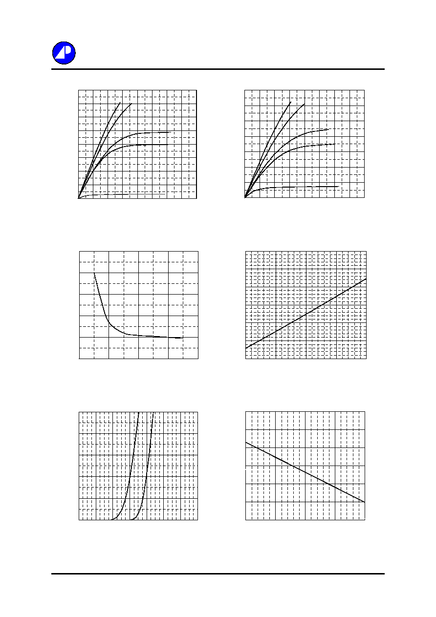
Fig 1. Typical Output Characteristics
Fig 2. Typical Output Characteristics
Fig 3. On-Resistance v.s. Gate Voltage
Fig 4. Normalized On-Resistance
v.s. Junction Temperature
Fig 5. Forward Characteristic of
Fig 6. Gate Threshold Voltage v.s.
Reverse Diode
Junction Temperature
3/4
0.6
0.8
1
1.2
1.4
1.6
1.8
-50
0
50
100
150
T
j
, Junction Temperature (
o
C )
V
GS(t
h)
(V
)
25
35
45
55
65
75
3
5
7
9
11
V
GS
, Gate-to-Source Voltage (V)
R
DS(ON)
(m
)
I
D
= 2.4 A
T
A
=25
o
C
0
5
10
15
20
25
30
35
40
0
0.5
1
1.5
2
2.5
3
3.5
4
V
DS
, Drain-to-Source Voltage (V)
I
D
, Dr
a
i
n C
u
r
r
e
nt
(A
)
10V
7.0V
5.0V
4.5V
V
G
=3.0V
T
A
=25
o
C
0
5
10
15
20
25
30
35
0
0.5
1
1.5
2
2.5
3
3.5
4
V
DS
, Drain-to-Source Voltage (V)
I
D
, Dr
a
i
n C
u
r
r
e
nt
(A
)
T
A
=150
o
C
10V
7.0V
5.0V
4.5V
V
G
=3.0V
0.6
0.8
1.0
1.2
1.4
1.6
1.8
-50
0
50
100
150
T
j
, Junction Temperature (
o
C)
N
o
rmalize
d
R
DS(ON)
I
D
=4.8A
V
G
=10V
0
1
2
3
4
5
0
0.2
0.4
0.6
0.8
1
1.2
1.4
V
SD
, Source-to-Drain Voltage (V)
I
S
(A
)
T
j
=25
o
C
T
j
=150
o
C

Fig 7. Gate Charge Characteristics
Fig 8. Typical Capacitance Characteristics
Fig 9. Maximum Safe Operating Area
Fig 10. Effective Transient Thermal Impedance
Fig 11. Switching Time Waveform
Fig 12. Gate Charge Waveform
4/4
AP2604GY
t
d(on)
t
r
t
d(off)
t
f
V
DS
V
GS
10%
90%
Q
V
G
4.5V
Q
GS
Q
GD
Q
G
Charge
10
100
1000
1
5
9
13
17
21
25
29
V
DS
, Drain-to-Source Voltage (V)
C (
p
F)
f=1.0MHz
C
iss
C
oss
C
rss
0.001
0.01
0.1
1
0.0001
0.001
0.01
0.1
1
10
100
1000
t , Pulse Width (s)
N
o
rmalize
d
The
r
mal Re
sponse
(
R
thja
)
0.01
0.05
0.1
0.2
Duty factor=0.5
Single Pulse
P
DM
Duty factor = t/T
Peak T
j
= P
DM
x R
thja
+ T
a
R
thja
= 156/W
t
T
0
4
8
12
16
0
2
4
6
8
10
12
Q
G
, Total Gate Charge (nC)
V
GS
,
G
a
te
to S
o
u
r
c
e
Voltage
(
V
)
V
DS
=15V
V
DS
=20V
V
DS
=24V
I
D
=4.8A
0.01
0.1
1
10
100
0.1
1
10
100
V
DS
, Drain-to-Source Voltage (V)
I
D
(A
)
1ms
10ms
100ms
1s
DC
T
A
=25
o
C
Single Pulse