Advanced Power
P-CHANNEL ENHANCEMENT MODE
Electronics Corp.
POWER MOSFET
Lower On-resistance
BV
DSS
-30V
Simple Drive Requirement
R
DS(ON)
14m
Fast Switching Characteristic
I
D
-50A
Description
Absolute Maximum Ratings
Symbol
Units
V
DS
V
V
GS
V
I
D
@T
C
=25
A
I
D
@T
C
=100
A
I
DM
A
P
D
@T
A
=25
W
W/
T
STG
T
J
Symbol
Value
Unit
Rthj-c
Thermal Resistance Junction-case
Max.
2.3
/W
Rthj-a
Thermal Resistance Junction-ambient
Max.
62
/W
Data and specifications subject to change without notice
200115041
AP4407S/P
Rating
-30
�25
-50
0.4
54
-55 to 150
Parameter
Drain-Source Voltage
Gate-Source Voltage
Continuous Drain Current, V
GS
@ 10V
Continuous Drain Current, V
GS
@ 10V
-32
Pulsed Drain Current
1
180
Parameter
Total Power Dissipation
Operating Junction Temperature Range
Storage Temperature Range
-55 to 150
Linear Derating Factor
Thermal Data
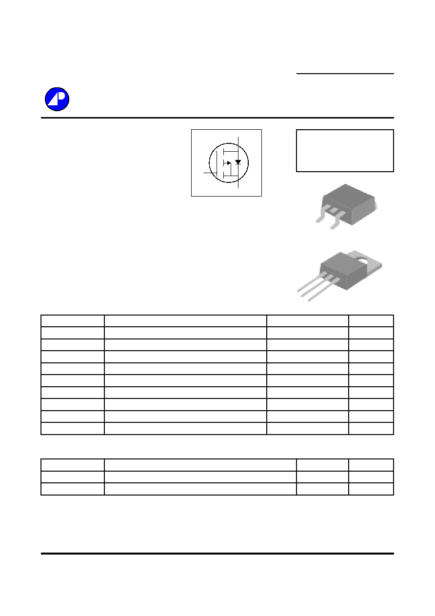
G
D
S
The Advanced Power MOSFETs from APEC provide the
designer with the best combination of fast switching,
ruggedized device design, low on-resistance and cost-effectiveness.
G D
S
TO-263(S)
G
D
S
TO-220(P)
The TO-263 package is universally preferred for all commercial-
industrial surface mount applications and suited for low voltage
applications such as DC/DC converters. The through-hole version
(AP4407P) are available for low-profile applications.
AP4407S/P
Electrical Characteristics@T
j
=25
o
C(unless otherwise specified)
Symbol
Parameter
Test Conditions
Min.
Typ. Max. Units
BV
DSS
Drain-Source Breakdown Voltage
V
GS
=0V, I
D
=-250uA
-30
-
-
V
B
V
DSS
/T
j
Breakdown Voltage Temperature Coefficient
Reference to 25
, I
D
=-1mA
-
-0.01
-
V/
R
DS(ON)
Static Drain-Source On-Resistance
2
V
GS
=-10V, I
D
=-24A
-
-
14
m
V
GS
=-4.5V, I
D
=-16A
-
-
23
m
V
GS(th)
Gate Threshold Voltage
V
DS
=V
GS
, I
D
=-250uA
-1
-
-3
V
g
fs
Forward Transconductance
V
DS
=-10V, I
D
=-24A
-
36
-
S
I
DSS
Drain-Source Leakage Current (T
j
=25
o
C)
V
DS
=-30V, V
GS
=0V
-
-
-1
uA
Drain-Source Leakage Current (T
j
=150
o
C)
V
DS
=-24V, V
GS
=0V
-
-
-25
uA
I
GSS
Gate-Source Leakage
V
GS
= �25V
-
-
nA
Q
g
Total Gate Charge
2
I
D
=-24A
-
35
60
nC
Q
gs
Gate-Source Charge
V
DS
=-24V
-
5
-
nC
Q
gd
Gate-Drain ("Miller") Charge
V
GS
=-4.5V
-
26
-
nC
t
d(on)
Turn-on Delay Time
2
V
DS
=-15V
-
11
-
ns
t
r
Rise Time
I
D
=-24A
-
64
-
ns
t
d(off)
Turn-off Delay Time
R
G
=3.3
,
V
GS
=-10V
-
63
-
ns
t
f
Fall Time
R
D
=0.63
-
100
-
ns
C
iss
Input Capacitance
V
GS
=0V
-
2120 3390
pF
C
oss
Output Capacitance
V
DS
=-25V
-
630
-
pF
C
rss
Reverse Transfer Capacitance
f=1.0MHz
-
550
-
pF
Source-Drain Diode
Symbol
Parameter
Test Conditions
Min.
Typ. Max. Units
V
SD
Forward On Voltage
2
I
S
=-24A, V
GS
=0V
-
-
-1.2
V
t
rr
Reverse Recovery Time
2
I
S
=-24A, V
GS
=0V,
-
39
-
ns
Q
rr
Reverse Recovery Charge
dI/dt=-100A/�s
-
38
-
nC
Notes:
1.Pulse width limited by safe operating area.
2.Pulse width <300us , duty cycle <2%.
�
100
AP4407S/P
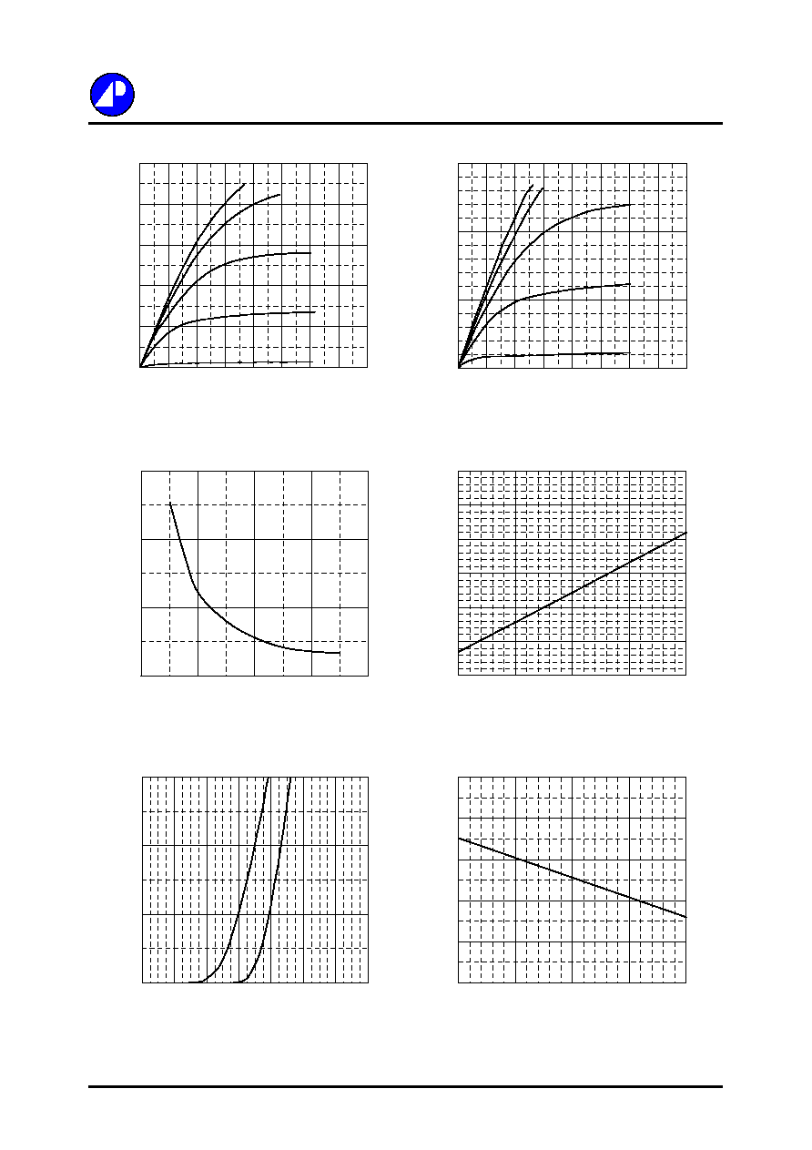
Fig 1. Typical Output Characteristics
Fig 2. Typical Output Characteristics
Fig 3. On-Resistance v.s. Gate Voltage
Fig 4. Normalized On-Resistance
v.s. Junction Temperature
Fig 5. Forward Characteristic of
Fig 6. Gate Threshold Voltage v.s.
Reverse Diode
Junction Temperature
0
10
20
30
0
0.2
0.4
0.6
0.8
1
1.2
1.4
-V
SD
, Source-to-Drain Voltage (V)
-I
S
(A
)
T
j
=25
o
C
T
j
=150
o
C
0
50
100
150
200
250
0
1
2
3
4
5
6
7
8
-V
DS
, Drain-to-Source Voltage (V)
-I
D
, Drain
Cu
rre
n
t
(A)
T
C
=25
o
C
-10V
-8.0V
-6.0V
-4.5V
V
G
=-3.0V
10
15
20
25
3
5
7
9
11
-V
GS
, Gate-to-Source Voltage (V)
R
DS(
ON)
(m
)
I
D
= -16 A
T
C
=25
0
50
100
150
0
1
2
3
4
5
6
7
8
-V
DS
, Drain-to-Source Voltage (V)
-I
D
, Drain
Cu
rre
n
t
(A)
-10V
-8.0V
-6.0V
-4.5V
V
G
=-3.0V
T
C
=150
o
C
0.6
0.8
1.0
1.2
1.4
1.6
1.8
-50
0
50
100
150
T
j
, Junction Temperature (
o
C)
N
o
rmalize
d
R
DS(
ON)
I
D
=-24A
V
G
=-10V
0.5
1.0
1.5
2.0
2.5
3.0
-50
0
50
100
150
T
j
, Junction Temperature (
o
C)
-V
GS(
t
h)
(V
)
AP4407S/P
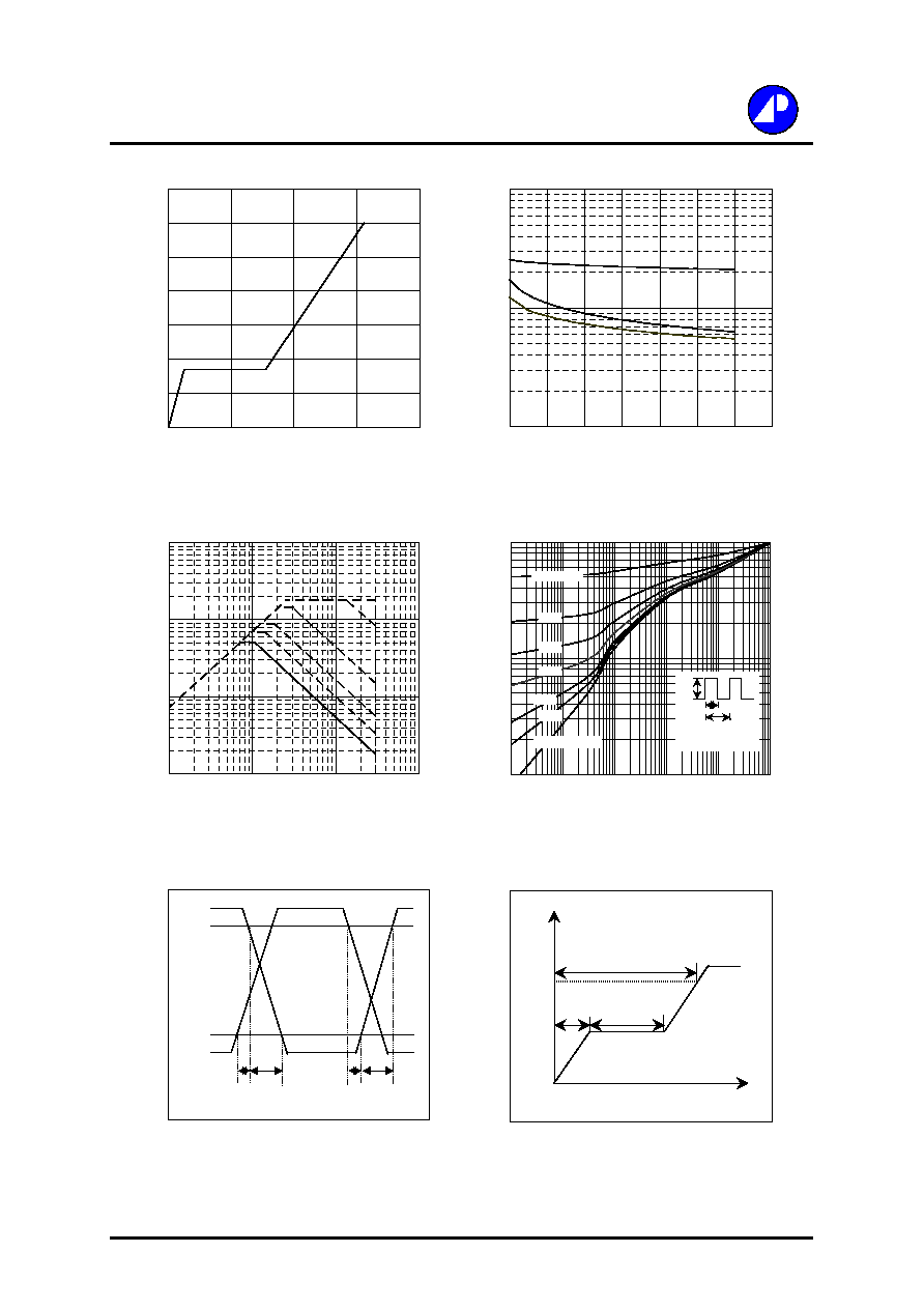
Fig 7. Gate Charge Characteristics
Fig 8. Typical Capacitance Characteristics
Fig 9. Maximum Safe Operating Area
Fig 10. Effective Transient Thermal Impedance
Fig 11. Switching Time Waveform
Fig 12. Gate Charge Waveform
t
d(on)
t
r
t
d(off)
t
f
V
DS
V
GS
10%
90%
Q
V
G
-4.5V
Q
GS
Q
GD
Q
G
Charge
100
1000
10000
1
5
9
13
17
21
25
29
-V
DS
, Drain-to-Source Voltage (V)
C (p
F)
f=1.0MHz
C
iss
C
oss
C
rss
0
2
4
6
8
10
12
14
0
20
40
60
80
Q
G
, Total Gate Charge (nC)
-V
GS
, Gate
to S
o
u
r
c
e
V
oltage
(
V
)
I
D
= - 24 A
V
DS
= -24V
1
10
100
1000
0.1
1
10
100
-V
DS
, Drain-to-Source Voltage (V)
-I
D
(A)
T
C
=25
o
C
Single Pulse
100us
1ms
10ms
100ms
DC
0.01
0.1
1
0.00001
0.0001
0.001
0.01
0.1
1
t , Pulse Width (s)
Norm
alize
d
Th
e
r
m
al R
e
spon
se
(
R
th
jc
)
P
DM
Duty factor = t/T
Peak T
j
= P
DM
x R
thjc
+ T
C
t
T
0.02
0.01
0.05
0.1
0.2
Duty factor=0.5
Single Pulse