
Advanced Power
N AND P-CHANNEL ENHANCEMENT
Electronics Corp.
MODE POWER MOSFET
Simple Drive Requirement
N-CH BV
DSS
30V
Low On-resistance
R
DS(ON)
28m
Fast Switching
I
D
7A
P-CH BV
DSS
-30V
R
DS(ON)
5
0
m
Description
I
D
-5.3A
Absolute Maximum Ratings
Symbol
Parameter
Rating
Units
N-channel P-channel
V
DS
Drain-Source Voltage
-30
V
V
GS
Gate-Source Voltage
�20
V
I
D
@T
A
=25
Continuous Drain Current
3
-5.3
A
I
D
@T
A
=70
Continuous Drain Current
3
-4.7
A
I
DM
Pulsed Drain Current
1
-20
A
P
D
@T
A
=25
Total Power Dissipation
W
Linear Derating Factor
W/
T
STG
Storage Temperature Range
T
J
Operating Junction Temperature Range
Symbol
Value
Unit
Rthj-amb
Thermal Resistance Junction-ambient
3
Max.
62.5
/W
Data and specifications subject to change without notice
-55 to 150
0.016
-55 to 150
5.8
20
2
Parameter
201225022
AP4501M
Thermal Data
30
�20
7
The Advanced Power MOSFETs from APEC provide the
designer with the best combination of fast switching,
ruggedized device design, low on-resistance and cost-
effectiveness.
The SO-8 package is universally preferred for all commercial-
industrial surface mount applications and suited for low voltage
applications such as DC/DC converters.
G2
D2
S2
G1
D1
S1
S1
G1
S2
G2
D1
D1
D2
D2
SO-8
N-CH Electrical Characteristics@T
j
=25
o
C(unless otherwise specified)
Symbol
Parameter
Test Conditions
Min. Typ. Max. Units
BV
DSS
Drain-Source Breakdown Voltage
V
GS
=0V, I
D
=250uA
30
-
-
V
B
V
DSS
/T
j
Breakdown Voltage Temperature Coefficient
Reference to 25
, I
D
=1mA
-
0.02
-
V/
R
DS(ON)
Static Drain-Source On-Resistance
2
V
GS
=10V, I
D
=7A
-
-
28
m
V
GS
=4.5V, I
D
=5A
-
-
42
m
V
GS(th)
Gate Threshold Voltage
V
DS
=V
GS
, I
D
=250uA
1
-
3
V
g
fs
Forward Transconductance
V
DS
=10V, I
D
=7A
-
13
-
S
I
DSS
Drain-Source Leakage Current (T
j
=25
o
C)
V
DS
=30V, V
GS
=0V
-
-
1
uA
Drain-Source Leakage Current (T
j
=70
o
C)
V
DS
=24V, V
GS
=0V
-
-
25
uA
I
GSS
Gate-Source Leakage
V
GS
=�20V
-
-
nA
Q
g
Total Gate Charge
2
I
D
=7A
-
8.4
-
nC
Q
gs
Gate-Source Charge
V
DS
=24V
-
2.1
-
nC
Q
gd
Gate-Drain ("Miller") Charge
V
GS
=4.5V
-
4.7
-
nC
t
d(on)
Turn-on Delay Time
2
V
DS
=15V
-
6
-
ns
t
r
Rise Time
I
D
=1A
-
5.2
-
ns
t
d(off)
Turn-off Delay Time
R
G
=3.3
,
V
GS
=10V
-
18.8
-
ns
t
f
Fall Time
R
D
=15
-
4.4
-
ns
C
iss
Input Capacitance
V
GS
=0V
-
645
-
pF
C
oss
Output Capacitance
V
DS
=25V
-
150
-
pF
C
rss
Reverse Transfer Capacitance
f=1.0MHz
-
95
-
pF
Source-Drain Diode
Symbol
Parameter
Test Conditions
Min. Typ. Max. Units
I
S
Continuous Source Current ( Body Diode )
V
D
=V
G
=0V , V
S
=1.2V
-
-
1.67
A
V
SD
Forward On Voltage
2
T
j
=25
, I
S
=7A, V
GS
=0V
-
-
1.2
V
AP4501M
�
100

AP4501M
P-CH Electrical Characteristics@T
j
=25
o
C(unless otherwise specified)
Symbol
Parameter
Test Conditions
Min. Typ. Max. Units
BV
DSS
Drain-Source Breakdown Voltage
V
GS
=0V, I
D
=-250uA
-30
-
-
V
B
V
DSS
/T
j
Breakdown Voltage Temperature Coefficient
Reference to 25
, I
D
=-1mA
-
-0.028
-
V/
R
DS(ON)
Static Drain-Source On-Resistance
2
V
GS
=-10V, I
D
=-5.3A
-
-
50
m
V
GS
=-4.5V, I
D
=-4.2A
-
-
90
m
V
GS(th)
Gate Threshold Voltage
V
DS
=V
GS
, I
D
=-250uA
-1
-
-3
V
g
fs
Forward Transconductance
V
DS
=-10V, I
D
=-5.3A
-
8.5
-
S
I
DSS
Drain-Source Leakage Current (T
j
=25
o
C)
V
DS
=-30V, V
GS
=0V
-
-
-1
uA
Drain-Source Leakage Current (T
j
=70
o
C)
V
DS
=-24V, V
GS
=0V
-
-
-25
uA
I
GSS
Gate-Source Leakage
V
GS
=
-
-
nA
Q
g
Total Gate Charge
2
I
D
=-5.3A
-
20
-
nC
Q
gs
Gate-Source Charge
V
DS
=-15V
-
3.5
-
nC
Q
gd
Gate-Drain ("Miller") Charge
V
GS
=-10V
-
2
-
nC
t
d(on)
Turn-on Delay Time
2
V
DS
=-15V
-
12
-
ns
t
r
Rise Time
I
D
=-1A
-
20
-
ns
t
d(off)
Turn-off Delay Time
R
G
=6
,
V
GS
=-10V
-
45
-
ns
t
f
Fall Time
R
D
=15
-
27
-
ns
C
iss
Input Capacitance
V
GS
=0V
-
790
-
pF
C
oss
Output Capacitance
V
DS
=-15V
-
440
-
pF
C
rss
Reverse Transfer Capacitance
f=1.0MHz
-
120
-
pF
Source-Drain Diode
Symbol
Parameter
Test Conditions
Min. Typ. Max. Units
I
S
Continuous Source Current ( Body Diode )
V
D
=V
G
=0V , V
S
=-1.2V
-
-
-1.67 A
V
SD
Forward On Voltage
2
T
j
=25
, I
S
=-2.6A, V
GS
=0V
-
-
-1.2
V
Notes:
1.Pulse width limited by Max. junction temperature.
2.Pulse width <300us , duty cycle <2%.
3.Surface mounted on 1 in
2
copper pad of
FR4 board ; 135
/W when mounted on Min. copper pad.
�
20V
�
100
�
20V
�
100
�
20V
N-Channel
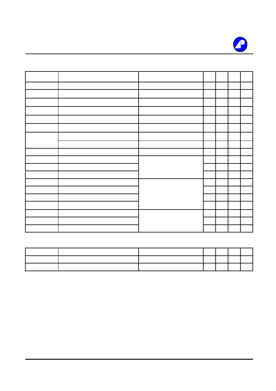
Fig 1. Typical Output Characteristics
Fig 2. Typical Output Characteristics
Fig 3. On-Resistance v.s. Gate Voltage
Fig 4. Normalized On-Resistance
v.s. Junction Temperature
AP4501M
0
12
24
36
0
2
3
5
6
V
DS
, Drain-to-Source Voltage (V)
I
D
,
Dr
a
i
n C
u
r
r
e
nt
(A
)
T
C
=25
o
C
10V
8.0V
6.0V
5.0V
V
GS
=4.5V
0.2
0.8
1.4
2
-50
0
50
100
150
T
j
, Junction Temperature (
o
C)
N
o
r
m
aliz
e
d
R
DS
(
ON)
I
D
=7.0A
V
GS
= 10V
10
30
50
70
90
2
6
10
14
V
GS
(V)
R
DS
(
ON)
(m
)
I
D
=7.0A
T
C
=25
0
12
24
36
0
2
3
5
6
V
DS
, Drain-to-Source Voltage (V)
I
D
,
Dr
a
i
n C
u
r
r
e
nt
(A
)
T
C
=150
o
C
10V
8.0V
6.0V
5.0V
V
GS
=4.5V
AP4501M
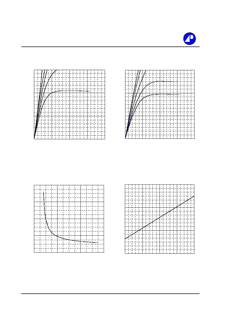
N-Channel
Fig 5. Maximum Drain Current v.s.
Fig 6. Typical Power Dissipation
Case Temperature
Fig 7. Maximum Safe Operating Area
Fig 8. Effective Transient Thermal Impedance
0
2
4
6
8
25
50
75
100
125
150
T
c
, Case Temperature (
o
C)
I
D
,
Dr
a
i
n C
u
r
r
e
nt
(A
)
0
0.6
1.2
1.8
2.4
0
50
100
150
T
c
,Case Temperature (
o
C)
P
D
(W
)
0.001
0.01
0.1
1
0.0001
0.001
0.01
0.1
1
10
100
1000
t , Pulse Width (s)
N
o
r
m
aliz
ed T
h
er
m
a
l Res
pon
s
e
(
R
th
ja
)
P
DM
Duty Factor = t/T
Peak T
j
= P
DM
x R
thja
+ T
a
R
thja
=135
o
C/W
t
T
0.02
0.01
0.05
0.1
0.2
Duty Factor = 0.5
Single Pulse
0.01
0.1
1
10
100
0.1
1
10
100
V
DS
(V)
I
D
(A
)
T
C
=25
o
C
Single Pulse
1ms
10ms
100ms
1s
10s
DC