
Advanced Power
N AND P-CHANNEL ENHANCEMENT
Electronics Corp.
MODE POWER MOSFET
Simple Drive Requirement
N-CH BV
DSS
35V
Good Thermal Performance
R
DS(ON)
30m
Fast Switching Performance
I
D
15A
P-CH BV
DSS
-35V
R
DS(ON)
48m
Description
I
D
-12A
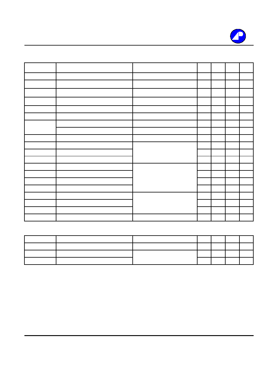
Absolute Maximum Ratings
Symbol
Parameter
Rating
Units
N-channel P-channel
V
DS
Drain-Source Voltage
35
-35
V
V
GS
Gate-Source Voltage
�20
�20
V
I
D
@T
C
=25
Continuous Drain Current
3
15
-12
A
I
D
@T
C
=100
Continuous Drain Current
3
9
-7
A
I
DM
Pulsed Drain Current
1
50
-50
A
P
D
@T
C
=25
Total Power Dissipation
10.4
W
Linear Derating Factor
0.083
W/
T
STG
Storage Temperature Range
-55 to 150
T
J
Operating Junction Temperature Range
-55 to 150
Symbol
Value
Units
Rthj-c
Thermal Resistance Junction-case
3
Max.
12
/W
Rthj-a
Thermal Resistance Junction-ambient
3
Max.
110
/W
Data and specifications subject to change without notice
Parameter
200222053
Thermal Data
AP4511GH
Pb Free Plating Product
G2
D2
S2
G1
D1
S1
The Advanced Power MOSFETs from APEC provide the
designer with the best combination of fast switching,
ruggedized device design, low on-resistance and cost-
effectiveness.
S1
TO-252-4L
G1
S2
G2
D1/D2
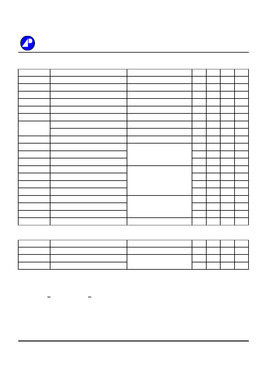
N-CH Electrical Characteristics@T
j
=25
o
C(unless otherwise specified)
Symbol
Parameter
Test Conditions
Min.
Typ. Max. Units
BV
DSS
Drain-Source Breakdown Voltage
V
GS
=0V, I
D
=250uA
35
-
-
V
B
V
DSS
/T
j
Breakdown Voltage Temperature Coefficient
Reference to 25
, I
D
=1mA
-
0.03
-
V/
R
DS(ON)
Static Drain-Source On-Resistance
2
V
GS
=10V, I
D
=8A
-
-
30
m
V
GS
=4.5V, I
D
=6A
-
-
40
m
V
GS(th)
Gate Threshold Voltage
V
DS
=V
GS
, I
D
=250uA
1
-
3
V
g
fs
Forward Transconductance
V
DS
=10V, I
D
=8A
-
13
-
S
I
DSS
Drain-Source Leakage Current (T
j
=25
o
C)
V
DS
=35V, V
GS
=0V
-
-
1
uA
Drain-Source Leakage Current (T
j
=150
o
C)
V
DS
=28V, V
GS
=0V
-
-
25
uA
I
GSS
Gate-Source Leakage
V
GS
=�20V
-
-
nA
Q
g
Total Gate Charge
2
I
D
=8A
-
11
18
nC
Q
gs
Gate-Source Charge
V
DS
=28V
-
3
-
nC
Q
gd
Gate-Drain ("Miller") Charge
V
GS
=4.5V
-
6
-
nC
t
d(on)
Turn-on Delay Time
2
V
DS
=18V
-
12
-
ns
t
r
Rise Time
I
D
=1A
-
7
-
ns
t
d(off)
Turn-off Delay Time
R
G
=3.3
,
V
GS
=10V
-
22
-
ns
t
f
Fall Time
R
D
=18
-
6
-
ns
C
iss
Input Capacitance
V
GS
=0V
-
830
1330
pF
C
oss
Output Capacitance
V
DS
=25V
-
150
-
pF
C
rss
Reverse Transfer Capacitance
f=1.0MHz
-
110
-
pF
R
g
Gate Resistance
f=1.0MHz
-
1.1
1.7
Source-Drain Diode
Symbol
Parameter
Test Conditions
Min.
Typ. Max. Units
V
SD
Forward On Voltage
2
I
S
=8A, V
GS
=0V
-
-
1.2
V
t
rr
Reverse Recovery Time
2
I
S
=8A, V
GS
=0V
-
18
-
ns
Q
rr
Reverse Recovery Charge
dI/dt=100A/�s
-
12
-
nC
AP4511GH
�
100
AP4511GH
P-CH Electrical Characteristics@T
j
=25
o
C(unless otherwise specified)
Symbol
Parameter
Test Conditions
Min.
Typ. Max. Units
BV
DSS
Drain-Source Breakdown Voltage
V
GS
=0V, I
D
=-250uA
-35
-
-
V
B
V
DSS
/T
j
Breakdown Voltage Temperature Coefficient
Reference to 25
,I
D
=-1mA
-
-0.03
-
V/
R
DS(ON)
Static Drain-Source On-Resistance
2
V
GS
=-10V, I
D
=-6A
-
-
48
m
V
GS
=-4.5V, I
D
=-4A
-
-
70
m
V
GS(th)
Gate Threshold Voltage
V
DS
=V
GS
, I
D
=-250uA
-1
-
-3
V
g
fs
Forward Transconductance
V
DS
=-10V, I
D
=-6A
-
10
-
S
I
DSS
Drain-Source Leakage Current (T
j
=25
o
C)
V
DS
=-35V, V
GS
=0V
-
-
-1
uA
Drain-Source Leakage Current (T
j
=150
o
C)
V
DS
=-28V, V
GS
=0V
-
-
-25
uA
I
GSS
Gate-Source Leakage
V
GS
=�20V
-
-
nA
Q
g
Total Gate Charge
2
I
D
=-6A
-
10
19
nC
Q
gs
Gate-Source Charge
V
DS
=-28V
-
2
-
nC
Q
gd
Gate-Drain ("Miller") Charge
V
GS
=-4.5V
-
6
-
nC
t
d(on)
Turn-on Delay Time
2
V
DS
=-18V
-
10
-
ns
t
r
Rise Time
I
D
=-1A
-
6
-
ns
t
d(off)
Turn-off Delay Time
R
G
=3.3
,V
GS
=-10V
-
26
-
ns
t
f
Fall Time
R
D
=18
-
7
-
ns
C
iss
Input Capacitance
V
GS
=0V
-
690
1100
pF
C
oss
Output Capacitance
V
DS
=-25V
-
165
-
pF
C
rss
Reverse Transfer Capacitance
f=1.0MHz
-
130
-
pF
R
g
Gate Resistance
f=1.0MHz
-
5
7.5
Source-Drain Diode
Symbol
Parameter
Test Conditions
Min.
Typ. Max. Units
V
SD
Forward On Voltage
2
I
S
=-6A, V
GS
=0V
-
-
-1.2
V
t
rr
Reverse Recovery Time
2
I
S
=-6A, V
GS
=0V
-
20
-
ns
Q
rr
Reverse Recovery Charge
dI/dt=-100A/�s
-
12
-
nC
Notes:
1.Pulse width limited by Max. junction temperature.
2.Pulse width <300us , duty cycle <2%.
3.N-CH , P-CH are same .
�
100

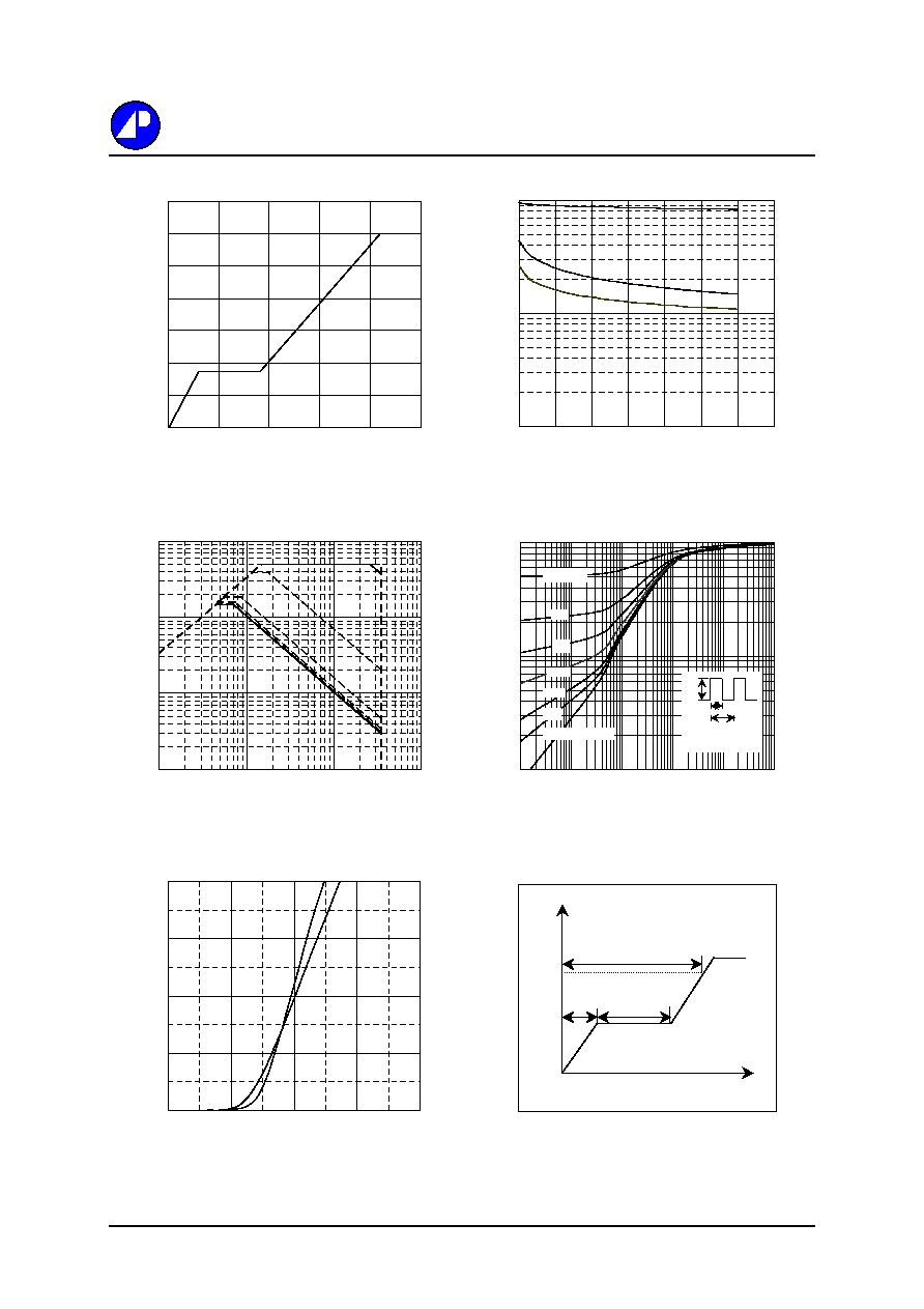
N-Channel
Fig 1. Typical Output Characteristics
Fig 2. Typical Output Characteristics
Fig 3. On-Resistance v.s. Gate Voltage
Fig 4. Normalized On-Resistance
v.s. Junction Temperature
Fig 5. Forward Characteristic of
Fig 6. Gate Threshold Voltage v.s.
Reverse Diode
Junction Temperature
AP4511GH
0
10
20
30
40
50
0
1
2
3
4
5
V
DS
, Drain-to-Source Voltage (V)
I
D
,
Dr
a
i
n C
u
r
r
e
nt
(A
)
T
C
= 25
o
C
10V
7.0V
5.0V
4.5V
V
G
=3.0V
0
2
4
6
0
0.2
0.4
0.6
0.8
1
1.2
V
SD
, Source-to-Drain Voltage (V)
I
S
(A
)
T
j
=25
o
C
T
j
=150
o
C
0
10
20
30
40
50
0
1
2
3
4
5
V
DS
, Drain-to-Source Voltage (V)
I
D
,
Dr
a
i
n C
u
r
r
e
nt
(A
)
T
C
= 150
o
C
10V
7.0V
5.0V
4.5V
V
G
=3.0V
20
25
30
35
40
45
2
4
6
8
10
V
GS
, Gate-to-Source Voltage (V)
R
DS
(
ON)
(m
)
I
D
= 6 A
T
C
=25
o
C
0.6
0.8
1.0
1.2
1.4
1.6
-50
0
50
100
150
T
j
, Junction Temperature (
o
C)
N
o
r
m
aliz
ed R
DS
(
ON)
I
D
= 8 A
V
G
=10V
0.5
0.8
1.1
1.4
-50
0
50
100
150
T
j
, Junction Temperature (
o
C)
N
o
r
m
aliz
ed V
GS
(
t
h
)
(V
)
AP4511GH
N-Channel
Fig 7. Gate Charge Characteristics
Fig 8. Typical Capacitance Characteristics
Fig 9. Maximum Safe Operating Area
Fig 10. Effective Transient Thermal Impedance
Fig 11. Transfer Characteristics
Fig 12. Gate Charge Waveform
Q
V
G
4.5V
Q
GS
Q
GD
Q
G
Charge
10
100
1000
1
5
9
13
17
21
25
29
V
DS
, Drain-to-Source Voltage (V)
C (
p
F)
f=1.0MHz
C
iss
C
oss
C
rss
0
10
20
30
40
0
2
4
6
8
V
GS
, Gate-to-Source Voltage (V)
I
D
,
Dr
a
i
n C
u
r
r
e
nt
(A
)
T
j
=150
o
C
T
j
=25
o
C
V
DS
=5V
0.1
1
10
100
0.1
1
10
100
V
DS
, Drain-to-Source Voltage (V)
I
D
(A
)
100us
1ms
10ms
100ms
DC
T
C
=25
o
C
Single Pulse
0
2
4
6
8
10
12
14
0
5
10
15
20
25
Q
G
, Total Gate Charge (nC)
V
GS
, G
a
te to S
o
u
r
ce Voltage (
V
)
I
D
= 8 A
V
DS
= 28V
0.01
0.1
1
0.00001
0.0001
0.001
0.01
0.1
1
t , Pulse Width (s)
N
o
r
m
aliz
ed T
h
er
m
a
l Res
pon
s
e
(
R
th
jc
)
P
DM
Duty factor = t/T
Peak T
j
= P
DM
x R
thjc
+ T
C
t
T
0.02
0.01
0.05
0.1
0.2
Duty factor=0.5
Single Pulse