 | –≠–ª–µ–∫—Ç—Ä–æ–Ω–Ω—ã–π –∫–æ–º–ø–æ–Ω–µ–Ω—Ç: AAT1011A | –°–∫–∞—á–∞—Ç—å:  PDF PDF  ZIP ZIP |

Advanced Analog Technology, Inc.
≠
≠
Advanced Analog Technology, Inc
. V 1.0
AAT1011A
3-CHANNEL PC POWER SUPPLY SUPERVISOR
FOR 3.3V, 5V AND 12V
Features
3-Channel PC Power Supply Supervisor with
Minimized External Components
Over Voltage Protection for 3.3V / 5V / 12V
Output
Under Voltage Protection for 3.3V / 5V
Output with 75 ms Enable Delay
Fault Protection Output with Open Drain
Output
Open Drain Power Good Output
300 ms Power Good Delay
2.3 ms
ONCTL to FPO Turn Off Delay
49 ms ONCTL Signal De-bounce
73
µs De-bounce
Latch Function Controlled by ONCTL and
Protection Input
8KV Highly Qualified ESD Protection
Pin Configuration
General Description
The AAT1011 is a 3-channel power supply
supervisor with 8KV ESD protection. It provides
Over Voltage Protection (OVP), Under Voltage
Protection (UVP), and Power Good Indicator to
monitor and control the output of the switching
power supply system.
Remote function from external signal, i.e., On/Off
Control ( ONCTL ), is also implemented.
Over voltage fault protection and under voltage
fault protection can be directly triggered without
external voltage divider.
With a minimum number of external components,
the AAT1011 offers a simple and cost effective
solution. Meanwhile, it can greatly reduce the
PCB board space for power supply system.
*Spec is subject to change without notice in this document.
1
2
3
4
5
6
7
8
PGI
GND
FPO
ONCTL
PGO
Vcc
V5
V33
TOP VIEW
(PDIP-8 PACKAGE)

Advanced Analog Technology, Inc.
≠
≠
Advanced Analog Technology, Inc
. V 1.0
AAT1011A
FPO (Fault Protection Output)
NORMAL="LOW", FAULT="HIGH"
FPO indicates the fault condition of either Over
Voltage or Under Voltage. When a fault state
occurs, the FPO latched high and combined with a
low PGO output.
PGO (Power Good Output)
NORMAL="HIGH", FAULT="LOW".
The Power Good signal will be issued with 300
ms delay after 3.3V, 5V, 12V and PGI are ready.
Power Good Output should be low before the
output voltage is out of regulation at turn-off.
OVP and UVP
OVP monitors 3.3V, 5V, and 12V (via Vcc pin)
UVP monitors 3.3V and 5V. OVP and UVP
levels are determined by internal voltage dividers.
The typical values are 3.9V, 6.1V, 13.8V for OVP
and 2.83V, 4.3V for UVP, respectively.
ONCTL (On/Off Control)
On/Off Control is used to reset the latched state of
FPO and to externally control the switching
power supply system with a 49 ms de-bounce time.
AAT1011 offers 2.3 ms delay time after de-bounce
to trigger FPO when ONCTL switches from
low to high
.
Advanced Analog Technology, Inc.
≠
≠
Advanced Analog Technology, Inc
. V 1.0
AAT1011A
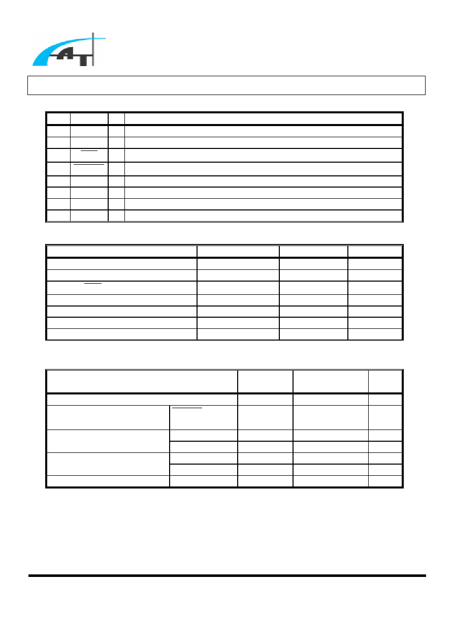
Pin Description
Pin
# Name I/O
Description
1
PGI
I Power Good Input signal
2 GND
Ground
3
FPO
O Inverted Fault Protection Output, open drain output stage
4
ONCTL I ON/OFF control input
5
V33
I Over and Under Voltage Protection for 3.3V
6
V5
I Over and Under Voltage Protection for 5V
7 V
CC
I Supply voltage and 12V over voltage protection input
8
PGO
O Power Good Output signal, open drain output stage
Absolute Maximum Ratings
CHARACTERISTICS SYMBOL
VALUE
UNIT
Supply voltage
V
CC
16
V
ESD voltage
V
ESD
8
KV
FPO output voltage
V
FPO
16
V
PGO output voltage
V
PGO
8
V
Supply Current
I
CC
1
mA
Operating free-air temperature range
T
op
-25 ~ 85
o
C
Storage temperature range
T
stg
-65 ~ 125
o
C
Recommended Operating Conditions
Test
Condition
Min Typ Max Unit
Supply voltage, V
CC
4
15
V
Input voltage, V
I
ONCTL , V5,
V33, PGI
7
V
V
FPO
15
V
Output voltage
V
PGO
7
V
I
FPO
30
mA
Output sink current, I
O
(sink)
I
PGO
10
mA
Supply voltage rising time, t
r
See Note 1
1
ms
Note 1: V
CC
slew rate must be less than 14 V/ms.
Advanced Analog Technology, Inc.
≠
≠
Advanced Analog Technology, Inc
. V 1.0
AAT1011A
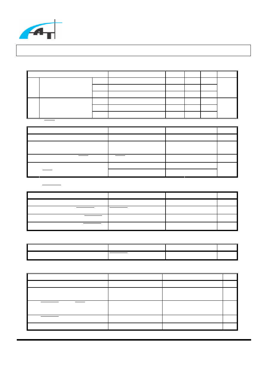
Electrical Characteristics, V
CC
= 5 V (Unless Otherwise Specified)
Over Voltage Protection and Under Voltage Protection
Parameter Test
Condition
Min
Typ
Max
Unit
V33
3.7 3.9 4.1
V5
5.7 6.1 6.5
Over voltage threshold
V
CC
13.3 13.8 14.3
V
V33
2.71 2.83 2.95
V 5
4.1
4.3
4.47
Under-voltage
threshold
V
CC
3.8
V
PGO and
FPO
Parameter Test
Condition
Min
Typ
Max
Unit
I
LKG
Leakage current (PGO)
PGO = 5 V
5
µA
V
OL
Low level output voltage
(PGO)
I
sink
= 10 mA
0.4
V
I
LKG
Leakage current ( FPO ) V( FPO ) = 5 V
5
µA
I
sink
= 10 mA
0.3
V
OL
Low level output voltage
( FPO )
I
sink
= 30 mA
0.7
V
PGI and ONCTL
Parameter Test
Condition
Min
Typ
Max
Unit
Input threshold voltage (PGI)
1.141 1.192 1.242
V
Input pull-up current ( ONCTL )
ONCTL = 0 V
150 µA
High-level input voltage ( ONCTL ) 2.0
V
Low-level input voltage ( ONCTL )
0.8
V
Operating Current
Parameter Test
Condition
Min
Typ
Max
Unit
I
CC
Supply
current
ONCTL = 5 V
1
mA
Switching Characteristics, V
CC
= 5V, T
op
= Full Range
Parameter Test
Condition
Min
Typ
Max
Unit
t
d1
PGO delay time
200
300
450
ms
t
d2
Under Voltage Protection
delay time
49
75
114
ms
t
d3
ONCTL off to FPO delay
time
tb1+1.1 tb1+2.3 tb1+4.4 ms
t
b1
ONCTL de-bounce time
32.7
49
73.5
ms
t
b2
Noise de-bounce time
47
73
110
µs

Advanced Analog Technology, Inc.
≠
≠
Advanced Analog Technology, Inc
. V 1.0
AAT1011A
Function Block Diagram
Vref
Power on Reset
Reset
V
INT
V
INT
=3.58 V
UVLO
PGI
Vref
300 ms
Delay
CLR
POD
Vref
73 µs
Debounce
R
73 µs
Debounce
R
75 ms
Delay
R
Bandgap
Reference
V
BG
=1.28
ONCTL
150 uA
Vcc
49 ms
Debounce
Reset
POD
Oscillator
Reset
POD
POD2
2.3 ms
Delay
*
CLR
Vcc
GND
V33
V5
UV5
UV33
UV5
OV5
UV33
OV33
OV12
Vref
73 µs
Debounce
R
Vref
Vref
POD
POD2
R
Reset
R
S
OV12
OV5
OV33
Q
S
R
Q
Q
FPO
Level
Shift
PGO
Level
Shift