≠
≠
≠
≠
Page 1 of 18 V4.0
AAT1102
Product information presented is current as of publication date. Details are subject to change without notice
ADVANCED PWM DC-DC CONVERTER WITH
INTERNAL SWITCH AND SOFT-START
FEATURES
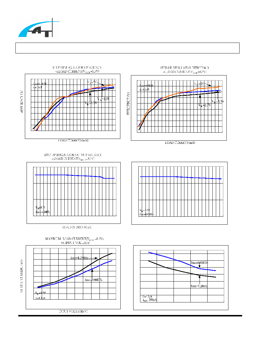
1.6A, 0.23 , Internal Switch
High Efficiency: 90%
Adjustable Output:
DD
V to 12.5V
Adjustable Frequency: 640kHz or 1.3MHz
Wide Input Range: +2.6V to +5.5V
Low Shutdown Current:
A
1
.
0
Programmable Soft-Start
Small 8-Pin MSOP Package
PIN CONFIGURATION
GENERAL DESCRIPTION
The AAT1102 is a step-up DC-DC converter with
a 1.6A,
23
.
0
internal switch. Equipped with an
external compensation pin, this device offers user
flexibility in determining loop dynamic and
adjusting operating frequency. AAT1102 also
allows the use of small, low equivalent resistance
(ESR) ceramic output capacitor, and it's capable
of converting a standard input of 3.3V to multiple
outputs of 8V,
V
8 , and 23V. Furthermore,
filtering and loop performance are facilitated and
enhanced by a high switching frequency of either
640 kHz or1.3MHz.
The AAT1102's versatility comes with a
power-smart design. A soft-start programmed
with an external capacitor that sets the input
current ramp rate, reduces the current
consumption to
A
1
.
0
in shutdown mode. When
operating, a mere 2.6V input yields an impressive
output voltage as high as 12.5V.
High switching frequency and economical design
allow AAT1102 to be less than 1.1mm high. Its
compact 8-pin MSOP package and superior
performance make it an ideal part for biasing TFT
displays.
AAT1102
8
7
6
5
1
2
3
4
SS
FREQ
V
DD
SW
EO
IN
GND
SHDN
8-Pin MSOP
TOP VIEW
≠
≠
≠
≠
Page 2 of 18 V4.0
AAT1102
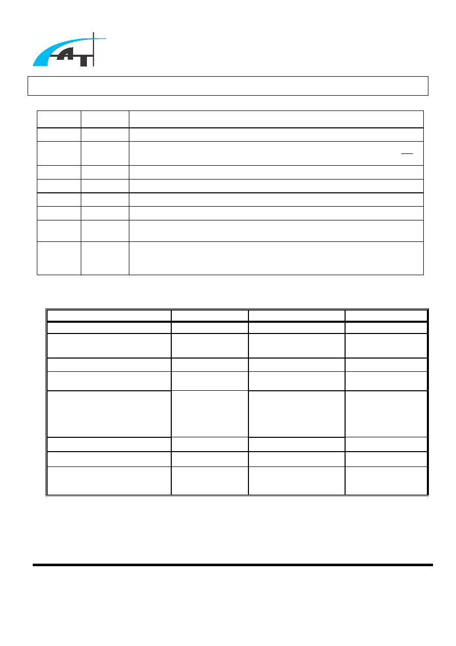
PIN DESCRIPTIONS
PIN
NAME
FUNCTION
1
EO
Compensation Pin for Error Amplifier
2
IN
Feedback Pin with a Typical Reference Voltage of 1.24V,
OUT
V
= IN(1+
R2
R1
)
3
SHDN Shutdown Control Pin. The Device Will Turn Off When SHDN is Low
4
GND
Ground
5
SW
Switch Pin
6
DD
V
Power Supply Pin
7
FREQ
Frequency Select Pin. Switch Oscillator Frequency to 640kHz When FREQ is
Low, and 1.3MHz When FREQ is High
8
SS
Soft-Start Control Pin. No Soft-Start When the Pin is Left Open
ABSOLUTE MAXIMUM RATINGS
PARAMETER
SYMBOL
VALUE
UNIT
SW to GND
3
.
0 to +18
V
IN, SHDN,
DD
V
, FREQ to
GND
3
.
0 to +6
V
SS, EO to GND
3
.
0 V to (
DD
V
+ 0.3V)
V
RMS SW Pin Current
SW
I
1.2
A
Continuous Power Dissipation
(
C
T
=
70 )
8-Pin MSOP (De-Rate
mW
1
.
4
/ above +70 )
d
P
330
mW
Operation Temperature Range
C
T
20 to +85
Storage Temperature Range
storage
T
45 to +125
Lead Temperature
(Soldering for 10 seconds)
L
T
+300
Note:
1. Absolute Maximum Ratings are threshold limit values that must not be exceeded.
2. Operation above these absolute maximum ratings may cause degradation or permanent damage to the device.
3. These are stress ratings only and do not necessarily imply functional operation below these limits.
≠
≠
≠
≠
Page 3 of 18 V4.0
AAT1102
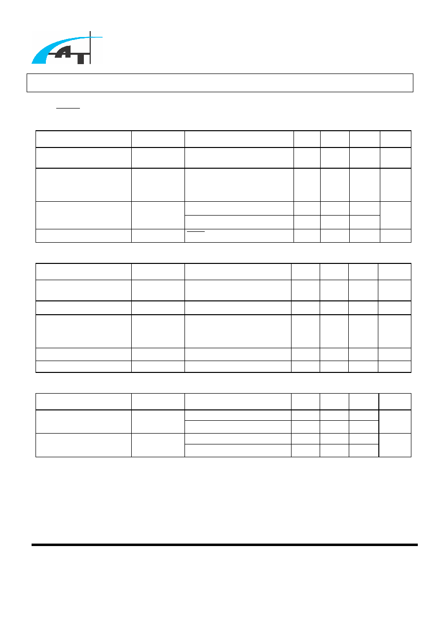
ELECTRICAL CHARACTERISTICS
DD
V
3V
SHDN
, FREQ = GND
,
unless otherwise specified. Typical values are at
C
T
C
25
)
PARAMETER
SYMBOL
CONDITIONS
MIN TYP MAX UNITS
Input Supply Voltage
Range
DD
V
2.6
5.5
V
DD
V
Under Voltage
Lockout
UVLO
When
DD
V
is rising, typical
hysteresis is 40mV; SW
remains off below this level
2.25 2.38
2.52
V
IN
V = 1.3V, not switching
0.21
0.35
Quiescent Current
DD
I
IN
V = 1.0V, switching
1.2
5.0
mA
Shutdown Current
SC
I
SHDN
= GND
0.1
10.0
A
ERROR AMPLIFIER
PARAMETER
SYMBOL
CONDITIONS
MIN TYP MAX UNITS
Feedback Voltage
IN
V
Level to produce V
EO
=
1.24V
1.222 1.240 1.258
V
DD
V
Input Bias Current
IN
I
V
IN
= 1.24V
0
40
nA
Feedback-Voltage Line
Regulation
Level to produce V
EO
=
1.24V,
2.6V <
DD
V
< 5.5V
0.05
0.15
%/V
Transconductance
m
g
5
=
I
A
70
105
240
A
/V
Voltage Gain
V
A
1,500
V/V
OSCILLATOR
PARAMETER
SYMBOL
CONDITIONS
MIN TYP MAX UNITS
FREQ = GND
540
640
740
Frequency
OSC
f
FREQ =
DD
V
1,100 1,320 1,600
kHz
FREQ = GND
79
85
92
Maximum Duty Cycle
MAX
D
FREQ =
DD
V
85
%