
Advanced Analog Technology, Inc.
≠
≠
≠
Advanced Analog Technology, Inc
.
≠
Page 1 of 16 V 1.0
AAT1105A
Details are subject to change without notice.
BUCK_BOOST & BOOST PWM CONTROLLER
Features
Complete PWM Power Control Circuitry
CH1: Buck_Boost, CH2: Boost
Under-Voltage Lockout (UVLO) Protection
Totem Pole Output
Output Short Circuit Protection
Dead-Time Control0% to 100%
Wide Operating Frequency
10kHz to 800kHz
Shutdown Control
Power Good Protection
DD
V
Range: 2.6V~6.5V
Pin Configuration
1
2
3
4
5
6
7
8
16
15
14
13
12
11
10
9
C
t
R
t
IE1
OE1
DTC1
GND
OUT1
V
REF
PGO
SCP
IE2
OE2
DTC2
OUT2
TOP VIEW
(TSSOP-16 PACKAGE)
SHDN
V
DD
General Description
The AAT1105A provides an integrated two-channel
pulse-width-modulation (PWM) solution for the
power supply of DC-DC system. This device
offers system engineers the flexibility to tailor-make
the power supply circuitry for specific applications.
Each channel contains its own error amplifier,
PWM comparator, dead≠time control (DTC), and
output driver. The under-voltage protection,
oscillator, short circuit protection (SCP) and voltage
reference circuit are the common features for the
two channels.
The AAT1105A contains one step-up (boost) circuit
at channel two (CH2) and one inverting
(buck_boost) circuit at channel one (CH1).
Dead-time control can be set to provide 0% to
100% dead-time through a resistive divider network.
Soft-start can be implemented by paralleling the
DTC resistor with a capacitor. Two dead-time
control inputs are assigned for CH1 and CH2
individually, and dead-time control inputs can be
used to control on / off operation.
The compact design and optimized external parts of
AAT1105A offers a simple and effective solution.

Advanced Analog Technology, Inc.
≠
≠
≠
Advanced Analog Technology, Inc
.
≠
Page 2 of 16 V 1.0
AAT1105A
Pin Description
Pin
No Name I/O
Description
1
t
C
- External Timing Capacitance
2
t
R
- External Timing Resistance
3
SHDN I
Shutdown Input PinInternal Pull "H"
4
IE1
I Inverting Input of Error Amplifier 1
5
OE1
O Output for Error Amplifier 1
6
DTC1
I Output 1 Dead-Time / Soft-Start Setting
7 OUT1
O
Output
1
8 GND
-
Ground
9 V
DD
-
Power
Supply
10 OUT2
O
Output
2
11
DTC2
I Output 2 Dead-Time / Soft-Start Setting
12
OE2
O Output of Error Amplifier 2
13
IE2
I Inverting Input of Error Amplifier 2
14
PGO
O Power Good Output Pin
15
SCP
- Timer Latch Setting
16
REF
V
O Reference Voltage (1.293V) Output

Advanced Analog Technology, Inc.
≠
≠
≠
Advanced Analog Technology, Inc
.
≠
Page 3 of 16 V 1.0
AAT1105A
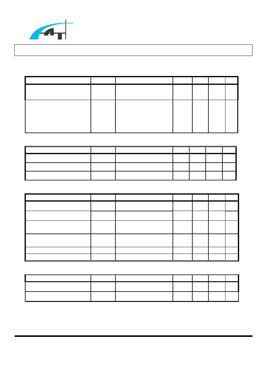
Absolute Maximum Ratings
CHARACTERISTICS SYMBOL
VALUE
UNIT
Supply Voltage
DD
V
7
V
Input Voltage (
-
IE
, DTC, SHDN)
I
V
DD
V
V
Output Voltage
O
V
DD
V +0.3
V
Output Current
O
I
120
-
/+120
mA
Operating Free-Air Temperature Range
C
T
20
-
to +85
o
C
Storage Temperature Range
storage
T
45
-
to +125
o
C
Power Dissipation
d
P
500
mW
Recommended Operating Conditions
Symbol
Min
Max
Unit
Supply Voltage,
DD
V
DD
V
2.6 6.5 V
Input Voltage, IE1, IE2
cm
V
0.3 1.5 V
Output Voltage
O
V
0
DD
V
V
Oscillator (OSC) Capacitance
OSC
C
100 15,000 pF
Oscillator (OSC) Resistance
OSC
R
3 50 k
Oscillator (OSC) Frequency
OSC
f
10 800 kHz
Output Current,
1
out
I
,
2
out
I
O
I
+50/
50
-
mA
Operating Free-Air Temperature
C
T
20
-
85
o
C
Advanced Analog Technology, Inc.
≠
≠
≠
Advanced Analog Technology, Inc
.
≠
Page 4 of 16 V 1.0
AAT1105A
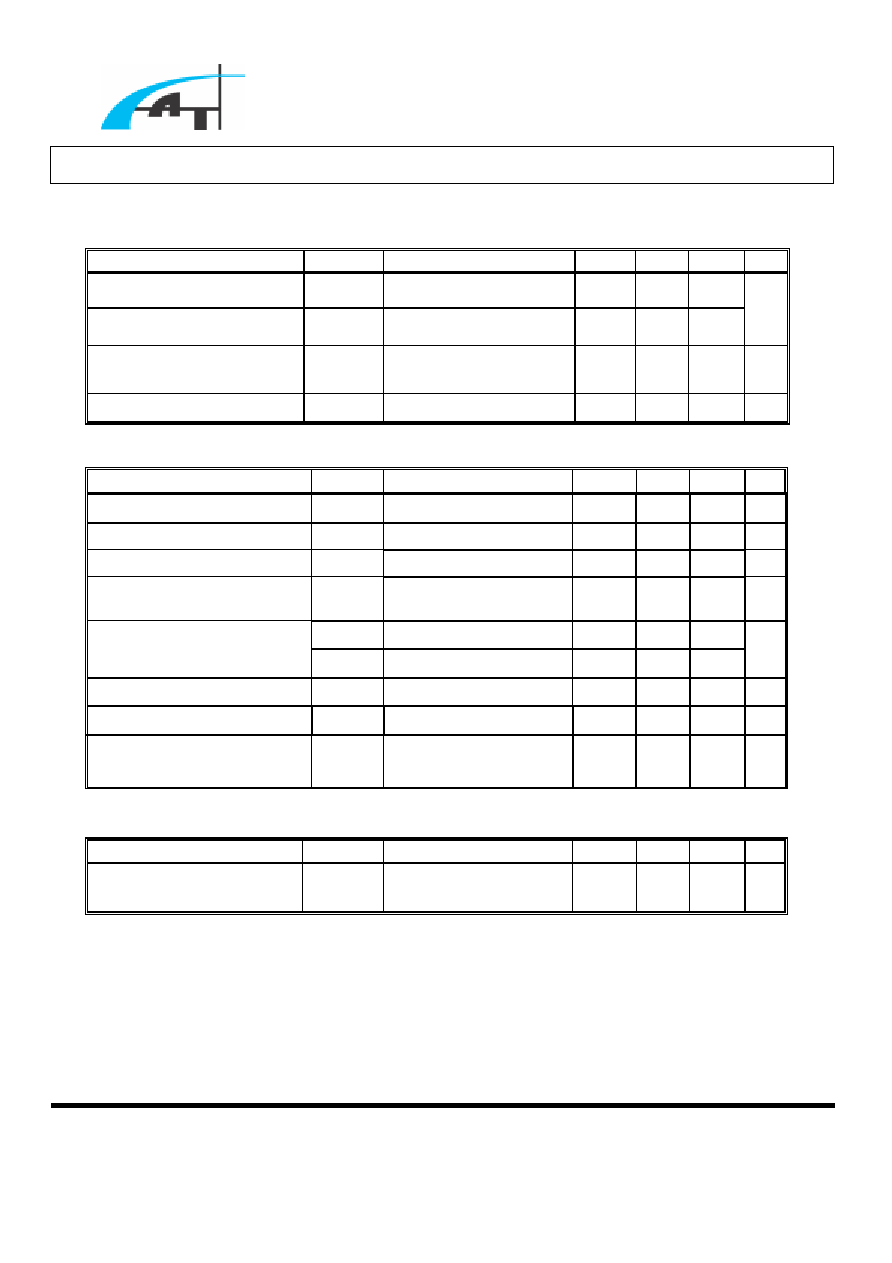
Electrical Characteristics,
DD
V = 3.3V (Unless Otherwise Specified) (See Note 1)
Oscillator
Parameter
Test Condition
Min Typ Max
Unit
Frequency
OSC
f
OSC
C
= 220pF,
OSC
R
=
5.6k
320 400 480
kHz
Frequency Changes with
DD
V
V
f
DD
V = 2.6V to 6.0V,
C
T = 25
o
C
OSC
C
= 220pF,
OSC
R
= 5.6k
- 1 -
%
Under-Voltage Protection
Parameter
Test
Condition
Min
Typ
Max
Unit
Upper Threshold Voltage
UPH
V
C
T = 25
o
C
1.81
2.03 2.25 V
Lower Threshold Voltage
UPL
V
C
T = 25
o
C
1.57
1.79 2.01 V
Hysteresis (
UPH
V
≠
UPL
V
)
HYS
V
C
T = 25
o
C
- 0.24 - V
Short Circuit Protection Control
Parameter
Test
Condition
Min
Typ
Max
Unit
Input Threshold Voltage
2
r
V
CH2 1.81
1.29
1.40
V
Input Threshold Voltage
1
r
V
CH1 0.30
0.37
0.44
V
Short-Circuit Detect
Threshold Voltage
tscd
V
0.76
0.85
0.94
V
SCP Terminal Source
Current
SCP
I
8
.
3
-
6
.
2
-
4
.
1
-
µA
Stand-by Voltage
V
STB
50 100 mV
Latch Voltage
V
LT
30 100 mV
Shutdown Control
Parameter
Test
Condition
Min
Typ
Max
Unit
Shutdown Enable Voltage
SE
V
C
T = 25
o
C
- -
0.5
V
Shutdown Release Voltage
SR
V
C
T = 25
o
C
2.0 - - V
Note 1: Typical values of all parameters are specified at
C
T =25
o
C.
Advanced Analog Technology, Inc.
≠
≠
≠
Advanced Analog Technology, Inc
.
≠
Page 5 of 16 V 1.0
AAT1105A
Electrical Characteristics,
DD
V
= 3.3V (Unless Otherwise Specified) (See Note 1) (Cont.)
Reference Voltage
Parameter
Test
Conditions
Min
Typ
Max
Unit
Internal Reference Voltage
REFi
V
mA
1
I
REF
-
=
,
C
T = 25
o
C 0.622 0.641 0.660
Reference Voltage
REF
V
mA
1
I
REF
-
=
,
C
T = 25
o
C 1.280 1.293 1.306
V
Input Voltage Regulation
RI
V
mA
1
I
REF
-
=
,
V
DD
= 2.6V to 6.0V
- 1 10
mV
Output Regulation
RO
V
mA
1
.
0
I
REF
-
=
to
1
-
mA
- 1 6
mV
EA (Error Amplifier)
Parameter
Test Condition
Min Typ Max
Unit
Input Offset Voltage
IO
V CH1,CH2, Unity Gain
-
-
6
mV
Input Bias Current
IB
I
CH1, CH2
-
±15 ±100 nA
Input Voltage Range
IR
V CH1, CH2
0.5
-
1.5
V
Open-Loop Voltage
Amplification
VO
A
70
85
-
dB
+
OS
V
1.7
2.0
-
Output Voltage Swing
-
OS
V
-
0.2
0.4
V
Output Sink Current
+
OS
I
OE=0.65V 3
10
-
mA
Output Source Current
-
OS
I
OE=0.65V -
65
-
45
-
µA
Common-Mode Rejection
Ratio
CMRR
60 80 - dB
PRDB (Power Good Protection)
Parameter
Test Condition
Min Typ Max
Unit
Low Level Output Voltage
dbl
V
Pull-High
=
k
100
R
20
- 0.2
0.4
V