
Advanced Analog Technology, Inc.
≠
≠
≠
Advanced Analog Technology, Inc
.
≠
Page 1 of 16 V 1.0
AAT1107
Details are subject to change without notice.
BUCK_BOOST & BOOST PWM CONTROLLER
WITH ADJUSTABLE LDO
FEATURES
Complete PWM Power Control Circuitry
CH1: Buck_Boost, CH2: Boost
Adjustable Low Dropout (LDO) Regulator
Under-Voltage Lockout (UVLO) Protection
Totem Pole Output
Output Short Circuit Protection
Dead Time Control : 0% to 100%
Wide Operating Frequency:
10kHz to 800kHz
PIN CONFIGURATION
1
2
3
4
5
6
7
8
16
15
14
13
12
11
10
9
IE1
OE1
DTC1
GND
OUT1
V
REF
OUT3
SCP
IE2
OE2
DTC2
OUT2
TOP VIEW
IE3
V
DD
TSSOP-16 PACKAGE
R
t
C
t
GENERAL DESCRIPTION
The AAT1107 provides an integrated two-channel
pulse-width-modulation (PWM) solution for the
power supply of DC-DC system. This device
offers system engineers the flexibility to tailor-make
the power supply circuitry for the specific
applications.
Each channel contains its own error amplifier,
PWM comparator, dead-time control (DTC) and
output driver. The two channels share common
features of under-voltage protection, oscillator,
short circuit protection and voltage reference circuit.
Two dead-time control inputs are assigned for
channel (CH1) and channel 2 (CH2) individually,
and dead-time control inputs can be used to control
on/off operation.
The AAT1107 contains one step-up (boost) circuit
at CH2 and one inverting (buck_boost) circuit at
CH1. In addition, DTC can be set to provide 0%
to 100% dead-time through a resistive divider
network and soft-start can be implemented by
paralleling the DTC resistor with a capacitor.
The Maximum output current of LDO regulator can
be enlarged by connecting an nMOSFET (or NPN
bipolar) as a source follower stage at OUT3 pin.

Advanced Analog Technology, Inc.
≠
≠
≠
Advanced Analog Technology, Inc
.
≠
Page 2 of 16 V 1.0
AAT1107
PIN DESCRIPTION
Pin No
Name I/O
Description
1
t
C
- External Timing Capacitance
2
t
R
- External Timing Resistance
3
IE3
I Inverting Input of LDO Regulator
4
IE1
I Inverting Input of Error Amplifier 1
5
OE1
O Output of Error Amplifier 1
6
DTC1
I Output 1 Dead-Time / Soft-Start Setting
7 OUT1
O
Output
1
8 GND
-
Ground
9 V
DD
-
Power
Supply
10 OUT2
O
Output
2
11
DTC2
I Output 2 Dead-Time / Soft-Start Setting
12
OE2
O Output of Error Amplifier 2
13
IE2
I Inverting Input of Error Amplifier 2
14 NE2
O
LDO
Output
15
SCP
- Timer Latch Setting
16
REF
V
O Reference Voltage (2.505V) Output
Advanced Analog Technology, Inc.
≠
≠
≠
Advanced Analog Technology, Inc
.
≠
Page 3 of 16 V 1.0
AAT1107
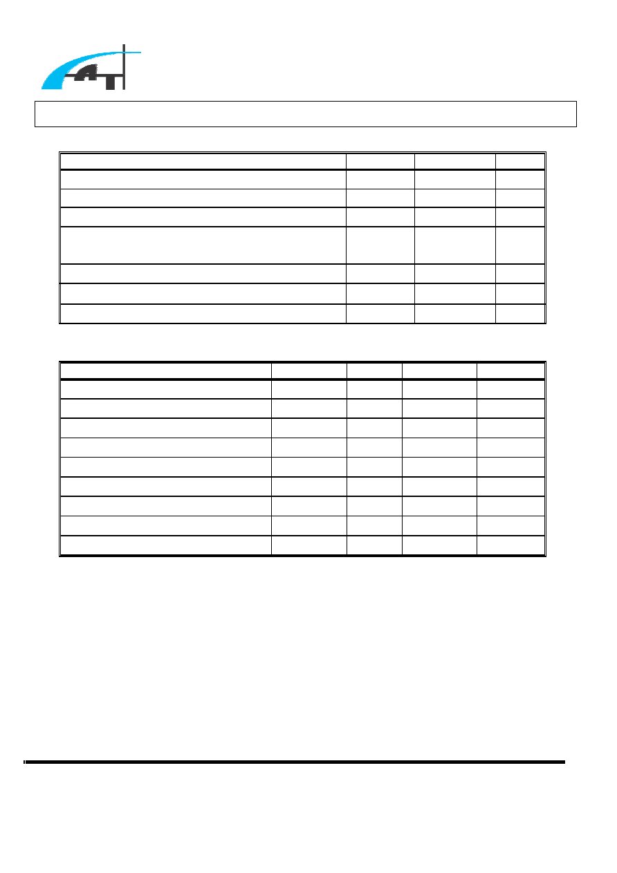
ABSOLUTE MAXIMUM RATINGS
Characteristics Symbol
Value
Unit
Supply Voltage
DD
V
7.0 V
Input Voltage (
-
IE
, DTC)
I
V
DD
V
V
Output Voltage
O
V
DD
V
+0.3
V
Output Current
O
I
120
/
120
+
-
mA
Operating Free-Air Temperature Range
C
T
20
-
to
85
+
C
o
Storage Temperature Range
storage
T
45
-
to
125
+
C
o
Power Dissipation
d
P
500
mW
RECOMMENDED OPERATING CONDITIONS
Symbol
Min
Max
Unit
Supply Voltage
DD
V
4.0 6.5 V
Input Voltage, IE1, IE2, IE3
cm
V
0.5 1.6 V
Output Voltage
O
V
0
DD
V
V
Oscillator (OSC) Capacitance
OSC
C
100 15,000
pF
Oscillator (OSC) Resistance
OSC
R
5.1 50.0
k
Oscillation (OSC) Frequency
OSC
f
10 800 kHz
Output Current,
1
OUT
I
,
2
OUT
I
12
O
I
-
50
/
50
-
+
mA
Output Current,
3
OUT
I
3
O
I
- 30 mA
Operating Free-Air Temperature
C
T
20
-
85
C
o
Advanced Analog Technology, Inc.
≠
≠
≠
Advanced Analog Technology, Inc
.
≠
Page 4 of 16 V 1.0
AAT1107
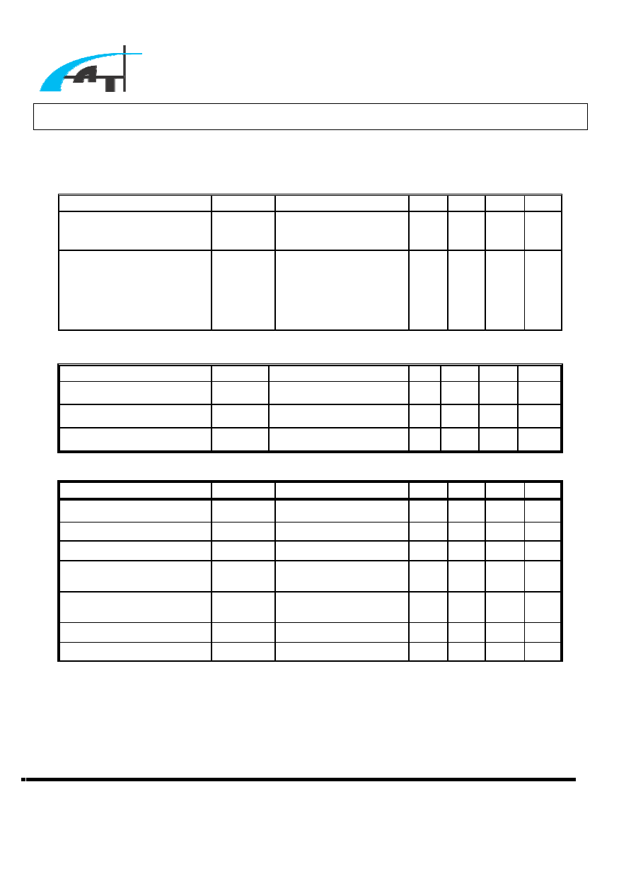
ELECTRICAL CHARACTERISTICS,
DD
V
= 5.0V (UNLESS OTHERWISE
SPECIFIED) (SEE NOTE 1)
Oscillator
Parameter
Symbol Test
Condition
Min
Typ Max Unit
Frequency
OSC
f
pF
220
C
OSC
=
,
= k
10
R
OSC
320
400 480 kHz
Frequency Change with
DD
V
V
f
6.0V
to
4.0V
V
DD
=
C
25
T
C
o
=
pF
220
C
OSC
=
= k
10
R
OSC
- 1 -
%
Under-Voltage Protection
Parameter
Symbol
Test Condition
Min Typ Max Unit
Upper Threshold Voltage
UPH
V
C
25
T
C
o
=
2.6
2.9 3.2
V
Lower Threshold Voltage
UPL
V
C
25
T
C
o
=
2.23 2.53 2.83
V
Hysteresis
(
)
UPL
UPH
V
V
-
HYS
V
C
25
T
C
o
=
- 0.37 -
V
Short Circuit Protection Control
Parameter Symbol
Test
Condition Min
Typ
Max
Unit
Input Threshold Voltage
2
r
V
CH2 2.10
2.40
2.65
V
Input Threshold Voltage
1
r
V
CH1 0.95
1.05
1.15
V
Input Threshold Voltage
3
r
V
CH3 -
1.05
-
Short-Circuit Detect
Threshold Voltage
tscd
V
1.48
1.64
1.80
V
SCP Terminal Source
Current
SCP
I
5
.
3
-
5
.
2
-
5
.
1
-
A
µ
Stand-by Voltage
STB
V
-
50
100
mV
Latch Voltage
LT
V
-
30
100
mV
Note 1: Typical values of all parameters are specified at
C
25
T
C
o
=
.
Advanced Analog Technology, Inc.
≠
≠
≠
Advanced Analog Technology, Inc
.
≠
Page 5 of 16 V 1.0
AAT1107
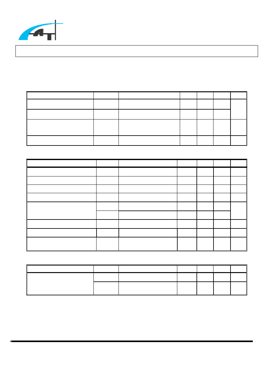
ELECTRICAL CHARACTERISTICS,
DD
V
= 5.0V (UNLESS OTHERWISE
SPECIFIED) (SEE NOTE 1) (CONT.)
Reference Voltage
Parameter Symbol
Test
Condition
Min
Typ
Max
Unit
Internal Reference Voltage
REFi
V
mA
1
I
REF
-
=
,
C
25
T
C
o
=
1.220 1.233 1.246
Reference Voltage
REF
V
mA
1
I
REF
-
=
,
C
25
T
C
o
=
2.430 2.505 2.580
V
Input Voltage Regulation
RI
V
mA
1
I
REF
-
=
,
DD
V
=4.0V to 6.0V
- 1 5
mV
Output Regulation
RO
V
mA
1
.
0
I
REF
-
=
to
mA
1
-
- 1 - mV
EA (Error Amplifier)
Parameter
Test Condition
Min Typ Max Unit
Input Offset Voltage
IO
V CH1, CH2, Unity Gain
- - 6
mV
Input Bias Current
IB
I
CH1, CH2
-
15
±
100
±
nA
Input Voltage Range
IR
V CH1, CH2
0.5
-
1.6
V
Open-Loop Voltage Gain
VO
A
70 85 - dB
+
OS
V
2.3
2.5
-
Output Voltage Swing
-
OS
V
-
0.7
0.9
V
Output Sink Current
+
OS
I
OE=1.25V 3
20
-
mA
Output Source Current
-
OS
I
OE=1.25V -
75
-
45
-
A
µ
Common-Mode Rejection
Ratio
CMRR
60 80 - dB
Operating Current
Parameter
Test Condition
Min Typ Max Unit
OFF
DD
I
-
Output "OFF" State
-
1.8
-
mA
Supply Current
ON
DD
I
-
= k
10
R
OSC
- 2.0 -
mA