 | –≠–ª–µ–∫—Ç—Ä–æ–Ω–Ω—ã–π –∫–æ–º–ø–æ–Ω–µ–Ω—Ç: AAT1108 | –°–∫–∞—á–∞—Ç—å:  PDF PDF  ZIP ZIP |

Advanced Analog Technology, Inc.
≠
≠
Advanced Analog Technology, Inc
. V 0.1
AAT1108
Preliminary and Provisional
2-CHANNEL STEP-UP PWM CONTROLLERS
WITH ADJUSTABLE LDO
Features
Complete PWM Power Control Circuitry
Adjustable LDO Regulator
Under-voltage Lockout Protection
Totem pole Output
Output Short Circuit Protection
Dead Time Control0 to 100%
Wide Operating Frequency
10kHz to 800kHz
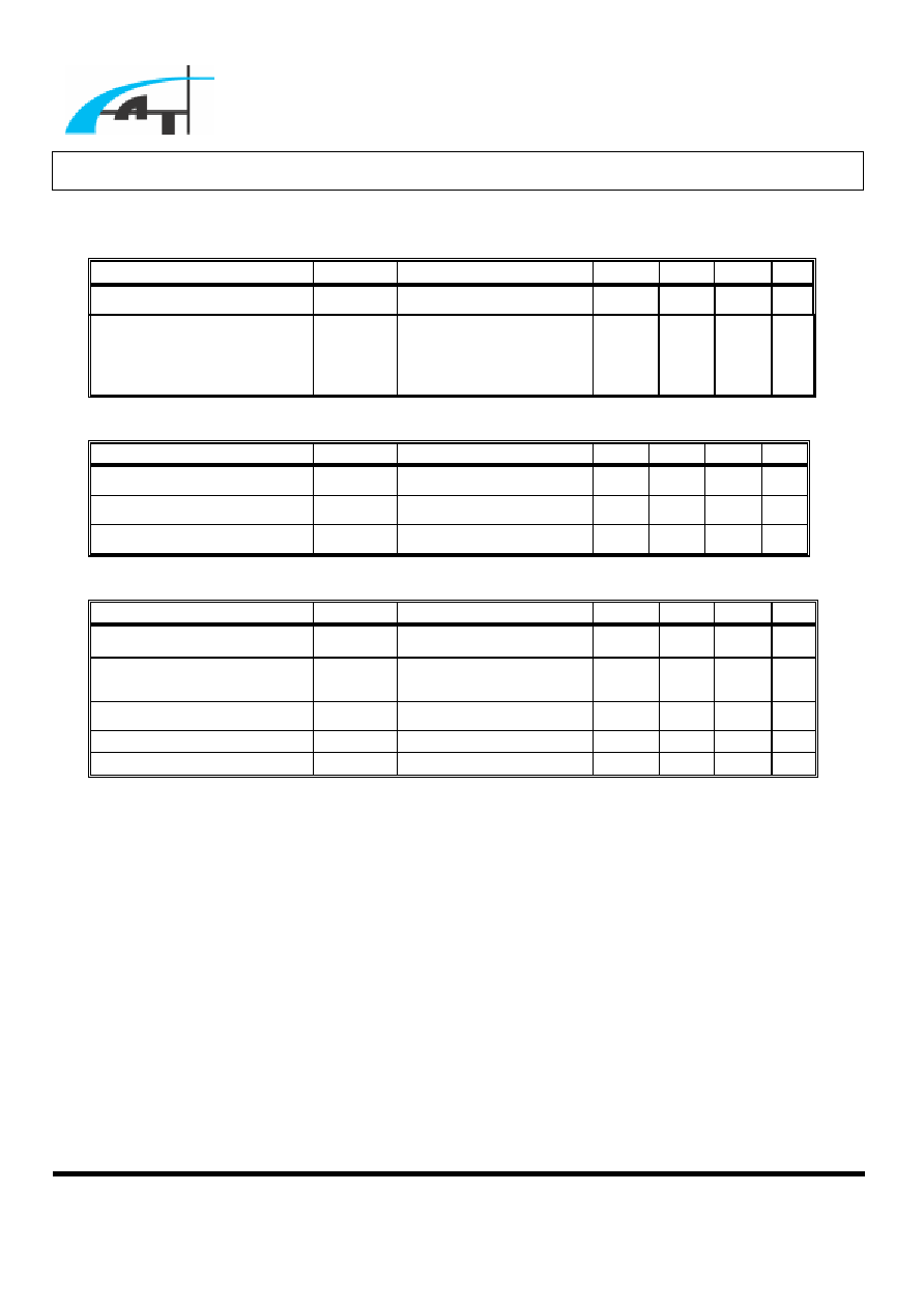
Pin Configuration
1
2
3
4
5
6
7
8
16
15
14
13
12
11
10
9
RT
INV1
FB1
DTC1
GND
OUT1
Vref
OUT3
SCP
INV2
FB2
DTC2
OUT2
TOP VIEW
(TSSOP-16 PACKAGE)
DD
V
INV3
CT
General Description
The AAT1108 series provides an integrated
two-channel pulse-width-modulation (PWM)
solution for the power supply of DC-DC system,
this device offers the systems engineer the
flexibility to tailor the power supply circuitry to a
specific application. Each channel contains its own
error amplifier, PWM comparator, dead≠time
control and output driver. The under-voltage
protection, oscillator, short circuit protection and
voltage reference circuit are common for the two
channels.
The AAT1108 contains two boost (step-up)
exclusive circuits. Dead-time control (DTC) can be
set to provide 0% to 100% dead time by resistive
divider network. Soft start can be implemented by
paralleling the DTC resistor with a capacitor. Two
dead time control inputs are assigned for Ch-1 and
Ch-2 individually, and dead time control inputs can
be used to control on / off operation.
The maximum output currents of LDO regulator
can be enlarged by connect a N_MOS FET (or NPN
bipolar) as a source follow stage at out3 pin.
*Spec is subject to change without notice in this document.

Advanced Analog Technology, Inc.
≠
≠
Advanced Analog Technology, Inc
. V 0.1
AAT1108
Pin Description
Pin # Name I/O
Description
1
CT
I External timing capacitance
2
RT
I External timing resistance
3 INV3 I
Negative input for LDO amplifier
4 INV1 I
Negative input for error amplifier 1
5
FB1
I Output for error amplifier 1
6
DTC1
I Output 1 dead time / soft start setting
7 OUT1 O
Output
1
8 GND
Ground
9 V
DD
I
Power
supply
10
OUT2 O Output 2
11
DTC2
I Output 2 dead time / soft start setting
12
FB2
I Output for error amplifier 2
13
INV2
I Negative input for error amplifier 2
14
OUT3 I LDO output
15
SCP
I Timer latch setting
16
V
ref
O Reference voltage (2.505V) output

Advanced Analog Technology, Inc.
≠
≠
Advanced Analog Technology, Inc
. V 0.1
AAT1108
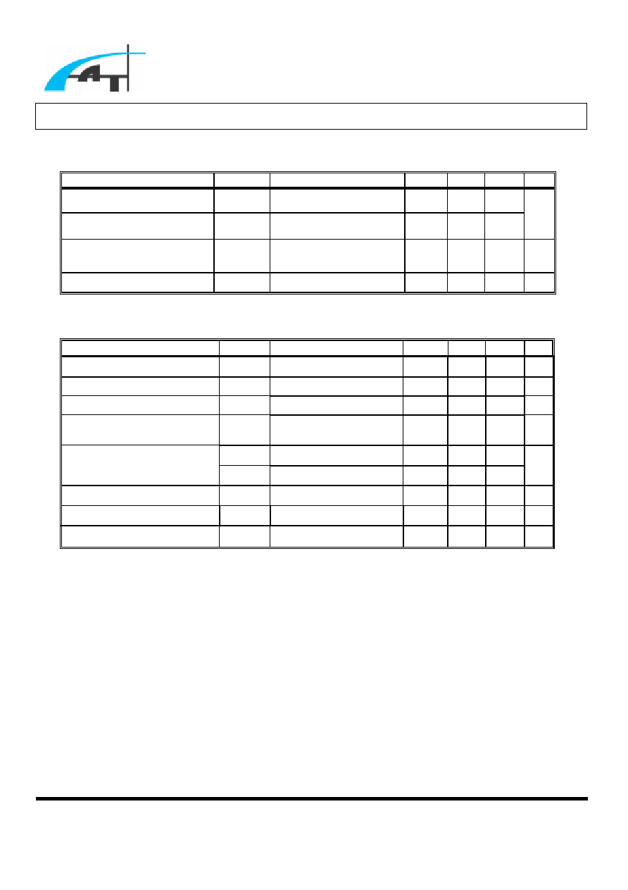
Absolute Maximum Ratings
CHARACTERISTICS SYMBOL
VALUE
UNIT
Supply voltage
DD
V
7 V
Input voltage (IN-, DTC)
I
V
DD
V
V
Output voltage
O
V
DD
V +0.3
V
Output current
O
I
-120/+120 mA
Operating free-air temperature range
ope
T
-20 to 85
o
C
Storage temperature range
stg
T
-65 to 150
o
C
Power dissipation
Pd
500
mW
Recommended Operating Conditions
Symbol
Min
Max
Unit
Supply voltage,
DD
V
DD
V
4.0 6.5 V
Input voltage, INV1, INV2, INV3
V
cm
0.5 1.6 V
Output voltage
O
V
0
DD
V
V
OSC capacitor
T
C
100 15000 pF
OSC resistor (Note 1)
T
R
5.1 50 k
Oscillator frequency
OSC
f
10 800 kHz
Output current, Iout1, Iout2
2
O
I
+50/-50 mA
Out put current, Iout3 (Vout3 = 3.3v)
3
O
I
+30 mA
Operating free-air temperature
ope
T
-20 85
o
C
Advanced Analog Technology, Inc.
≠
≠
Advanced Analog Technology, Inc
. V 0.1
AAT1108
Electrical Characteristics,
DD
V = 5.0V (Unless Otherwise Specified) (See Note 1)
Oscillator
Parameter
Test Condition
Min Typ Max
Unit
Frequency
OSC
f
T
C = 220pF,
T
R = 10k
320 400 480
KHz
Frequency change with
DD
V
dV
f
DD
V = 4.0V to 6.0V,
A
T = 25
o
C
T
C = 220pF,
T
R = 10k
1
%
Under-voltage Protection
Parameter
Test
Condition
Min
Typ
Max
Unit
Upper threshold voltage
UPH
V
A
T = 25
o
C
2.6 2.9 3.2 V
Lower threshold voltage
UPL
V
A
T = 25
o
C
2.23
2.53 2.83 V
Hysteresis (
UPH
V
≠
UPL
V
)
HYS
V
A
T = 25
o
C
0.37 V
Short Circuit Protection Control
Parameter
Test
Condition
Min
Typ
Max
Unit
Input threshold voltage
1
r
V
Ch-1, 2
2.1
2.4
2.65
V
Short-circuit detect threshold
voltage
2
r
V
1.48
1.64
1.8
V
SCP terminal source current
SCP
I
-1.5
-2.5
-3.5
µA
Standy Voltage
V
STB
50 100 mV
Latch Voltage
V
LT
30 100 mV
Note1: Typical values of all parameters are specified at
A
T
=25
o
C.
Advanced Analog Technology, Inc.
≠
≠
Advanced Analog Technology, Inc
. V 0.1
AAT1108
Electrical Characteristics,
DD
V = 5.0V (Unless Otherwise Specified) (See Note 1) (continued)
Reference Voltage
Parameter
Test
Conditions
Min
Typ
Max
Unit
Internal reference Voltage
V
refi
mA
1
I
REF
-
=
,
A
T = 25
o
C 1.220 1.233 1.246
Reference voltage
REF
V
mA
1
I
REF
-
=
,
A
T = 25
o
C 2.430 2.505 2.580
V
Input voltage regulation
RI
V
mA
1
I
REF
-
=
,
V
DD
= 4.0V to 6.0V
1 5
mV
Output regulation
RO
V
mA
1
.
0
I
REF
-
=
to -1mA
1
mV
EA (Error Amplifier)
Parameter
Test Condition
Min Typ Max
Unit
Input offset voltage
IO
V Ch-1,2, A
V
=1
6
mV
Input bias current
IB
I
Ch-1,2
±15
±100
nA
Input voltage range
IR
V Ch-1,2 0.5
1.6
V
Open-loop voltage
amplification
VD
A
70
85
dB
+
OM
V
2.3
2.5
Output voltage swing
-
OM
V
0.7
0.9
V
Output sink current
+
OM
I
FB=1.25V 3
20
mA
Output source current
-
OM
I
FB=1.25V -45
-75
µA
Common-mode rejection ratio CMRR
60 80 dB