 | –≠–ª–µ–∫—Ç—Ä–æ–Ω–Ω—ã–π –∫–æ–º–ø–æ–Ω–µ–Ω—Ç: AAT1118A | –°–∫–∞—á–∞—Ç—å:  PDF PDF  ZIP ZIP |

≠
∞ " ~ H ] ∂ þ
¯
≠
≠
≠
Page 1 of 18 V 1.0
AAT1118/A/B
Details are subject to change without notice.
ADJUSTABLE TRIPLE-CHANNEL TFT LCD
DC-DC CONVERTER
Features
Built in 1.6A, 0.2 Switching NMOS
Fault and Thermal Protection
Internal Soft-Start Function
Internal Power Up Sequencing
Dual Adjustable Charge Pump Output
Positive Output to 40V
Negative Output to 40V
-
Power Good Output
TSSOP-16 Package
Pin Configuration
(Top View)
General Description
The AAT1118/A/B is an adjustable triple-channel
TFT LCD DC-DC converter that provides one
current mode PWM, one positive charge pump and
one negative charge pump. Built-in functions
include soft-start and power up sequencing. When
power is turned on, soft-start avoids inrush current.
Power
up
sequencing
feature
provides
compensation for LCD panel to maintain a smooth
voltage during a turn-on cycle.
The DC-DC converter consists of an on-chip
voltage reference, error amplifier, current sense,
pulse width modulation controller, under-voltage
lockout protection, thermal detect, soft-start, and
fault protection circuit.
When the two charge pumps are in operation, the
output voltage would be doubled and the generated
VP3 and VP2 (Note 1) could switch on or off TFT
gate.
With the minimal external components, the
AAT1118/A/B offers a simple and economical
solution for TFT LCD power.
Note 1: Please refer to page 13 and 14 for VP3 and
VP2.
(TSSOP-16 Package)
AAT1118/A/B
1
2
3
4
5
6
7
8
9
10
11
12
13
14
15
16
PGO
IN1
EO
GND
IN3
IN2
GND1
SW
GND2
/
OUT3
OUT2
SHDN
DD
V
DD1
V
REF
V
DD2
V
CH3
V
AAT1118/A/B
1
2
3
4
5
6
7
8
9
10
11
12
13
14
15
16
PGO
IN1
EO
GND
IN3
IN2
GND1
SW
GND2
/
OUT3
OUT2
SHDN
DD
V
DD1
V
REF
V
DD2
V
CH3
V

≠
∞ " ~ H ] ∂ þ
¯
≠
≠
≠
Page 2 of 18 V 1.0
AAT1118/A/B
Pin Description
PIN NO. NAME I/O
DESCRIPTION
1
PGO
O HV Switch Output
2
IN1
I
Inverting Input Pin of PWM Error Amplifier
3
EO
I
Output Pin of PWM Error Amplifier
4
DD
V
-
Power Supply
5
GND
-
Ground
6
REF
V
O Reference Voltage Output
7
IN3
I
Charge Pump Channel 3 Feedback Input
8
IN2
I
Charge Pump Channel 2 Feedback Input
9
SHDN
I
Shutdown Control Pin; High for Enable
10
OUT2
O Charge Pump Channel 2 Output
11
DD1
V
-
High Voltage Power Supply
12
OUT3
O Charge Pump Channel 3 Output
DD2
V
-
High Voltage Power Supply
13
CH3
V
O Power Output for Channel 3 (AAT1118B Only)
14
GND2
-
Ground
15
SW
O Switch Pin
16
GND1
-
SW MOS Ground
≠
∞ " ~ H ] ∂ þ
¯
≠
≠
≠
Page 3 of 18 V 1.0
AAT1118/A/B
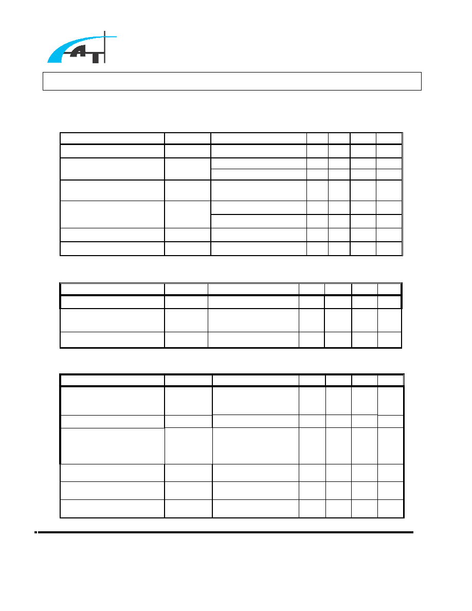
Absolute Maximum Ratings
PARAMETER
SYMBOL
VALUE
UNIT
DD
V
to GND
DD
V
7
V
SW to GND
SW
V
18
V
DD1
V
,
DD2
V
to GND
DDH
V
16
V
Input Voltage 1 (IN1, IN2, IN3, SHDN)
V
I1
DD
V +0.3
V
Output Voltage 1 (EO,
REF
V
)
O1
V
DD
V
+0.3
V
Output Voltage 2 (OUT2, OUT3, SW, PGO)
O2
V
DDH
V
+0.3
V
Operating Free-Air Temperature Range
C
T
40
-
to 85
+
C
Storage Temperature Range
storage
T
45
-
to 125
+
C
Power Dissipation
d
P
750
mW
≠
∞ " ~ H ] ∂ þ
¯
≠
≠
≠
Page 4 of 18 V 1.0
AAT1118/A/B
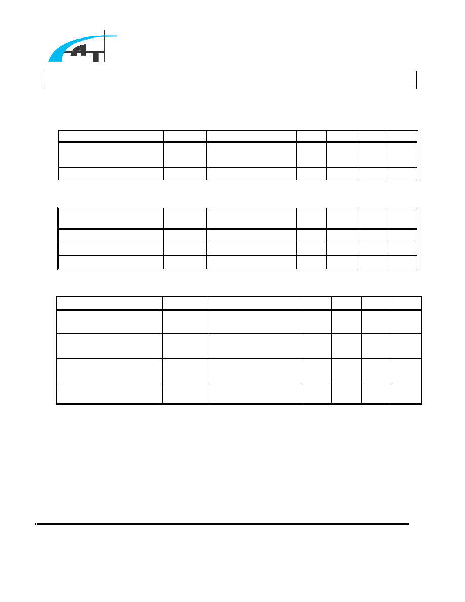
Electrical Characteristics, V
DD
= 3.3V, V
DDH
= 10V
Operating Power
PARAMETER
SYMBOL
TEST CONDITION MIN TYP MAX UNIT
Input Supply Voltage Range
DD
V
2.6
5.5
V
Falling
2.1 2.2
2.3
V
VDD Under Voltage Lockout
UVLO
V
Rising
2.3 2.4
2.5
V
Regulated Output Voltage
Range
P1
V
6
14
V
IN1
V =1.3V, not switching
0.5
0.8
mA
Quiescent Current
VDD
I
IN1
V =1.1V, switching
3
6
mA
Shutdown Current
SHDN
I
SHDN
V
=GND
0.1 10.0
A
Thermal Shutdown
160
C
Reference Voltage
PARAMETER
SYMBOL TEST CONDITION MIN TYP MAX UNIT
Reference Voltage
REF
V
I
Vref
= 100µA
1.238 1.250 1.262 V
Line Regulation
RI
V
I
Vref
= 100µA,
DD
V
=2.5V~5V
-
2
5
mV
Load Regulation
RO
V
I
Vref
= 0~100µA
-
1
5
mV
EA (Error Amplifier)
PARAMETER
SYMBOL TEST CONDITION MIN TYP MAX UNIT
Feedback Voltage
IN1
V
l
l
EO
V = ~ ` Ø ÿ
1.238 1.250 1.262
V
Input Bias Current
1
B
I
V
IN1
=1.24V
0
40
nA
Feedback-Voltage Line
Regulation
RI
V
l
l
l
EO
V
= ~ ` Ø ÿ
Ø`
ÿ
DD
V
® ` ® ÿ
0.05 0.15 % /V
Transconductance
m
g
I=5 A
70
105
240
A /V
Voltage Gain
V
A
1,500
V /V
Fault Detect Trigger Voltage
FI
V
1.07 1.10 1.14
V
≠
∞ " ~ H ] ∂ þ
¯
≠
≠
≠
Page 5 of 18 V 1.0
AAT1118/A/B
Electrical Characteristics, V
DD
= 3.3V, V
DDH
= 10V
Oscillator
PARAMETER
SYMBOL TEST CONDITION
MIN TYP MAX UNIT
Oscillation Frequency
OSC
f
1,100 1,320 1,600
kHz
Maximum Duty Cycle
MAX
D
79
85
92
%
N-Channel Switch
PARAMETER
SYMBOL
TEST CONDITION
MIN TYP MAX UNIT
Current Limit
LIM
I
1.1
1.6
2.1
A
On-Resistance
ON
R
SW
I =1.2A
0.28
0.50
L
Leakage Current
SWOFF
I
SW
V =12V
0.01
20.00
A
Control Inputs Characteristics
PARAMETER
SYMBOL
TEST CONDITION
MIN TYP MAX UNIT
Input Low Voltage
IL
V
0.3
DD
V
V
Input High Voltage
IH
V
0.7
DD
V
V
Hysteresis
HYS
V
0.1
DD
V
V
SHDN Pull Up Current
PH
I
0.001 1.000
A