 | –≠–ª–µ–∫—Ç—Ä–æ–Ω–Ω—ã–π –∫–æ–º–ø–æ–Ω–µ–Ω—Ç: AAT1501A | –°–∫–∞—á–∞—Ç—å:  PDF PDF  ZIP ZIP |
Advanced Analog Technology, Inc.
≠
≠
≠
Advanced Analog Technology, Inc
.
≠
Page 1 of 10 V1.0
AAT1501/A
Details are subject to change without notice
REGULATED CHARGE PUMP DC/DC CONVERTERS
Features
Monitored Output Voltage
(AAT1501:
%
4
V
5
V
O
±
=
)
(AAT1501A:
%
4
V
5
.
4
V
O
±
=
)
Output Current: 120mA (
DD
V = 3.3V)
150mA (
DD
V = 3.6V)
Input Voltage Range: 2.7V to 5.0V
A Power-Saving Shutdown Current of less than
A
1
µ
Internal Oscillation Frequency : 750kHz
Compact SOT-23-6 Package
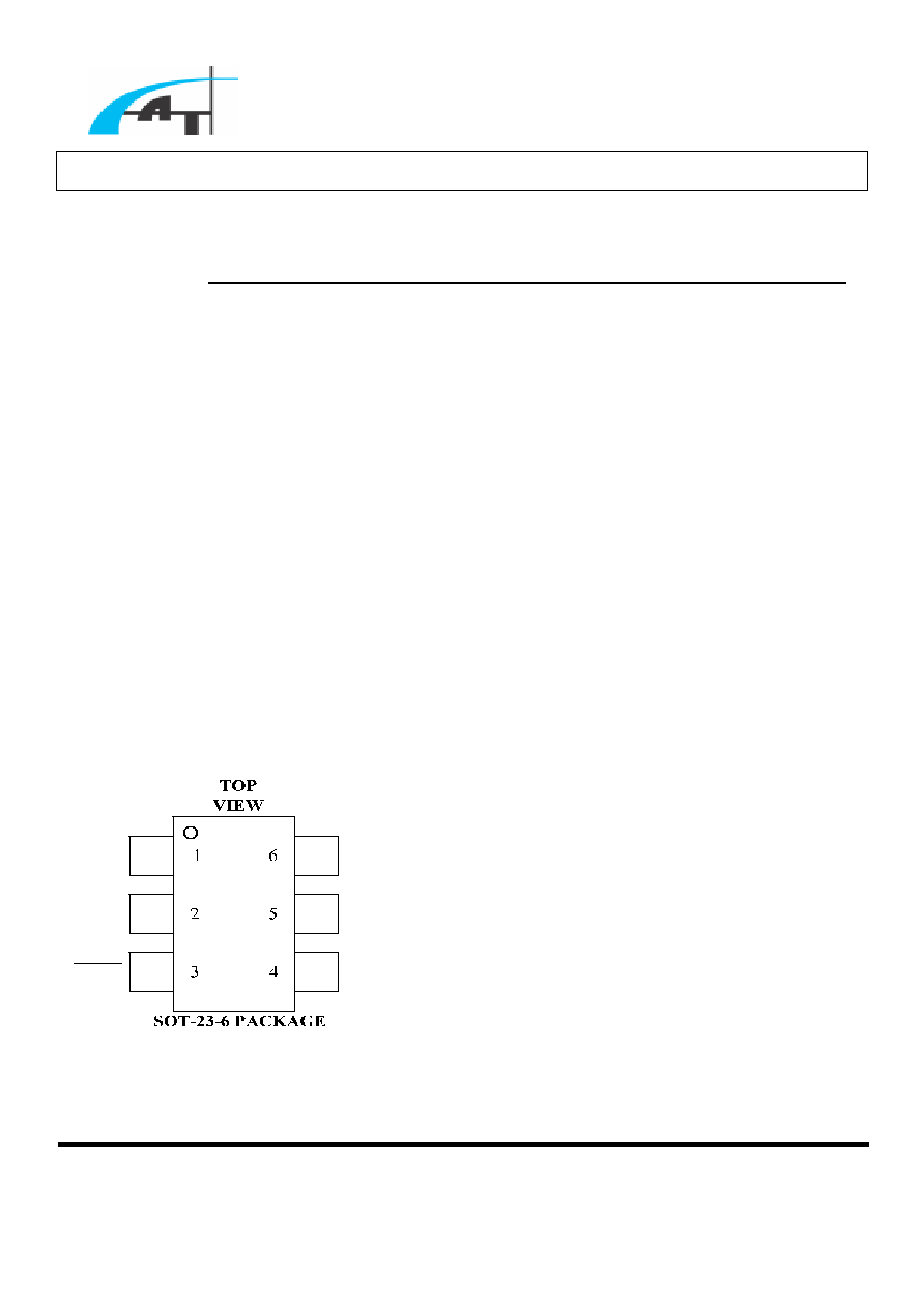
Pin Configuration
O
V
DD
V
-
F
C
+
F
C
GND
SHDN
General Description
The AAT1501/A is a charge pump DC/DC
converter mainly used for white LED backlighting.
It operates with an input voltage ranging from 2.7V
to 5.0V to generate constant 5.0V (AAT1501) or
4.5V (AAT1501A) output. The regulated output is
produced by using an internal feedback switched
capacitor voltage doublers.
The AAT1501/A requires no external inductor
when operating. By using a flying capacitor, the
AAT1501/A can deliver up to 120mA (
DD
V = 3.3V)
output current for the system.
The AAT1501/A's
typical ultra low operating current, and compact
external parts make it an ideal component for small,
portable, battery-powered applications.
AAT1501/A comes in a compact 6-pin SOT-23
package to offer users optimal and economical
power management solution.
Advanced Analog Technology, Inc.
≠
≠
≠
Advanced Analog Technology, Inc
.
≠
Page 2 of 10 V1.0
AAT1501/A
Pin Description
Pin No Name I/O
Description
1
O
V
O Output Voltage
2 GND
-
Ground
3
SHDN I Shutdown Input Pin
4
-
F
C O Flying Capacitor Negative Terminal
5
DD
V
- Supply Voltage
6
+
F
C
I Flying Capacitor Positive Terminal
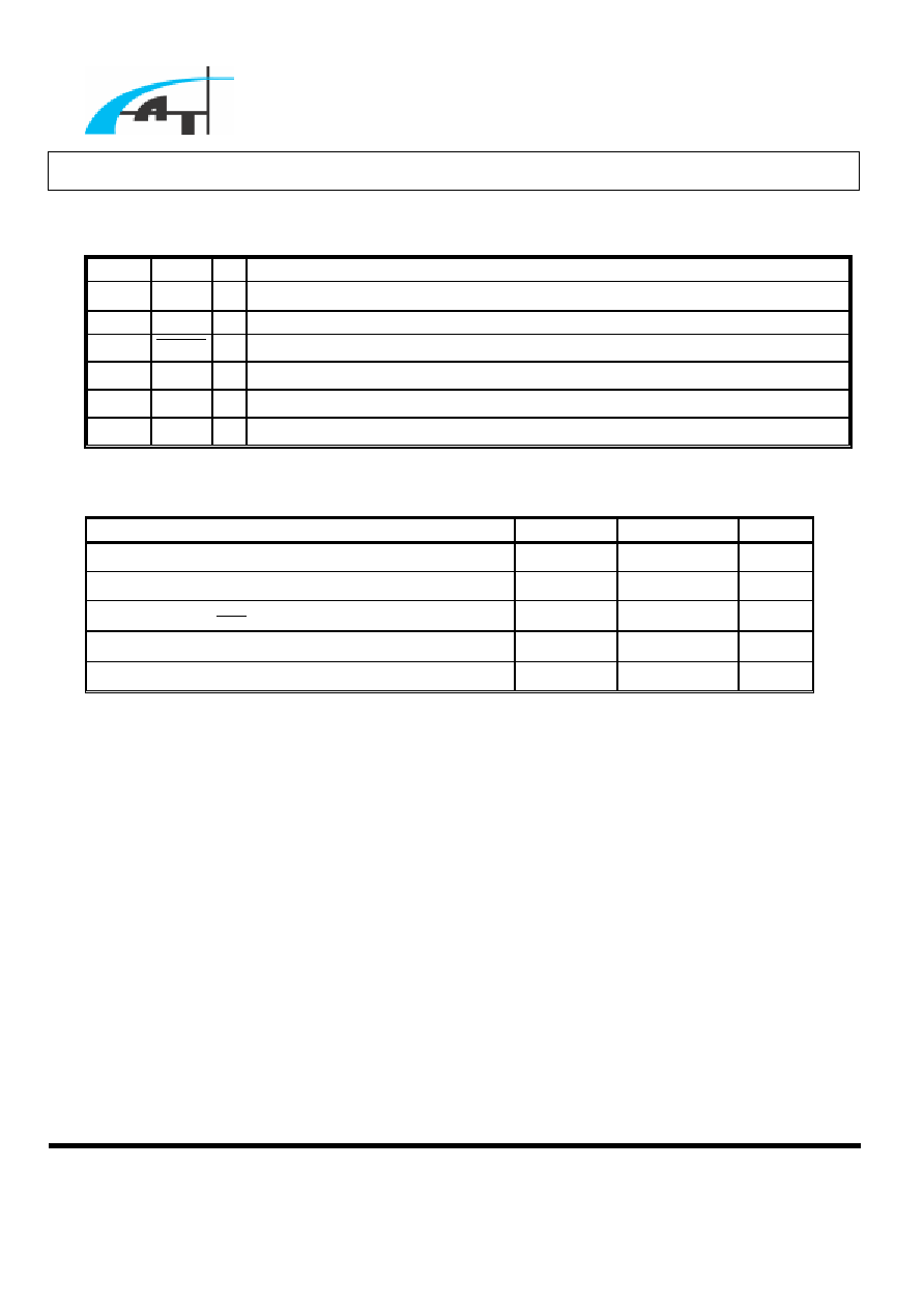
Absolute Maximum Ratings
CHARACTERISTICS SYMBOL
VALUE
UNIT
Supply Voltage
DD
V
6 V
Output Voltage (
O
V ,
+
CF
V
,
-
CF
V
)
O
V
6 V
Input Voltage (
SHDN
V
)
I
V
6 V
Storage Temperature Range
storage
T
45
-
to 125
o
C
Operating Temperature Range
C
T
40
-
to 85
o
C
Advanced Analog Technology, Inc.
≠
≠
≠
Advanced Analog Technology, Inc
.
≠
Page 3 of 10 V1.0
AAT1501/A
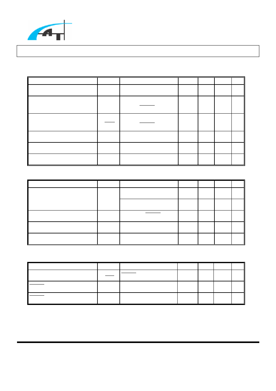
Electrical Characteristics,
DD
V
= 3.3 V (Unless Otherwise Specified)
Operating Condition
Parameter
Symbol
Test Condition
Min Typ Max Unit
Supply Voltage
DD
V 2.7
5.0
V
Supply Current
DD
I
DD
V
=2.7V to 5.0V,
O
I =0 ,
DD
V
SHDN
=
- 1.5
2.0
mA
Shutdown Current
SHDN
I
DD
V
=2.7V to 5.0V,
O
I =0 ,
V
0
SHDN
=
- 0.01
1.00
A
µ
Oscillation Frequency
OSC
f
-
750
-
kHz
Thermal Shutdown
T
SHDN
-
160
-
∫C
Thermal Shutdown Hysteresis T
HYS
-
20
- ∫C
Output Performance
Parameter
Symbol
Test Condition
Min Typ Max Unit
AAT1501 4.8
5.0
5.2
V
Output Voltage
OUT
V
AAT1501A 4.3
4.5
4.7
V
Output Current
O
I
DD
V =3V,
DD
V
SHDN
=
80 - -
mA
Output Ripple
OR
V
DD
V =3V,
O
I =50mA
- 50 -
mV
Efficiency
DD
V =2.7V,
O
I =30mA
- 83 - %
Control Input
Parameter
Symbol
Test Condition
Min Typ Max
Unit
Input Current
SHDN
I
SHDN = 0 ~ V
DD
- ±0.1
±1
µA
SHDN High Voltage
IH
V
1.1
V
SHDN Low Voltage
IL
V
0.5
V
Advanced Analog Technology, Inc.
≠
≠
≠
Advanced Analog Technology, Inc
.
≠
Page 4 of 10 V1.0
AAT1501/A
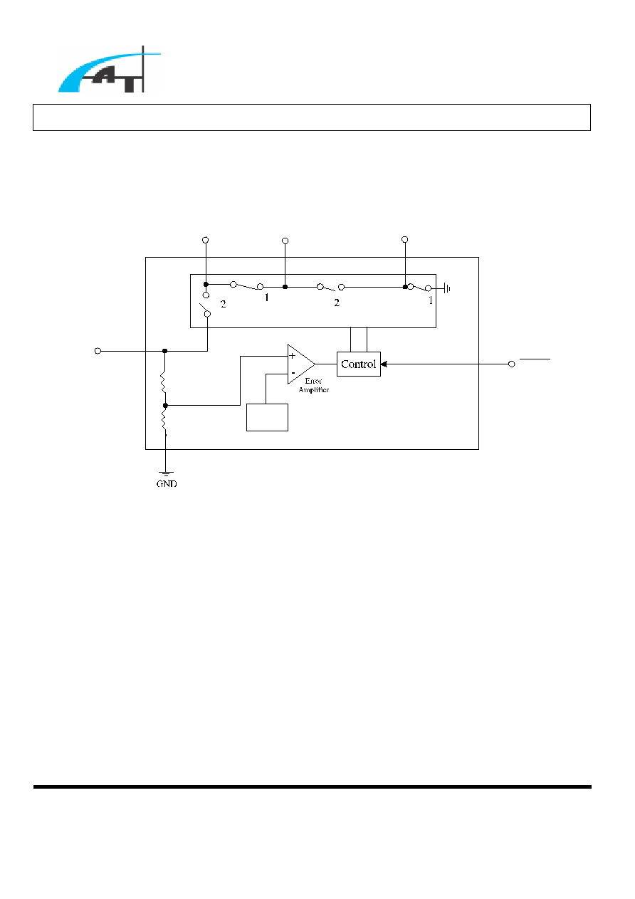
Block Diagram
REF
V
DD
V
+
F
C
-
F
C
SHDN
O
V

Advanced Analog Technology, Inc.
≠
≠
≠
Advanced Analog Technology, Inc
.
≠
Page 5 of 10 V1.0
AAT1501/A
Application Circuit
DD
V
-
F
C
+
F
C
SHDN
O
V
FLY
C
GND
O
V
DD
V
IN
C
F
10
µ
F
1
µ
O
C
F
10
µ