
ABB Semiconductors AG reserves the right to change specifications without notice.
V
DRM
=
4500 V
I
TGQM
=
2000 A
I
TSM
=
13 kA
V
T0
=
1.80 V
r
T
=
0.85 m
V
DClin
=
2200 V
Gate turn-off Thyristor
5SGA 20H4502
Doc. No. 5SYA 1210-01 Aug. 2000
�
Patented free-floating silicon technology
�
Low on-state and switching losses
�
Annular gate electrode
�
Industry standard housing
�
Cosmic radiation withstand rating
Blocking
V
DRM
Repetitive peak off-state voltage
4500
V
V
GR
2V
V
RRM
Repetitive peak reverse voltage
17
V
I
DRM
Repetitive peak off-state current
100
mA
V
D
= V
DRM
V
GR
2V
I
RRM
Repetitive peak reverse current
50
mA
V
R
= V
RRM
R
GK
=
V
DClink
Permanent DC voltage for 100
FIT failure rate
2200
V
-40
T
j
125 �C. Ambient cosmic
radiation at sea level in open air.
Mechanical data
(see Fig. 19)
min.
17 kN
F
m
Mounting force
max.
24 kN
A
Acceleration:
Device unclamped
Device clamped
50
200
m/s
2
m/s
2
M
Weight
0.8 kg
D
S
Surface creepage distance
22 mm
D
a
Air strike distance
13 mm

5SGA 20H4502
ABB Semiconductors AG reserves the right to change specifications without notice.
Doc. No. 5SYA 1210-01 Aug. 2000
page 2 of 9
GTO Data
On-state
I
TAVM
Max. average on-state current
710 A
Half sine wave, T
C
= 85 �C
I
TRMS
Max. RMS on-state current
1115 A
I
TSM
13 kA
t
P
=
10 ms
T
j
=
125�C
Max. peak non-repetitive
surge current
24 kA
t
P
=
1 ms
After surge:
I
2
t
Limiting load integral
0.85
10
6
A
2
s
t
P
=
10 ms
V
D
= V
R
= 0V
0.29
10
6
A
2
s
t
P
=
1 ms
V
T
On-state voltage
3.50 V
I
T
=
2000 A
V
T0
Threshold voltage
1.80 V
I
T
=
400 - 3000 A
T
j
=
125 �C
r
T
Slope resistance
0.85 m
I
H
Holding current
50 A
T
j
= 25 �C
Gate
V
GT
Gate trigger voltage
1.0
V
V
D
= 24 V
T
j
=
25 �C
I
GT
Gate trigger current
2.5
A
R
A
= 0.1
V
GRM
Repetitive peak reverse voltage
17
V
I
GRM
Repetitive peak reverse current
50
mA
V
GR
= V
GRM
Turn-on switching
di/dt
crit
Max. rate of rise of on-state
400 A/�s
f = 200Hz
I
T
= 2000 A,
T
j
= 125 �C
current
600 A/�s
f = 1Hz
I
GM
= 30 A, di
G
/dt = 20 A/�s
t
d
Delay time
2.0 �s
V
D
=
0.5 V
DRM
T
j
=
125 �C
t
r
Rise time
6.0 �s
I
T
=
2000 A
di/dt =
200 A/�s
t
on(min)
Min. on-time
80 �s
I
GM
=
30 A
di
G
/dt =
20 A/�s
E
on
Turn-on energy per pulse
2.50 Ws
C
S
=
4 �F
R
S
=
5
Turn-off switching
2000 A
V
DM
= V
DRM
di
GQ
/dt =
30 A/�s
I
TGQM
Max controllable turn-off
current
C
S
= 4 �F
L
S
0.3 �H
t
s
Storage time
22.0 �s
V
D
= � V
DRM
V
DM
=
V
DRM
t
f
Fall time
3.0 �s
T
j
=
125 �C di
GQ
/dt =
30 A/�s
t
off(min)
Min. off-time
80 �s
I
TGQ
= I
TGQM
E
off
Turn-off energy per pulse
7.5 Ws
C
S
=
4 �F R
S
=
5
I
GQM
Peak turn-off gate current
725 A
L
S
0.3 �H
5SGA 20H4502
ABB Semiconductors AG reserves the right to change specifications without notice.
Doc. No. 5SYA 1210-01 Aug. 2000
page 3 of 9
Thermal
T
j
Storage and operating
-40...125�C
junction temperature range
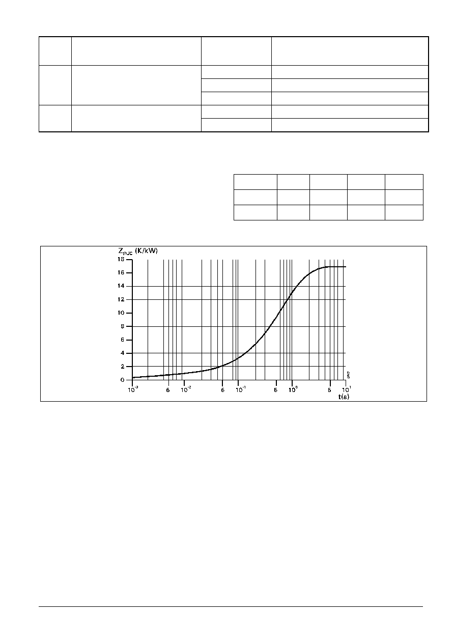
R
thJC
Thermal resistance
30
K/kW
Anode side cooled
junction to case
39
K/kW
Cathode side cooled
17
K/kW
Double side cooled
R
thCH
Thermal resistance case to
10
K/kW
Single side cooled
heat sink
5
K/kW
Double side cooled
i
1
2
3
4
R
I
(K/kW)
11.7
4.7
0.64
0.0001
Analytical function for transient thermal
impedance:
)
e
-
(1
R
=
(t)
Z
4
1
i
/
t
-
thJC
i
=
i
i
(s)
0.9
0.26
0.002
0.001
Fig. 1
Transient thermal impedance, junction to case.
5SGA 20H4502
ABB Semiconductors AG reserves the right to change specifications without notice.
Doc. No. 5SYA 1210-01 Aug. 2000
page 4 of 9
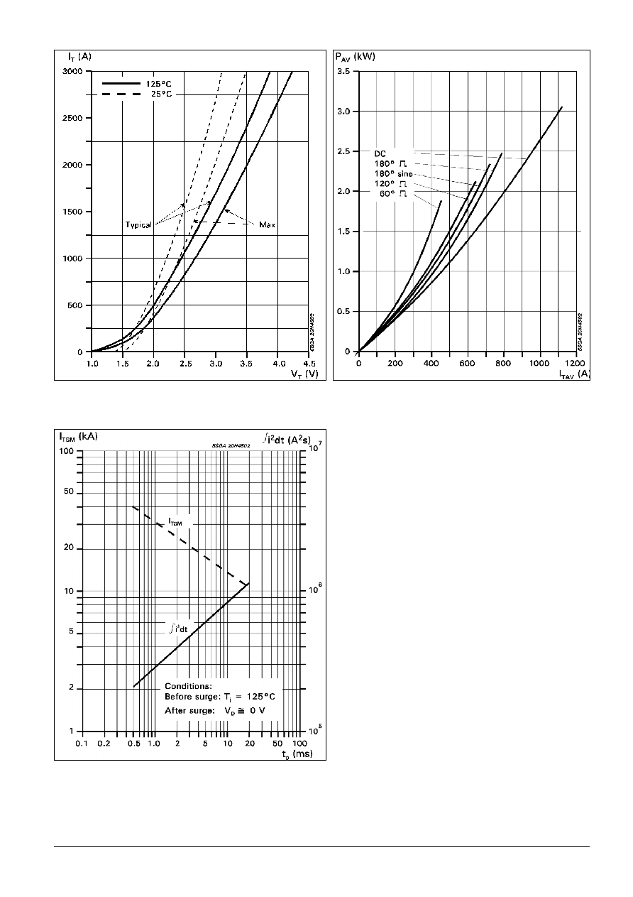
Fig. 2
On-state characteristics
Fig. 3
Average on-state power dissipation vs.
average on-state current.
Fig. 4
Surge current and fusing integral vs. pulse
width

5SGA 20H4502
ABB Semiconductors AG reserves the right to change specifications without notice.
Doc. No. 5SYA 1210-01 Aug. 2000
page 5 of 9
Fig. 5
Forward blocking voltage vs. gate-cathode
resistance.
Fig. 6 Static dv/dt capability: Forward blocking
voltage vs. neg. gate voltage or gate
cathode resistance.
Fig. 7 Forwarde gate current vs. forard gate
voltage.
Fig. 8 Gate trigger current vs. junction
temperature