
ABB Switzerland Ltd, Semiconductors reserves the right to change specifications without notice.
V
DRM
=
5500 V
I
TGQM
=
900 A
I
TSM
=
7.5 kA
V
T0
=
1.65 V
r
T
=
2 m
V
DClink
=
3300 V
Reverse Conducting Integrated
Gate-Commutated Thyristor
5SHX 10H6004
Doc. No. 5SYA1226-03 Jan. 02
�
�
�
� Direct fiber optic control
�
�
�
� Fast response (t
don
< 3 �s, t
doff
< 6 �s)
�
�
�
� Precise timing (t
doff
< 800 ns)
�
�
�
� Patented free floating silicon technology
�
�
�
� Optimized low on-state and switching losses
�
�
�
� Very high EMI immunity
�
�
�
� Cosmic radiation withstand rating
Blocking
V
DRM
Repetitive peak off-state voltage
5500 V
V
GR
2V
I
DRM
Repetitive peak off-state current
20 mA V
D
= V
DRM
V
GR
2V
V
DClink
Permanent DC voltage for 100
FIT failure rate
3300 V
0
T
j
115 �C. Ambient cosmic
radiation at sea level in open air.
Mechanical data
(see Fig. 9)
min.
18 kN
F
m
Mounting force
max.
22 kN
D
p
Pole-piece diameter
63 mm
�0.1 mm
H
Housing thickness
26 mm
�0.5 mm
m
Weight IGCT
1.7 kg
D
s
Surface creepage distance
33 mm
D
a
Air strike distance
13 mm
l
Length IGCT
239 mm
+0/-0.5 mm
h
Height IGCT
62.5 mm
�1.0 mm
w
Width IGCT
200 mm
+0/-0.5 mm

5SHX 10H6004
ABB Switzerland Ltd, Semiconductors reserves the right to change specifications without notice.
Doc. No. 5SYA1226-03 Jan. 02
page 2 of 9
GCT Data
On-state
(see Fig. 1)
I
TAVM
Max. average on-state current
355 A
Half sine wave, T
C
= 85 �C
I
TRMS
Max. RMS on-state current
555 A
7.5 kA
t
p
=
10 ms
I
TSM
Max. peak non-repetitive
surge current
15 kA
t
p
=
1 ms
T
j
= 115 �C
After surge:
V
D
= V
R
= 0V
286x10
3
A
2
s
t
p
=
10 ms
I
2
t
Limiting load integral
112x10
3
A
2
s
t
p
=
1 ms
V
T
On-state voltage
3.45 V
I
T
=
900 A
V
T0
Threshold voltage
1.65 V
r
T
Slope resistance
2 m
I
T
=
200 - 2000 A
T
j
= 115 �C
Turn-on switching
f
=
500 Hz
T
j
= 115 �C
di/dt
crit
Max. rate of rise of on-state
current
340 A/�s
I
T
=
900 A
V
D
= 3900 V
t
don
Turn-on delay time
3 �s
V
D
=
3300 V
T
j
=
115 �C
t
r
Rise time
1 �s
I
T
=
900 A
di/dt =
290 A/�s
t
on (min)
Min, on-time
10 �s
R
S
=
1.25
L
i
=
11.5 �H
E
on
Turn-on energy per pulse
0.5 J
C
CL
=
2 �F L
CL
=
0.6 �H
Turn-off switching
(see Fig. 2, 3)
V
DM
V
DRM
T
j
=
115 �C
I
TGQM
Max. controllable turn-off current
900 A
V
D
=
3300 V
L
CL
0.6 �H
V
DM
V
DRM
T
j
=
115 �C
I
TGQM2
Max. controllable turn-off current
460 A
V
D
=
3900 V
L
CL
0.6 �H
t
doff
Turn-off delay time
6 �s
V
D
=
3300 V
V
DM
V
DRM
t
f
Fall time
1 �s
T
j
=
115 �C R
s
=
1.25
t
off (min)
Min. off-time
10 �s
I
TGQ
=
I
TGQM
L
i
=
11.5 �H
E
off
Turn-off energy per pulse
4.8 J
C
CL
=
2 �F L
CL
0.6 �H

5SHX 10H6004
ABB Switzerland Ltd, Semiconductors reserves the right to change specifications without notice.
Doc. No. 5SYA1226-03 Jan. 02
page 3 of 9
Diode Data
On-state
(see Fig. 4)
I
FAVM
Max. average on-state current
165 A
I
FRMS
Max. RMS on-state current
260 A
Half sine wave, T
C
= 85 �C
7.6 kA
t
p
=
10 ms T
j
=
115 �C
I
FSM
Max. peak non-repetitive surge
current
17.5 kA
t
p
=
1 ms After surge:
288
�10
3
A
2
s
t
p
=
10 ms V
F
= V
R
= 0V
I
2
t
Limiting load integral
153
�10
3
A
2
s
t
p
=
1 ms
V
F
On-state voltage
6.4
V
I
F
=
900 A
V
F0
Threshold voltage
2.53 V
T
j
=
115 �C
r
F
Slope resistance
4.3 m
I
F
=
200 - 2000 A
Turn-off switching
(see Fig. 5, 6)
I
F
=
900 A
T
j
=
115 �C
di/dt
crit
Max. rate of rise of on-state
current
340 A/�s
V
CL
=
3900 V
I
rr
Reverse recovery current
430 A
V
CL
=
3300 V
I
F
=
900 A
E
rr
Turn-off energy
2.6 J
di/dt =
290 A/�s T
j
=
115 �C
R
s
=
1.25
L
i
=
11.5 �H
C
CL
=
2 �F
L
CL
=
0.6 �H
Gate Unit
Power supply (see Fig. 9 to 11)
V
GDC
Gate Unit voltage
20
�0.5 V
DC
Without galvanic isolation to power
circuit.
P
Gin
Gate Unit power consumption
26 W
f
S
= 500 Hz, I
TGQ AV
= 375 A,
= 0.9
X1
Gate Unit power connector
WAGO, Part Number 231-532/001-000
Note 1
Optical control input/output
Note 3
(see Fig. 9 to 11)
P
on CS
Optical input power
>
-20 dBm
P
off CS
Optical noise power
<
-45 dBm
Valid for 1mm plastic optical fibre
(POF)
t
GLITCH
Pulse width threshold
500 ns
Max. pulse width without response
CS
Receiver for command signal
Agilent, Type HFBR-2528
Note 2
Note 1: WAGO, www.wago.com
Note 2: Agilent Technologies, www.semiconductor.agilent.com
Note 3: Do not disconnect or connect fiber optic cables while light is on.

5SHX 10H6004
ABB Switzerland Ltd, Semiconductors reserves the right to change specifications without notice.
Doc. No. 5SYA1226-03 Jan. 02
page 4 of 9
Thermal
T
jop
Operating junction temperature range
0...115
�C
T
stg
Storage temperature range
-40...60
�C
T
amb
Ambient operational temperature range
0...60
�C
Thermal resistance junction to case
R
thJC
GCT
Diode not dissipating
25 K/kW Double side cooled
R
thJC
Diode
GCT not dissipating
42 K/kW
Thermal resistance case to heatsink
R
thCH
GCT
Diode not dissipating
8 K/kW Double side cooled
R
thCH
Diode
GCT not dissipating
8 K/kW

5SHX 10H6004
ABB Switzerland Ltd, Semiconductors reserves the right to change specifications without notice.
Doc. No. 5SYA1226-03 Jan. 02
page 5 of 9
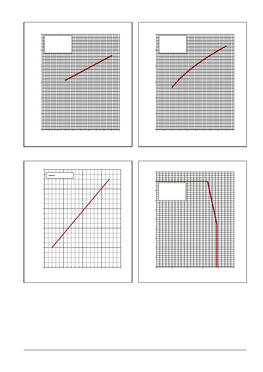
GCT Part
0
200
400
600
800
1000
1.5
2.0
2.5
3.0
3.5
4.0
V
T
[V]
I
T
[A]
Tj = 115�C
0
100 200 300 400 500 600 700 800 900 1000
I
TGQ
[A]
0.0
0.5
1.0
1.5
2.0
2.5
3.0
3.5
4.0
4.5
5.0
E
off
[J]
T
j
= 115�C
V
D
= 3300 V
Fig. 1
GCT on-state characteristics.
Fig. 2
GCT turn-off energy per pulse vs.
turn-off current.
0
100
200
300
400
500
600
700
800
900
1000
0
1000
2000
3000
4000
5000
V
D
[V]
I
TGQ
[A]
T
j
= 0..115 �C
V
DM
V
DRM
L
i
= 11.5
�
�
�
�H
C
CL
= 2.0
�
�
�
�F
L
CL
= 0.6
�
�
�
�H
R
s
= 1.25
Fig. 3
Max. repetitive GCT turn-off current.
5SHX 10H6004
ABB Switzerland Ltd, Semiconductors reserves the right to change specifications without notice.
Doc. No. 5SYA1226-03 Jan. 02
page 6 of 9
Diode Part
0
100 200 300 400 500 600 700 800 900 1000
I
FQ
[A]
200
250
300
350
400
450
500
I
rr
[A]
T
j
= 115�C
di
F
/dt = 290 A/�s
V
D
= 3300 V
0
100 200 300 400 500 600 700 800 900 1000
I
FQ
[A]
0.0
0.5
1.0
1.5
2.0
2.5
3.0
E
rr
[J]
T
j
= 115�C
di
F
/dt = 290 A/�s
V
D
= 3300 V
Fig. 4
Diode reverse recovery current vs.
turn-off current.
Fig. 5
Diode turn-off energy per pulse vs.
turn-off current.
0
200
400
600
800
1000
3.0
4.0
5.0
6.0
7.0
V
F
[V]
I
F
[A]
Tj = 115�C
0
1000
2000
3000
4000
5000
V
D
[V]
0
100
200
300
400
500
600
700
800
900
1000
I
FQ
[A]
T
j
= 0 - 115�C
di
F
/dt = 290 A/�s
V
DM
V
DRM
Fig. 6
Diode on-state characteristics.
Fig. 7
Max. repetitive diode forward
current.

5SHX 10H6004
ABB Switzerland Ltd, Semiconductors reserves the right to change specifications without notice.
Doc. No. 5SYA1226-03 Jan. 02
page 7 of 9
0
50
100
150
200
250
300
350
400
I
TGQ ave
[A]
0
5
10
15
20
25
30
35
40
45
50
P
Gin
[W]
fs = 1000 Hz
fs = 500 Hz
fs = 50 Hz
Fig. 8
Gate Unit power consumption.
Fig. 9
Device Outline Drawing.

5SHX 10H6004
ABB Switzerland Ltd, Semiconductors reserves the right to change specifications without notice.
Doc. No. 5SYA1226-03 Jan. 02
page 8 of 9
RC-IGCT
Logic
Monitoring
Turn-
Off
Circuit
Turn-
On
Circuit
Gate
Cathode
Internal Supply (without galvanic isolation to power circuit)
Supply (20V
DC
)
X
1
CS
Rx
Command Signal (Light)
Anode
Gate Unit
RC-GCT
Fig. 10
Block diagram.

5SHX 10H6004
ABB Switzerland Ltd, Semiconductors reserves the right to change specifications without notice.
ABB Switzerland Ltd
Doc. No. 5SYA1226-03 Jan. 02
Semiconductors
Fabrikstrasse 3
CH-5600 Lenzburg, Switzerland
Telephone +41 (0)58 586 1419
Fax
+41 (0)58 586 1306
Email
abbsem@ch.abb.com
Internet
www.abbsem.com
1
CS
CS
I
T
V
DSP
V
DM
V
D
0.3 I
TGQ
0.8 I
TGQ
0.05 V
D
V
G
t
don
t
f
t
r
t
doff
I
T
I
TM
di/dt
0.9 V
D
0.1 V
D
V
D
Turn-on
Turn-off
V
G
Fig. 11
General current and voltage waveforms with IGCT-specific symbols.
L
CL
L
i
R
s
DUT
GCT - part
L
Load
DUT
Diode - part
C
CL
V
LC
Fig. 12
Test circuit.