
1)
Maximum Ratings are those values beyond which damage to the device may occur
ABB Switzerland Ltd, Semiconductors reserves the right to change specifications without notice.
V
DSM
=
2800 V
I
TAVM
=
620 A
I
TRMS
=
970 A
I
TSM
=
8000 A
V
T0
=
0.92 V
r
T
=
0.78 m
Phase Control Thyristor
5STP 06D2800
Doc. No. 5SYA1020-04 Jan. 02
∑
∑
∑
∑ Patented free-floating silicon technology
∑
∑
∑
∑ Low on-state and switching losses
∑
∑
∑
∑ Designed for traction, energy and industrial applications
∑
∑
∑
∑ Optimum power handling capability
Blocking
Maximum rated values
1)
Symbol
Conditions
5STP 06D2800 5STP 06D2600 5STP 06D2200
V
DRM,
V
RRM
f = 50 Hz, t
p
= 10ms
2800 V
2600 V
2200 V
V
RSM1
t
p
= 5ms, single pulse
3000 V
2800 V
2400 V
dV/dt
crit
Exp. to 0.67 x V
DRM
, T
j
= 125∞C
1000 V/µs
Characteristic values
Parameter
Symbol Conditions
min
typ
max
Unit
Forwarde leakage current
I
DRM
V
DRM
, Tj = 125∞C
100
mA
Reverse leakage current
I
RRM
V
RRM
, Tj = 125∞C
100
mA
Mechanical data
Maximum rated values
1)
Parameter
Symbol Conditions
min
typ
max
Unit
Mounting force
F
M
8
10
12
kN
Acceleration
a
Device unclamped
50
m/s
2
Acceleration
a
Device clamped
100
m/s
2
Characteristic values
Parameter
Symbol Conditions
min
typ
max
Unit
Weight
m
0.3
kg
Surface creepage distance
D
S
25
mm
Air strike distance
D
a
14
mm

5STP 06D2800
ABB Switzerland Ltd, Semiconductors reserves the right to change specifications without notice.
Doc. No. 5SYA1020-04 Jan. 02
page 2 of 6
On-state
Maximum rated values
1)
Parameter
Symbol Conditions
min
typ
max
Unit
Max. average on-state
current
I
TAVM
Half sine wave, T
c
= 70∞C
620
A
RMS on-state current
I
TRMS
970
A
Max. peak non-repetitive
surge current
I
TSM
8000
A
Limiting load integral
I
2
t
tp = 10 ms, Tj = 125∞C,
V
D
=V
R
= 0 V
320
kA
2
s
Max. peak non-repetitive
surge current
I
TSM
8500
A
Limiting load integral
I
2
t
tp = 8.3 ms, Tj = 125∞C,
V
D
=V
R
=0 V
300
kA
2
s
Characteristic values
Parameter
Symbol Conditions
min
typ
max
Unit
On-state voltage
V
T
I
T
= 1000 A, T
j
= 125∞C
1.7
V
Threshold voltage
V
T0
I
T
= 333 A - 1000 A, T
j
= 125∞C
0.92
V
Slope resistance
r
T
Tj = 125∞C
0.78
m
Holding current
I
H
T
j
= 25∞C
70
mA
T
j
= 125∞C
50
mA
Latching current
I
L
T
j
= 25∞C
500
mA
T
j
= 125∞C
200
mA
Switching
Maximum rated values
1)
Parameter
Symbol Conditions
min
typ
max
Unit
Critical rate of rise of on-
state current
di/dt
crit
Cont.
f = 50 Hz
150
A/µs
Critical rate of rise of on-
state current
di/dt
crit
T
j
= 125∞C, I
TRM
= 1500 A,
V
D
0.67V
DRM
,
I
FG
= 2 A, t
r
= 0.5 µs
Cont.
f = 1Hz
1000
A/µs
Circuit-commutated turn-off
time
t
q
T
j
= 125∞C, I
TRM
= 1500 A,
V
R
= 200 V, di
T
/dt = -20 A/µs,
V
D
0.67V
DRM
, dv
D
/dt = 20 V/µs,
400
µs
Characteristic values
Parameter
Symbol Conditions
min
typ
max
Unit
Recovery charge
Q
rr
T
j
= 125∞C, I
TRM
= 1500 A,
V
R
= 200 V, di
T
/dt = -20 A/µs
1500
3200
µAs
Delay time
t
d
V
D
= 0.4
V
DRM
, I
FG
= 2 A, t
r
= 0.5 µs
3
µs

5STP 06D2800
ABB Switzerland Ltd, Semiconductors reserves the right to change specifications without notice.
Doc. No. 5SYA1020-04 Jan. 02
page 3 of 6
Triggering
Maximum rated values
1)
Parameter
Symbol Conditions
min
typ
max
Unit
Peak forward gate voltage
V
FGM
12
V
Peak forward gate current
I
FGM
10
A
Peak reverse gate voltage
V
RGM
10
V
Gate power loss
P
G
For DC gate current
3
W
Average gate power loss
P
GAV
see Fig. 9
Characteristic values
Parameter
Symbol Conditions
min
typ
max
Unit
Gate trigger voltage
V
GT
T
j
= 25∞C
2.6
V
Gate trigger current
I
GT
T
j
= 25∞C
400
mA
Gate non-trigger voltage
V
GD
V
D
= 0.4 x V
DRM
, T
vjmax
= 125∞C
0.3
V
Gate non-trigger current
I
GD
V
D
= 0.4 x V
DRM
, T
vjmax
= 125∞C
10
mA
Thermal
Maximum rated values
1)
Parameter
Symbol Conditions
min
typ
max
Unit
Operating junction
temperature range
T
j
125
∞C
Storage temperature range T
stg
-40
140
∞C
Characteristic values
Parameter
Symbol Conditions
min
typ
max
Unit
Thermal resistance junction
to case
R
th(j-c)
Double side cooled
36
K/kW
R
th(j-c)A
Anode side cooled
70
K/kW
R
th(j-c)C
Cathode side cooled
74
K/kW
Thermal resistance case to
heatsink
R
th(c-h)
Double side cooled
7.5
K/kW
R
th(c-h)
Single side cooled
15
K/kW
Analytical function for transient thermal
impedance:
)
e
-
(1
R
=
(t)
Z
n
1
i
t/
-
i
thJC
i
Â
=
i
1
2
3
4
R
i
(K/kW)
19.18
9.82
5.45
1.44
i
(s)
0.3862
0.0561
0.0058
0.0024
Fig. 1 Transient thermal impedance junction-to case.
5STP 06D2800
ABB Switzerland Ltd, Semiconductors reserves the right to change specifications without notice.
Doc. No. 5SYA1020-04 Jan. 02
page 4 of 6
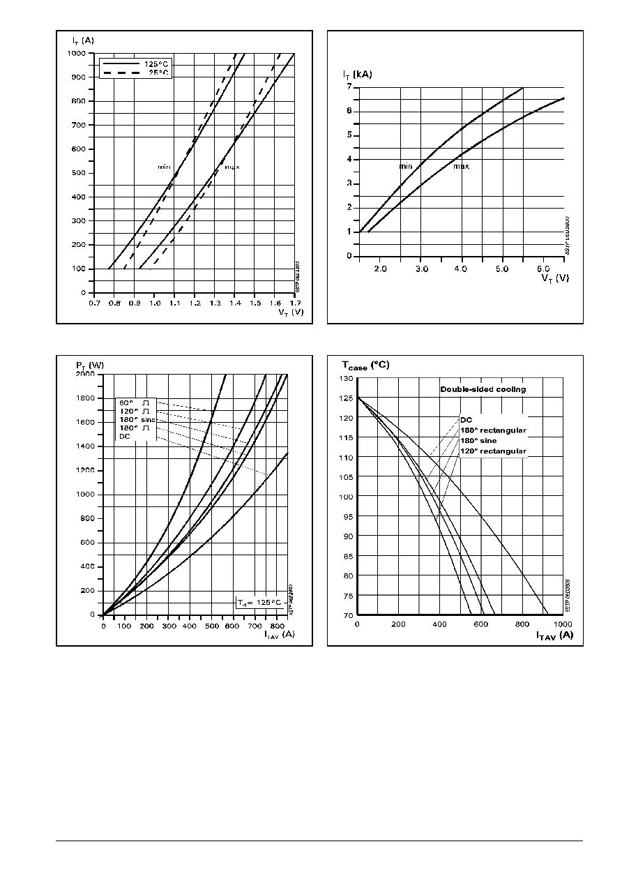
Fig. 2 On-state characteristics.
Fig. 3 On-state characteristics.
T
j
=125∞C, 10ms half sine
Fig. 4 On-state power dissipation vs. mean on-
state current. Turn - on losses excluded.
Fig. 5 Max. permissible case temperature vs.
mean on-state current.
5STP 06D2800
ABB Switzerland Ltd, Semiconductors reserves the right to change specifications without notice.
Doc. No. 5SYA1020-04 Jan. 02
page 5 of 6
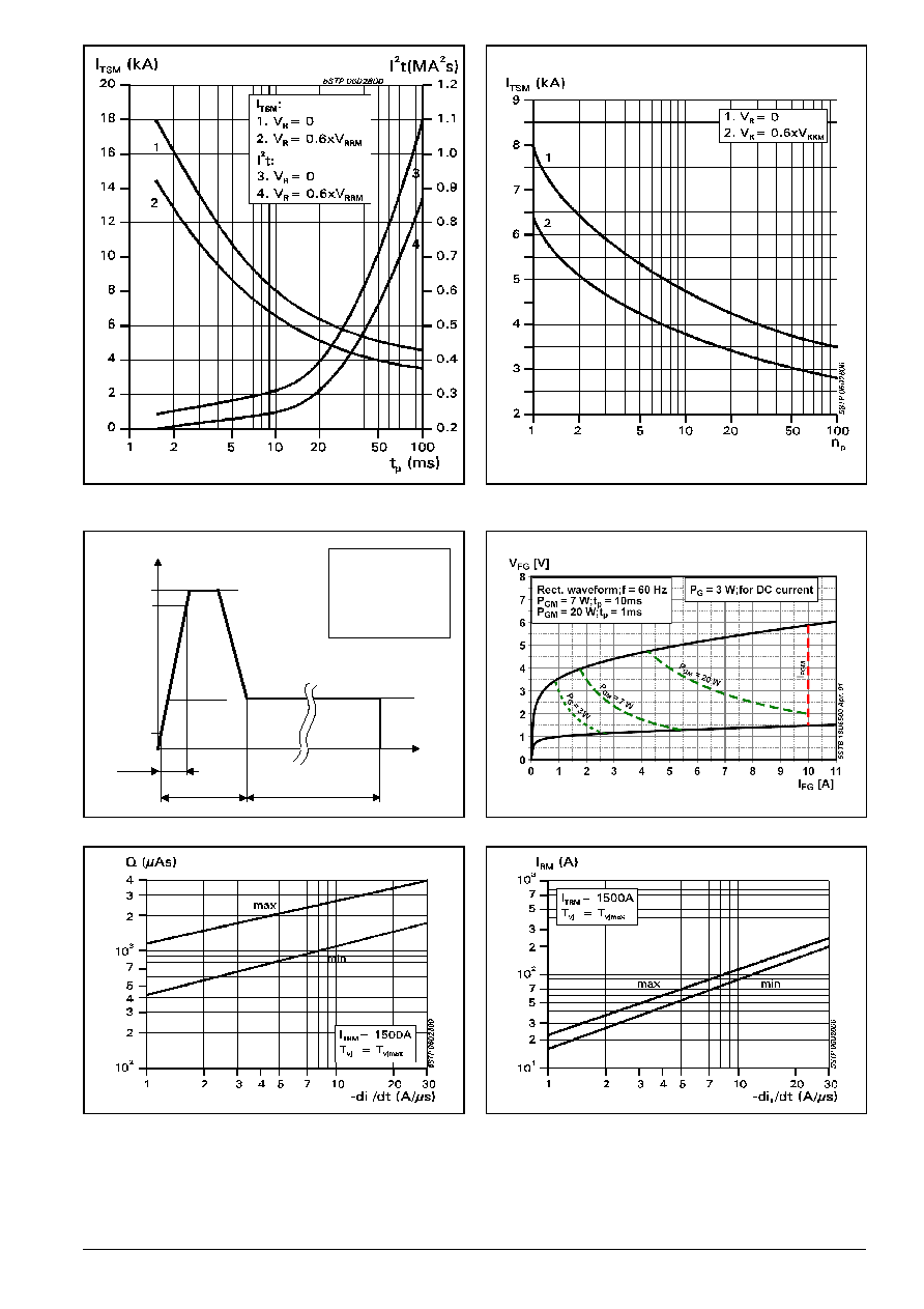
Fig. 6 Surge on-state current vs. pulse length. Half-
sine wave.
Fig. 7 Surge on-state current vs. number of pulses.
Half-sine wave, 10 ms, 50Hz.
I
GM
I
Gon
100 %
90 %
10 %
I
GM
2..5 A
I
Gon
1.5 I
GT
di
G
/dt
2 A/µs
t
r
1 µs
t
p
(I
GM
)
5...20µs
di
G
/dt
t
r
t
p
(I
GM
)
I
G
(t)
t
t
p
(I
Gon
)
Fig. 8 Recommendet gate current waveform.
Fig. 9 Max. peak gate power loss.
Fig. 10 Recovery charge vs. decay rate of on-state
current.
Fig. 11 Peak reverse recovery current vs. decay rate
of on-state current.

5STP 06D2800
ABB Switzerland Ltd, Semiconductors reserves the right to change specifications without notice.
ABB Switzerland Ltd
Doc. No. 5SYA1020-04 Jan. 02
Semiconductors
Fabrikstrasse 3
CH-5600 Lenzburg, Switzerland
Telephone +41 (0)58 586 1419
Fax
+41 (0)58 586 1306
Email
abbsem@ch.abb.com
Internet
www.abbsem.com
Fig. 12 Device Outline Drawing.