3.3 Vdc ∑ HCMOS/TTL ∑ J -LEADED ∑ PLASTIC MOLDED ∑ SURFACE MOUNT
CRYSTAL CLOCK OSCILLATORS
ASML
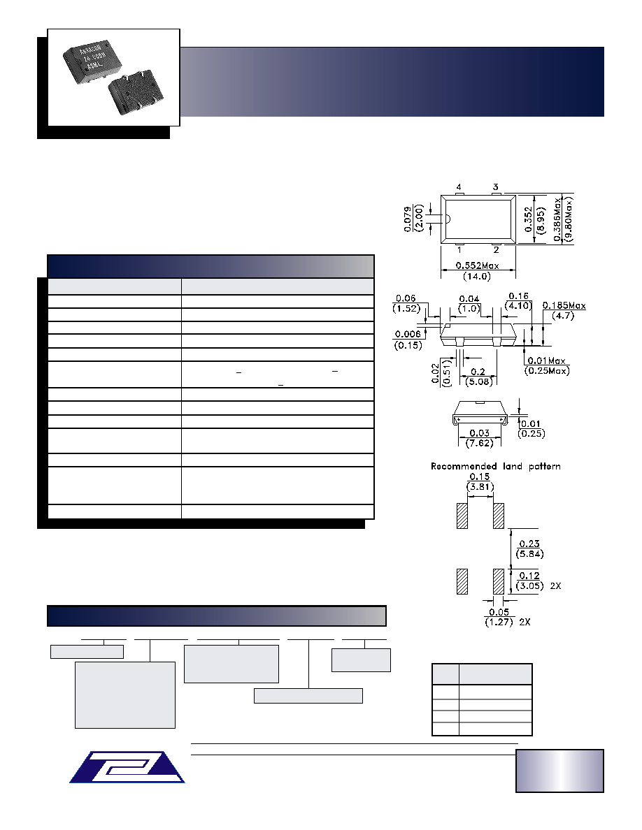
Dimensions: Inches (mm)
APPLICATIONS:
∑ Provide clock signals for microprocessors and digital circuits.
∑ Communication equipment, AV and OA equipment
FEATURES:
∑ Industry standard J-Leaded terminals.
∑ Plastic molded SMD, Reflow capable.
∑ Low current consumption.
∑ Tristate Enable / Disable.
∑ HCMOS output.
∑ 3.3Vdc operation.
∑ Extended temperature -40∞C to +85∞C option.
Frequency Range
3.5 MHz - 25 MHz
Operation Mode
Fundamental, AT
Operating Temperature
-10∞C to + 60∞ C
(See Options)
Storage Temperature
-55∞C to + 125∞ C
Frequency Tolerance
@
25∞C
±50 ppm max.
(See Options)
Frequency Stability over Temp.
±50 ppm max.
(See Options)
Equivalent Series Resistance
200 W for 3.5 MHz < F < 4.0 MHz
(ESR) Maximum
150 W for 4.0 MHz < F < 6.0 MHz
100 W for 6.0 MHz < F < 10.0 MHz
80 W for 10 MHz < F < 14.0 MHz
50 W for 14 MHz < F <_ 25 MHz
Shunt Capacitance C
0
7 pF max.
Load Capacitance C
L
16pF
(See Option)
Drive Level
100µW max.
Aging
@
25∞ C First Year
± 5 ppm max.
Insulation Resistance
500
M
W
min. at 100 Vdc ± 15V
PARAMETERS
SPECIFICATIONS
STANDARD
SPECIFICATIONS
Frequency Range (F
o
)
1MHz - 160MHz
Operating Temperature (T
OPR
)
0∞C to +70∞C
(See Options)
Storage Temperature
(T
STO
)
- 40∞C to +85∞C
Frequency Stability (DF/ F
o
)
±100ppm max.
(See Options)
Supply Voltage
(V
dd
)
3.3Vdc ±10%
Input Current (I
dd
)
10mA max. (F < 20MHz
) ;
25mA max. (F < 70MHz)
60mA max. (F < 160MHz)
Duty Cycle or Symmetry
40 / 60% max.
(See Options)
Rise and Fall Times (T
R
/
T
F
)
6ns max.
Output Load
2TTL, 15pF max.
Output Voltage
(V
OH
)
0.9 *Vdd min.
(V
OL
)
0.4Vdc max.
Start-up Time
(T
OSC
)
10ms max.
Tristate Function
(V
IH
)
(V
IL
)
Aging ±5ppm/ Year max.
AS ML - Frequency - Temperature - Frequency Stability - Duty Cycle - Packaging
XX.XXXXX MHz
-R for ± 25ppm max
-K for ± 30ppm max
-C for ± 50ppm max
-S for 45 /55%
@
1
/
2Vdd
-T
(Tape & Reel)
-D for -10∞C to + 60∞C
-E for -20∞C to + 70∞C
-F for -30∞C to + 70∞C
-N for -30∞C to + 85∞C
-L for -40∞C to + 85∞C
ORDERING
OPTIONS
PIN
FUNCTION
N0.
1 Tristate Enable
2 GND / Case
3 Output
4 Vdd
"1" or Open: Oscillation
>
_ 2.2V
"0": (HiZ)
< 0.6V
Output disabled in high impedance
* Pin 1 has internal pull-up resistor which allows Pin 1 to be left floating (enable high)
Test circuit, waveform, please see appendix B.
Environmental and mechanical specifications, see appendix C. Group 2.
Marking, see appendix G. Tape and Reel, see appendix H.(1,000 pcs./reel).
A bypass capacitor 0.01 µF is required from Vdd to Gnd.
Application notes, see appendix A. Reflow profile, see appendix E.
14.0 x 8.95 x 4.7 mm
ABRACON IS
ISO 9001 / QS 9000
CERTIFIED
NOTE: Left blank if standard
∑ All specifications and markings subject to change without notice
29 Journey ∑ Aliso Viejo, CA 92656 ∑ USA
(949) 448-7070 ∑ F
AX
: (949) 448-8484
E-
MAIL
:
abinfo
@
abracon.com ∑
I
NTERNET
A
DDRESS
:
www.abracon.com
ABRACON IS
ISO 9001 / QS 9000
CERTIFIED
ABRACON
Æ
C O R P O R A T I O N
48