 | –≠–ª–µ–∫—Ç—Ä–æ–Ω–Ω—ã–π –∫–æ–º–ø–æ–Ω–µ–Ω—Ç: A40MX02-M | –°–∫–∞—á–∞—Ç—å:  PDF PDF  ZIP ZIP |
F e b r u a r y 2 0 0 1
1
© 2001 Actel Corporation
5 . 0
40MX and 42MX FPGA Families
F e a t u r e s
H i g h C a p a c i t y
∑ Single-Chip ASIC Alternative
∑ 3,000 to 54,000 System Gates
∑ Up to 2.5 kbits Configurable Dual-Port SRAM
∑ Fast Wide-Decode Circuitry
∑ Up to 202 User-Programmable I/O Pins
H i g h P e r f o r m a n c e
∑ 5.6 ns Clock-to-Out
∑ 250 MHz Performance
∑ 5 ns Dual-Port SRAM Access
∑ 100 MHz FIFOs
∑ 7.5 ns 35-Bit Address Decode
H i R e l F e a t u r e s
∑ Commercial, Industrial, and Military Temperature Plastic
Packages
∑ Commercial, Military Temperature and MIL-STD-883
Ceramic Packages
∑ QML Certification
∑ Ceramic Devices Available to DSCC SMD
E a s e o f I n t e g r a t i o n
∑ Mixed Voltage Operation (5.0V or 3.3V I/O)
∑ Synthesis-Friendly Architecture to Support ASIC Design
Methodologies
∑ Up to 100% Resource Utilization and 100% Pin Fixing
∑ Deterministic, User-Controllable Timing
∑ Unique In-System Diagnostic and Verification Capability
with Silicon Explorer II
∑ Low Power Consumption
∑ IEEE Standard 1149.1 (JTAG) Boundary Scan Testing
∑ 5.0V and 3.3V Programmable PCI-Compliant I/O
P r o d u c t P r o f i l e
Device
A40MX02
A40MX04
A42MX09
A42MX16
A42MX24
A42MX36
Capacity
System Gates
SRAM Bits
3,000
N/A
6,000
N/A
14,000
N/A
24,000
N/A
36,000
N/A
54,000
2,560
Logic Modules
Sequential
Combinatorial
Decode
--
295
--
--
547
--
348
336
N/A
624
608
N/A
954
912
24
1,230
1,184
24
Clock-to-Out
9.5 ns
9.5 ns
5.6 ns
6.1 ns
6.1 ns
6.3 ns
SRAM Modules
(64x4 or 32x8)
N/A
N/A
N/A
N/A
N/A
10
Dedicated Flip-Flops
--
--
348
624
954
1,230
Maximum Flip-Flops
147
273
516
928
1,410
1,822
Clocks
1
1
2
2
2
6
User I/O
(Maximum)
57
69
104
140
176
202
PCI
No
No
No
No
Yes
Yes
Boundary Scan Test (BST)
No
No
No
No
Yes
Yes
Packages (by pin count)
PLCC
PQFP
VQFP
TQFP
CQFP
PBGA
44, 68
100
80
--
--
--
44, 68, 84
100
80
--
--
--
84
100, 160
100
176
--
--
84
100, 160, 208
100
176
--
--
84
160, 208
--
176
--
--
--
208, 240
--
--
208, 256
272
v 5 . 0
4 0 M X a n d 4 2 M X F P G A F a m i l i e s
2
v5.0
G e n e r a l D e s c r i p t i o n
Actel's 40MX and 42MX families provide a
high-performance, single-chip solution for shortening the
system design and development cycle, offering a
cost-effective alternative to ASICs. The 40MX and 42MX
devices are excellent choices for integrating logic that is
currently implemented in multiple PALs, CPLDs, and
FPGAs. Example applications include high-speed
controllers and address decoding, peripheral bus interfaces,
DSP, and co-processor functions.
The MX device architecture is based on Actel's patented
antifuse technology implemented in a 0.45µ triple-metal
CMOS process. With capacities ranging from 3,000 to 54,000
system gates, the synthesis-friendly MX devices provide
performance up to 250 MHz, are live on power-up, and
require up to five times lower stand-by power consumption
than any other FPGA device. Actel's MX FPGAs provide up
to 202 user I/Os and are available in a wide variety of
packages and speed grades.
Actel's 42MX devices also feature MultiPlex I/Os, which
support mixed voltage systems, enable programmable PCI,
deliver high-performance operation at both 5.0V and 3.3V,
and provide a low-power mode.
The MX PCI-Compliant devices are fully compliant with the
PCI Local Bus Specification (version 2.1). They deliver 200
MHz on-chip operation and 6.1 ns clock-to-output
performance with capacities spanning from 36,000 to 54,000
system gates. MX devices comply 100 percent to the
electrical and timing specifications detailed in the PCI
specification. However, as with all programmable logic
devices, the performance of the final product depends upon
the user's design and optimization techniques.
The MX24 and MX36 devices also include system-level
features such as IEEE Standard 1149.1 (JTAG) Boudary
Scan Testing, dual-port SRAM, and fast wide-decode
modules. The A42MX36 device offers dual-port SRAM for
implementing fast FIFOs, LIFOs, and temporary data
storage. The large number of storage elements can
efficiently address applications requiring wide datapath
manipulation and can perform transformation functions
such as those required for telecommunications, networking,
and DSP.
All products in the 40MX and 42MX families are available
100 percent tested over the military temperature range. In
addition, the largest member of the family, the A42MX36, is
available in both CQ208 and CQ256 ceramic packages
screened to MIL-STD-883 levels. For easy prototyping and
conversion from plastic to ceramic, the CQ208 and PQ208
devices are pin compatible.
O r d e r i n g I n f o r m a t i o n
Application (Temperature Range)
Blank = Commercial (0 to +70∞C)
I = Industrial (≠40 to +85∞C)
M = Military (≠55 to +125∞C)
B = MIL-STD-883
Package Type
PL = Plastic Leaded Chip Carrier
PQ = Plastic Quad Flat Pack
TQ = Thin (1.4 mm) Quad Flat Pack
VQ = Very Thin (1.0 mm) Quad Flat Pack
BG = Ball Grid Array
CQ = Ceramic Quad Flat Pack
Speed Grade
Blank = Standard Speed
≠1 = Approximately 15% Faster than Standard
≠2 = Approximately 25% Faster than Standard
≠3 = Approximately 35% Faster than Standard
≠F = Approximately 40% Slower than Standard
Part Number
A40MX02= 3,000 System Gates
A40MX04= 6,000 System Gates
A42MX09= 14,000 System Gates
A42MX16= 24,000 System Gates
A42MX24= 36,000 System Gates
A42MX36= 54,000 System Gates
Package Lead Count
A42MX16
≠
PQ
100

v5.0
3
4 0 M X a n d 4 2 M X F P G A F a m i l i e s
P r o d u c t P l a n
Speed Grade
*
Application
Std
≠1
≠2
≠3
≠F
C
I
M
B
A40MX02 Device
44-Pin Plastic Leaded Chip Carrier (PLCC)
--
68-Pin Plastic Leaded Chip Carrier (PLCC)
--
100-Pin Plastic Quad Flat Pack (PQFP)
--
80-Pin Very Thin Plastic Quad Flat Pack (VQFP)
--
A40MX04 Device
44-Pin Plastic Leaded Chip Carrier (PLCC)
--
68-Pin Plastic Leaded Chip Carrier (PLCC)
--
84-Pin Plastic Leaded Chip Carrier (PLCC)
--
100-Pin Plastic Quad Flat Pack (PQFP)
--
80-Pin Very Thin Plastic Quad Flat Pack (VQFP)
--
A42MX09 Device
84-Pin Plastic Leaded Chip Carrier (PLCC)
--
100-Pin Plastic Quad Flat Pack (PQFP)
--
160-Pin Plastic Quad Flat Pack (PQFP)
--
176-Pin Thin Plastic Quad Flat Pack (TQFP)
--
100-Pin Very Thin Plastic Quad Flat Pack (VQFP)
--
A42MX16 Device
84-Pin Plastic Leaded Chip Carrier (PLCC)
--
100-Pin Plastic Quad Flat Pack (PQFP)
--
160-Pin Plastic Quad Flat Pack (PQFP)
--
208-Pin Plastic Quad Flat Pack (PQFP)
--
176-Pin Thin Plastic Quad Flat Pack (TQFP)
--
100-Pin Very Thin Plastic Quad Flat Pack (VQFP)
--
A42MX24 Device
84-Pin Plastic Leaded Chip Carrier (PLCC)
--
160-Pin Plastic Quad Flat Pack (PQFP)
--
208-Pin Plastic Quad Flat Pack (PQFP)
--
176-Pin Thin Plastic Quad Flat Pack (TQFP)
--
A42MX36 Device
208-Pin Plastic Quad Flat Pack (PQFP)
--
240-Pin Plastic Quad Flat Pack (PQFP)
--
272-Pin Plastic Ball Grid Array (PBGA)
--
208-Pin Ceramic Quad Flat Pack (CQFP)
--
--
--
∑
∑
256-Pin Ceramic Quad Flat Pack (CQFP)
--
--
--
∑
∑
Contact your Actel sales representative for product availability.
Applications:
C
= Commercial
Availability:
= Available
*Speed Grade:
≠1 = Approx. 15% faster than Standard
I
= Industrial
P
= Planned
≠2 = Approx. 25% faster than Standard
M
= Military
-- = Not Planned
≠3 = Approx. 35% faster than Standard
≠F = Approx. 40% slower than Standard
Only Std, ≠1, ≠2 Speed Grade
∑
Only Std, ≠1 Speed Grade

4 0 M X a n d 4 2 M X F P G A F a m i l i e s
4
v5.0
D e v e l o p m e n t T o o l S u p p o r t
The MX devices are fully supported by Actel's line of FPGA
development tools, including the Actel DeskTOP series and
Designer Series tools. The Actel DeskTOP series is an
integrated design environment for PCs that includes design
entry, simulation, synthesis, and place-and-route tools.
Designer Series, Actel's suite of FPGA development point
tools for PCs and Workstations, includes the ACTgen Macro
Builder, timing-driven place-and-route and analysis tools,
and device programming software.
In addition, the MX devices contain ActionProbe circuitry
that provides built-in access to every node in a design,
enabling 100 percent real-time observation and analysis of a
device's internal logic nodes without design iteration. The
probe circuitry is accessed by Silicon Explorer II, an
easy-to-use integrated verification and logic analysis tool
that can sample data at 100 MHz (asynchronous) or 66 MHz
(synchronous). Silicon Explorer II attaches to a PC's
standard COM port, turning the PC into a fully functional
18-channel logic analyzer. Silicon Explorer II allows
designers to complete the design verification process at
their desks and reduces verification time from several hours
per cycle to only a few seconds.
P l a s t i c D e v i c e R e s o u r c e s
User I/Os
Device
PLCC
44-Pin
PLCC
68-Pin
PLCC
84-Pin
PQFP
100-Pin
PQFP
160-Pin
PQFP
208-Pin
PQFP
240-Pin
VQFP
80-Pin
VQFP
100-Pin
TQFP
176-Pin
PBGA
272-Pin
A40MX02
34
57
--
57
--
--
--
57
--
--
--
A40MX04
34
57
69
69
--
--
--
69
--
--
--
A42MX09
--
--
72
83
101
--
--
--
83
104
--
A42MX16
--
--
72
83
125
140
--
--
83
140
--
A42MX24
--
--
72
--
125
176
--
--
--
150
--
A42MX36
--
--
--
--
--
176
202
--
--
--
202
Package Definitions (Contact your Actel sales representative for product availability.)
PLCC = Plastic Leaded Chip Carrier, PQFP = Plastic Quad Flat Pack, TQFP = Thin Quad Flat Pack, VQFP = Very Thin Quad Flat Pack,
PBGA = Plastic Ball Grid Array
C e r a m i c D e v i c e R e s o u r c e s
User I/Os
Device
CQFP
208-Pin
CQFP
256-Pin
A42MX36
176
202
Package Definitions (Contact your Actel sales representative for product availability.)
CQFP = Ceramic Quad Flat Pack

v5.0
5
4 0 M X a n d 4 2 M X F P G A F a m i l i e s
P o w e r R e q u i r e m e n t s
4 0 M X
The 40MX FPGAs will operate in 5.0V-only systems or
3.3V-only systems.
V
CC
Input
Output
5.0V
5.0V
5.0V
3.3V
3.3V
3.3V
4 2 M X
The 42MX FPGAs will operate in 5.0V-only systems,
3.3V-only systems, or mixed 5.0V/3.3V systems.
V
CCA
V
CCI
Input
Output
5.0V
5.0V
5.0V
5.0V
3.3V
3.3V
3.3V
3.3V
5.0V
3.3V
3.3V, 5.0V
3.3V
M i x e d V o l t a g e P o w e r U p a n d P o w e r
D o w n
When powering up the device in the mixed voltage mode
(V
CCA
= 5.0V and V
CCI
= 3.3V), V
CCA
must be greater than or
equal to V
CCI
throughout the power-up sequence. If V
CCI
is
0.5V greater than V
CCA
when both are above 1.5V, then the
I/Os' input protection junction on the I/Os will be forward
biased, causing them to draw large amounts of current.
When V
CCA
and V
CCI
are in the 1.5V to 2.0V region and V
CCI
is greater than V
CCA
, all I/Os would momentarily behave as
outputs that are in a logical high state, and I
CC
rises to high
levels. For power down, any sequence with V
CCA
and V
CCI
can be implemented.
L o w P o w e r M o d e
The 42MX devices have a power-saving feature enabled by a
special Low Power pin (LP). In this mode, the device
consumes very minimal power, with standby current as low
as 15µA (see
"Electrical Specifications" on page 13
and
14
).
All µ I/Os are tristated, all input buffers are turned off, and
the core of the device is turned off. Since the core is turned
off, the state of the registers and the contents of the SRAM
are lost. The device enters low power mode 800ns after the
LP pin is set High. It will resume normal operation 200µs
after the LP pin is driven to a logic Low.
M X A r c h i t e c t u r a l O v e r v i e w
The 40MX and 42MX devices are composed of fine-grained
building blocks that enable fast, efficient logic designs. All
devices within these families are composed of logic
modules, I/O modules, routing resources, and clock
networks, which are the building blocks for designing fast
logic designs. In addition, the A42MX36 device contains
embedded dual-port SRAM and wide decode modules. The
dual-port SRAM modules are optimized for high-speed
datapath functions such as FIFOs, LIFOs, and scratchpad
memory. The
"Product Profile" on page 1
lists the specific
logic resources contained within each device.
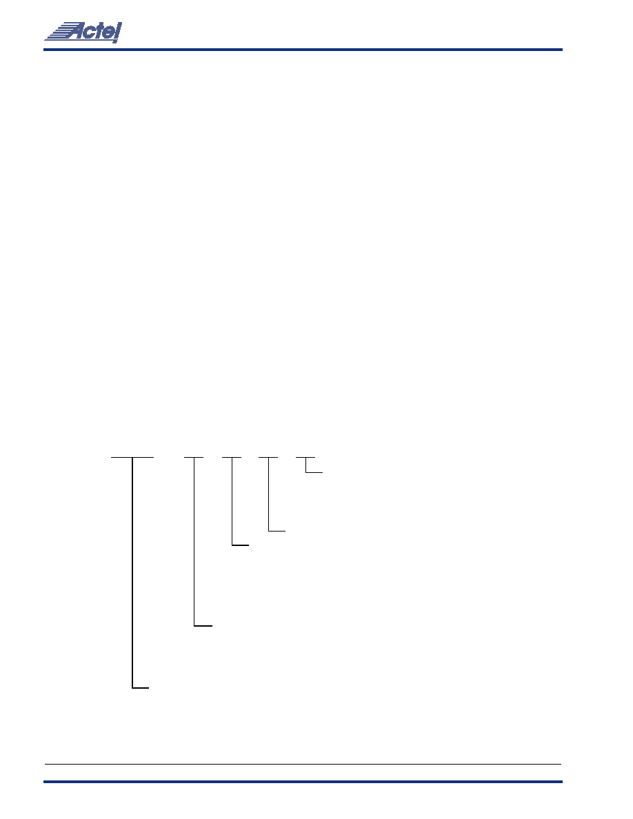
L o g i c M o d u l e s
The 40MX logic module is an eight-input, one-output logic
circuit designed to implement a wide range of logic
functions with efficient use of interconnect routing
resources (
Figure 1
).
The logic module can implement the four basic logic
functions (NAND, AND, OR, and NOR) in gates of two, three,
or four inputs. Each function may have many versions with
different combinations of active LOW inputs. The logic
module can also implement a variety of D-latches,
exclusivity functions, AND-ORs, and OR-ANDs. No dedicated
hard-wired latches or flip-flops are required in the array,
since latches and flip-flops can be constructed from logic
modules wherever needed in the application.
Figure 1 ∑ 40MX Logic Module