REV. D
Information furnished by Analog Devices is believed to be accurate and
reliable. However, no responsibility is assumed by Analog Devices for its
use, nor for any infringements of patents or other rights of third parties
which may result from its use. No license is granted by implication or
otherwise under any patent or patent rights of Analog Devices.
a
AMP01*
Low Noise, Precision
Instrumentation Amplifier
GENERAL DESCRIPTION
The AMP01 is a monolithic instrumentation amplifier designed
for high-precision data acquisition and instrumentation applica-
tions. The design combines the conventional features of an
instrumentation amplifier with a high current output stage. The
output remains stable with high capacitance loads (1
µ
F), a
unique ability for an instrumentation amplifier. Consequently,
the AMP01 can amplify low level signals for transmission
through long cables without requiring an output buffer. The output
stage may be configured as a voltage or current generator.
Input offset voltage is very low (20
µ
V), which generally elimi-
nates the external null potentiometer. Temperature changes
have minimal effect on offset; TCV
IOS
is typically 0.15
µ
V/
∞
C.
Excellent low-frequency noise performance is achieved with a
minimal compromise on input protection. Bias current is very
low, less than 10 nA over the military temperature range. High
common-mode rejection of 130 dB, 16-bit linearity at a gain of
1000, and 50 mA peak output current are achievable simulta-
neously. This combination takes the instrumentation amplifier
one step further towards the ideal amplifier.
AC performance complements the superb dc specifications. The
AMP01 slews at 4.5 V/
µ
s into capacitive loads of up to 15 nF,
settles in 50
µ
s to 0.01% at a gain of 1000, and boasts a healthy
26 MHz gain-bandwidth product. These features make the
AMP01 ideal for high speed data acquisition systems.
Gain is set by the ratio of two external resistors over a range of
0.1 to 10,000. A very low gain temperature coefficient of
10 ppm/
∞
C is achievable over the whole gain range. Output
voltage swing is guaranteed with three load resistances; 50
,
500
, and 2 k
. Loaded with 500
, the output delivers
±
13.0 V minimum. A thermal shutdown circuit prevents de-
struction of the output transistors during overload conditions.
The AMP01 can also be configured as a high performance op-
erational amplifier. In many applications, the AMP01 can be
used in place of op amp/power-buffer combinations.
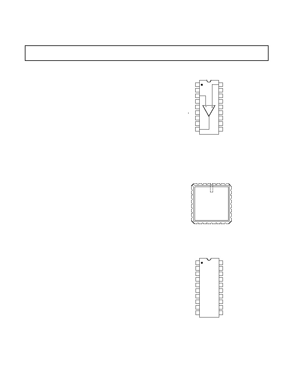
PIN CONFIGURATIONS
18-Lead Cerdip
TOP VIEW
(Not to Scale)
18
17
16
15
14
13
12
11
10
1
2
3
4
5
6
7
8
9
AMP01
OUTPUT
REFERENCE
R
G
R
G
≠IN
V
OOS
NULL
SENSE
TEST PIN*
V
OOS
NULL
≠V
OP
V≠
+IN
V
IOS
NULL
V
IOS
NULL
R
S
V+
+V
OP
R
S
*MAKE NO ELECTRICAL CONNECTION
AMP01 BTC/883
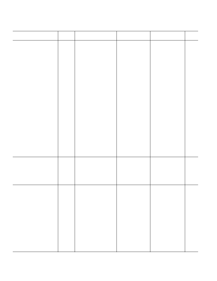
28-Terminal LCC
NC = NO CONNECT
TOP VIEW
(Not to Scale)
28 27
1
2
3
4
26
25
21
22
23
24
19
20
5
6
7
8
9
10
11
12 13 14 15 16 17 18
AMP01
NC
V
OOS
NULL
NC
V
OOS
NULL
NC
TEST PIN*
NC
V
IOS
NULL
NC
R
S
R
S
+V
OP
NC
V+
≠IN
R
G
R
G
NC
+IN
NC
V
IOS
NULL
SENSE
REF
OUT
NC
≠V
OP
NC
V≠
*MAKE NO ELECTRICAL CONNECTION
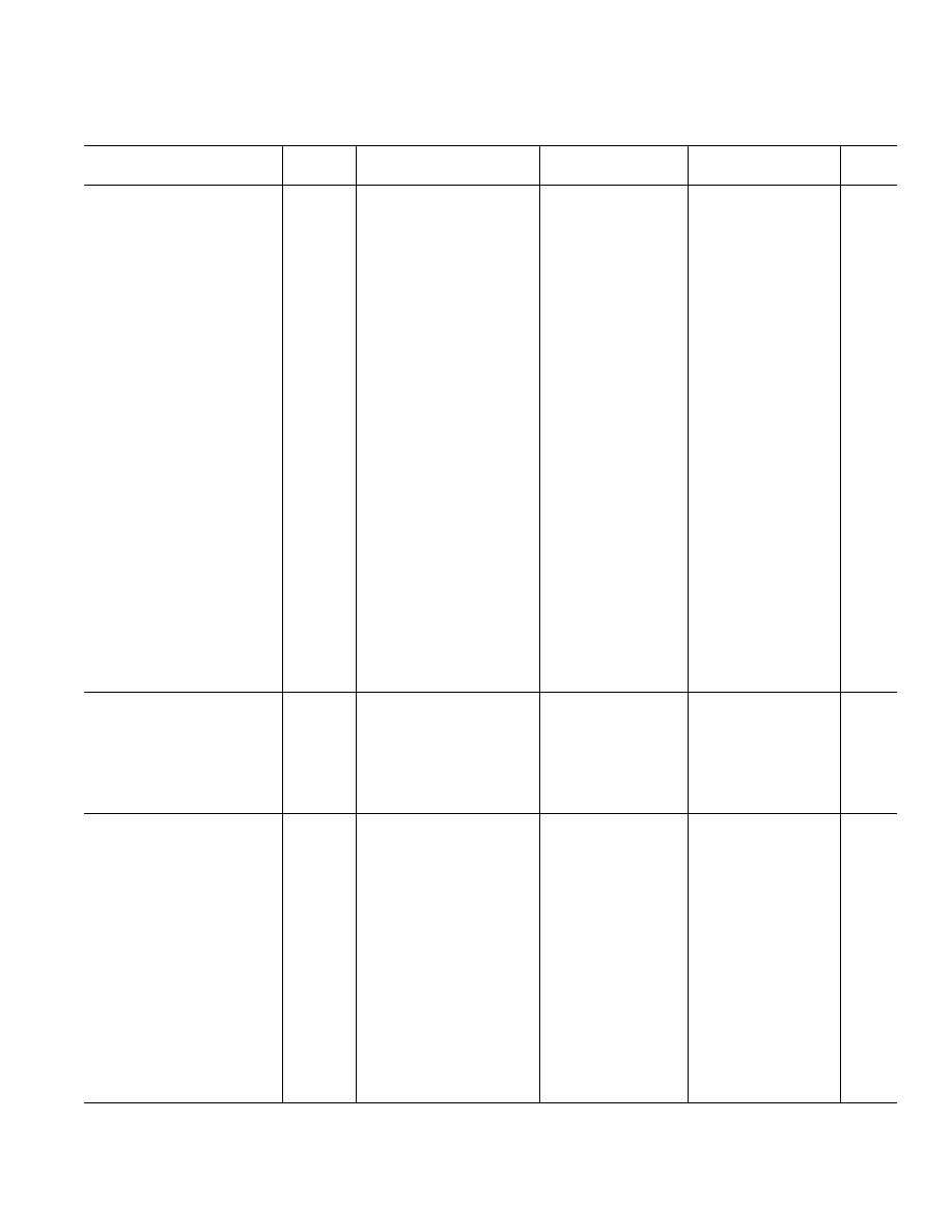
20-Lead SOIC
TOP VIEW
(Not to Scale)
20
19
18
17
16
15
14
13
12
11
1
2
3
4
5
6
7
8
9
10
AMP01
≠V
OP
OUTPUT
REFERENCE
TEST PIN*
≠IN
V
OOS
NULL
SENSE
TEST PIN*
V
OOS
NULL
V≠
V+
+V
OP
TEST PIN*
+IN
V
IOS
NULL
R
S
R
S
R
G
R
G
V
IOS
NULL
*MAKE NO ELECTRICAL CONNECTION
FEATURES
Low Offset Voltage: 50 V Max
Very Low Offset Voltage Drift: 0.3 V/ C Max
Low Noise: 0.12 V p-p (0.1 Hz to 10 Hz)
Excellent Output Drive: 10 V at 50 mA
Capacitive Load Stability: to 1 F
Gain Range: 0.1 to 10,000
Excellent Linearity: 16-Bit at G = 1000
High CMR: 125 dB min (G = 1000)
Low Bias Current: 4 nA Max
May Be Configured as a Precision Op Amp
Output-Stage Thermal Shutdown
Available in Die Form
*Protected under U.S. Patent Numbers 4,471,321 and 4,503,381.
One Technology Way, P.O. Box 9106, Norwood, MA 02062-9106, U.S.A.
Tel: 781/329-4700
World Wide Web Site: http://www.analog.com
Fax: 781/326-8703
© Analog Devices, Inc., 1999
REV. D
≠2≠
AMP01≠SPECIFICATIONS
ELECTRICAL CHARACTERISTICS
(@ V
S
= 15 V, R
S
= 10 k , R
L
= 2 k , T
A
= +25 C, unless otherwise noted)
AMP01A
AMP01B
Parameter
Symbol
Conditions
Min
Typ
Max
Min
Typ
Max
Units
OFFSET VOLTAGE
Input Offset Voltage
V
IOS
T
A
= +25
∞
C
20
50
40
100
µ
V
≠55
∞
C
T
A
+125
∞
C
40
80
60
150
µ
V
Input Offset Voltage Drift
TCV
IOS
≠55
∞
C
T
A
+125
∞
C
0.15
0.3
0.3
1.0
µ
V/
∞
C
Output Offset Voltage
V
OOS
T
A
= +25
∞
C
1
3
2
6
mV
≠55
∞
C
T
A
+125
∞
C
3
6
6
10
mV
Output Offset Voltage Drift
TCV
OOS
R
G
=
≠55
∞
C
T
A
+125
∞
C
20
50
50
120
µ
V/
∞
C
Offset Referred to Input
PSR
G = 1000
120
130
110
120
dB
vs. Positive Supply
G = 100
110
130
100
120
dB
V+ = +5 V to +15 V
G = 10
95
110
90
100
dB
G = 1
75
90
70
80
dB
≠55
∞
C
T
A
+125
∞
C
G = 1000
120
130
110
120
dB
G = 100
110
130
100
120
dB
G = 10
95
110
90
100
dB
G = 1
75
90
70
80
dB
Offset Referred to Input
PSR
G = 1000
105
125
105
115
dB
vs. Negative Supply
G = 100
90
105
90
95
dB
V≠ = ≠5 V to ≠15 V
G = 10
70
85
70
75
dB
G = 1
50
65
50
60
dB
≠55
∞
C
T
A
+125
∞
C
G = 1000
105
125
105
115
dB
G = 100
90
105
90
95
dB
G = 10
70
85
70
75
dB
G = 1
50
85
50
60
dB
Input Offset Voltage Trim
Range
V
S
=
±
4.5 V to
±
18 V
1
±
6
±
6
mV
Output Offset Voltage Trim
Range
V
S
=
±
4.5 V to
±
18 V
1
±
100
±
100
mV
INPUT CURRENT
Input Bias Current
I
B
T
A
= +25
∞
C
1
4
2
6
nA
≠55
∞
C
T
A
+125
∞
C
4
10
6
15
nA
Input Bias Current Drift
TCI
B
≠55
∞
C
T
A
+125
∞
C
40
50
pA/
∞
C
Input Offset Current
I
OS
T
A
= +25
∞
C
0.2
1.0
0.5
2.0
nA
≠55
∞
C
T
A
+125
∞
C
0.5
3.0
1.0
6.0
nA
Input Offset Current Drift
TCI
OS
≠55
∞
C
T
A
+125
∞
C
3
5
pA/
∞
C
INPUT
Input Resistance
R
IN
Differential, G = 1000
1
1
G
Differential, G
100
10
10
G
Common Mode, G = 1000
20
20
G
Input Voltage Range
IVR
T
A
= +25
∞
C
2
±
10.5
±
10.5
V
≠55
∞
C
T
A
+125
∞
C
±
10.0
±
10.0
V
Common-Mode Rejection
CMR
V
CM
=
±
10 V, 1 k
Source Imbalance
G = 1000
125
130
115
125
dB
G = 100
120
130
110
125
dB
G = 10
100
120
95
110
dB
G = 1
85
100
75
90
dB
≠55
∞
C
T
A
+125
∞
C
G = 1000
120
125
110
120
dB
G = 100
115
125
105
120
dB
G = 10
95
115
90
105
dB
G = 1
80
95
75
90
dB
NOTES
1
V
IOS
and V
OOS
nulling has minimal affect on TCV
IOS
and TCV
OOS
respectively.
2
Refer to section on common-mode rejection.
Specifications subject to change without notice.
ELECTRICAL CHARACTERISTICS
AMP01E
AMP01F/G
Parameter
Symbol
Conditions
Min
Typ
Max
Min
Typ
Max
Units
OFFSET VOLTAGE
Input Offset Voltage
V
IOS
T
A
= +25
∞
C
20
50
40
100
µ
V
T
MIN
T
A
T
MAX
40
80
60
150
µ
V
Input Offset Voltage Drift
TCV
IOS
T
MIN
T
A
T
MAX
1
0.15
0.3
0.3
1.0
µ
V/
∞
C
Output Offset Voltage
V
OOS
T
A
= +25
∞
C
1
3
2
6
mV
T
MIN
T
A
T
MAX
3
6
6
10
mV
Output Offset Voltage Drift
TCV
OOS
R
G
=
1
T
MIN
T
A
T
MAX
20
100
50
120
µ
V/
∞
C
Offset Referred to Input
PSR
G = 1000
120
130
110
120
dB
vs. Positive Supply
G = 100
110
130
100
120
dB
V+ = +5 V to +15 V
G = 10
95
110
90
100
dB
G = 1
75
90
70
80
dB
T
MIN
T
A
T
MAX
G = 1000
120
130
110
120
dB
G = 100
110
130
100
120
dB
G = 10
95
110
90
100
dB
G = 1
75
90
70
80
dB
Offset Referred to Input
PSR
G = 1000
110
125
105
115
dB
vs. Negative Supply
G = 100
95
105
90
95
dB
V≠ = ≠5 V to ≠15 V
G = 10
75
85
70
75
dB
G = 1
55
65
50
60
dB
T
MIN
T
A
T
MAX
G = 1000
110
125
105
115
dB
G = 100
95
105
90
95
dB
G = 10
75
85
70
75
dB
G = 1
55
85
50
60
dB
Input Offset Voltage Trim
Range
V
S
=
±
4.5 V to
±
18 V
2
±
6
±
6
mV
Output Offset Voltage Trim
Range
V
S
=
±
4.5 V to
±
18 V
2
±
100
±
100
mV
INPUT CURRENT
Input Bias Current
I
B
T
A
= +25
∞
C
1
4
2
6
mV
T
MIN
T
A
T
MAX
4
10
6
15
mV
Input Bias Current Drift
TCI
B
T
MIN
T
A
T
MAX
40
50
pA/
∞
C
Input Offset Current
I
OS
T
A
= +25
∞
C
0.2
1.0
0.5
2.0
mV
T
MIN
T
A
T
MAX
0.5
3.0
1.0
6.0
mV
Input Offset Current Drift
TCI
OS
T
MIN
T
A
T
MAX
3
5
pA/
∞
C
INPUT
Input Resistance
R
IN
Differential, G = 1000
1
1
G
Differential, G
100
10
10
G
Common Mode, G = 1000
20
20
G
Input Voltage Range
IVR
T
A
= +25
∞
C
3
±
10.5
±
10.5
V
T
MIN
T
A
T
MAX
±
10.0
±
10.0
V
Common-Mode Rejection
CMR
V
CM
=
±
10 V, 1 k
Source Imbalance
G = 1000
125
130
115
125
dB
G = 100
120
130
110
125
dB
G = 10
100
120
95
110
dB
G = 1
85
100
75
90
dB
T
MIN
T
A
T
MAX
G = 1000
120
125
110
120
dB
G = 100
115
125
105
120
dB
G = 10
95
115
90
105
dB
G = 1
80
95
75
90
dB
NOTES
1
Sample tested.
2
V
IOS
and V
OOS
nulling has minimal affect on TCV
IOS
and TCV
OOS
, respectively.
3
Refer to section on common-mode rejection.
Specifications subject to change without notice.
(@ V
S
= 15 V, R
S
= 10 k , R
L
= 2 k
, T
A
= +25 C, ≠25 C
T
A
+85 C for E, F
grades, 0 C
T
A
+70 C for G grade, unless otherwise noted)
AMP01
≠3≠
REV. D

AMP01
≠4≠
REV. D
ELECTRICAL CHARACTERISTICS
(@ V
S
= 15 V, R
S
= 10 k , R
L
= 2 k , T
A
= +25 C, unless otherwise noted)
AMP01A/E
AMP01B/F/G
Parameter
Symbol Conditions
Min
Typ
Max
Min
Typ
Max
Units
GAIN
Gain Equation Accuracy
G =
20
◊
R
S
R
G
0.3
0.6
0.5
0.8
%
Accuracy Measured
from G = 1 to 1000
Gain Range
G
0.1
10k
0.1
10k
V/V
Nonlinearity
G = 1000
1
0.0007 0.005
0.0007 0.005
%
G = 100
1
0.005
0.005
%
G = 10
1
0.005
0.007
%
G = 1
1
0.010
0.015
%
Temperature Coefficient
G
TC
1
G
1000
1, 2
5
10
5
15
ppm
∞
C
OUTPUT RATING
Output Voltage Swing
V
OUT
R
L
= 2 k
±
13.0
±
13.8
±
13.0
±
13.8
V
R
L
= 500
±
13.0
±
13.5
±
13.0
±
13.5
V
R
L
= 50
±
2.5
±
4.0
±
2.5
±
4.0
V
R
L
= 2 k
Over Temp.
±
12.0
±
13.8
±
12.0
±
13.8
V
R
L
= 500
3
±
12.0
±
13.5
±
12.0
±
13.5
V
Positive Current Limit
Output-to-Ground Short
60
100
120
60
100
120
mA
Negative Current Limit
Output-to-Ground Short
60
90
120
60
90
120
mA
Capacitive Load Stability
1
G
1000
No Oscillations
1
0.1
1
0.1
1
µ
F
Thermal Shutdown
Temperature
Junction Temperature
165
165
∞
C
NOISE
Voltage Density, RTI
e
n
f
O
= 1 kHz
e
n
G = 1000
5
5
nV/
Hz
e
n
G = 100
10
10
nV/
Hz
e
n
G = 10
59
59
nV/
Hz
e
n
G = 1
540
540
nV/
Hz
Noise Current Density, RTI
i
n
f
O
= 1 kHz, G = 1000
0.15
0.15
pA/
Hz
Input Noise Voltage
e
n
p-p
0.1 Hz to 10 Hz
e
n
p-p
G = 1000
0.12
0.12
µ
V p-p
e
n
p-p
G = 100
0.16
0.16
µ
V
p-p
e
n
p-p
G = 10
1.4
1.4
µ
V p-p
e
n
p-p
G = 1
13
13
µ
V p-p
Input Noise Current
i
n
p-p
0.1 Hz to 10 Hz, G = 1000
2
2
pA p-p
DYNAMIC RESPONSE
Small-Signal
G = 1
570
570
kHz
Bandwidth (≠3 dB)
BW
G = 10
100
100
kHz
G = 100
82
82
kHz
G = 1000
26
26
kHz
Slew Rate
SR
G = 10
3.5
4.5
3.0
4.5
V/
µ
s
Settling Time
t
S
To 0.01%, 20 V step
G = 1
12
12
µ
s
G = 10
13
13
µ
s
G = 100
15
15
µ
s
G = 1000
50
50
µ
s
NOTES
1
Guaranteed by design.
2
Gain tempco does not include the effects of gain and scale resistor tempco match.
3
≠55
∞
C
T
A
+125
∞
C for A/B grades, ≠25
∞
C
T
A
+85
∞
C for E/F grades, 0
∞
C
T
A
70
∞
C for G grades.
Specifications subject to change without notice.

ORDERING GUIDE
Model
Temperature Range
Package Description Package Option
AMP01AX
≠55
∞
C to +125
∞
C
18-Lead Cerdip
Q-18
AMP01AX/883C
≠55
∞
C to +125
∞
C
18-Lead Cerdip
Q-18
AMP01BTC/883C
≠55
∞
C to +125
∞
C
28-Terminal LCC
E-28A
AMP01BX
≠55
∞
C to +125
∞
C
18-Lead Cerdip
Q-18
AMP01BX/883C
≠55
∞
C to +125
∞
C
18-Lead Cerdip
Q-18
AMP01EX
≠25
∞
C to +85
∞
C
18-Lead Cerdip
Q-18
AMP01FX
≠25
∞
C to +85
∞
C
18-Lead Cerdip
Q-18
AMP01GBC
Die
AMP01GS
0
∞
C to +70
∞
C
20-Lead SOIC
R-20
AMP01GS-REEL
0
∞
C to +70
∞
C
13
" Tape and Reel
R-20
AMP01NBC
Die
5962-8863001VA* ≠55
∞
C to +125
∞
C
18-Lead Cerdip
Q-18
5962-88630023A* ≠55
∞
C to +125
∞
C
28-Terminal LCC
E-28A
5962-8863002VA* ≠55
∞
C to +125
∞
C
18-Lead Cerdip
Q-18
*Standard military drawing available.
ELECTRICAL CHARACTERISTICS
(@ V
S
= 15 V, R
S
= 10 k , R
L
= 2 k , T
A
= +25 C, unless otherwise noted)
AMP01A/E
AMP01B/F/G
Parameter
Symbol Conditions
Min
Typ
Max
Min
Typ
Max
Units
SENSE INPUT
Input Resistance
R
IN
35
50
65
35
50
65
k
Input Current
I
IN
Referenced to V≠
280
280
µ
A
Voltage Range
(Note 1)
≠10.5
+15
≠10.5
+15
V
REFERENCE INPUT
Input Resistance
R
IN
35
50
65
35
50
65
k
Input Current
I
IN
Referenced to V≠
280
280
µ
A
Voltage Range
(Note 1)
≠10.5
+15
≠10.5
+15
V
Gain to Output
1
1
V/V
POWER SUPPLY ≠25
∞
C
T
A
+85
∞
C for E/F Grades, ≠55
∞
C
T
A
+125
∞
C for A/B Grades
Supply Voltage Range
V
S
+V linked to +V
OP
±
4.5
±
18
±
4.5
±
18
V
V
S
≠V linked to ≠V
OP
±
4.5
±
18
±
4.5
±
18
V
Quiescent Current
I
Q
+V linked to +V
OP
3.0
4.8
3.0
4.8
mA
I
Q
≠V linked to ≠V
OP
3.4
4.8
3.4
4.8
mA
NOTE
1
Guaranteed by design.
Specifications subject to change without notice.
AMP01
≠5≠
REV. D
1. R
G
2. R
G
3. ≠INPUT
4. V
OOS
NULL
5. V
OOS
NULL
6. TEST PIN*
7. SENSE
8. REFERENCE
9. OUTPUT
10. V≠ (OUTPUT)
11. V≠
12. V+
13. V+ (OUTPUT)
14. R
S
15. R
S
16. V
IOS
NULL
17. V
IOS
NULL
18. +INPUT
* MAKE NO ELECTRICAL CONNECTION
DICE CHARACTERISTICS
Die Size 0.111
◊
0.149 inch, 16,539 sq. mils
(2.82
◊
3.78 mm, 10.67 sq. mm)