
REV. C
Information furnished by Analog Devices is believed to be accurate and
reliable. However, no responsibility is assumed by Analog Devices for its
use, nor for any infringements of patents or other rights of third parties
which may result from its use. No license is granted by implication or
otherwise under any patent or patent rights of Analog Devices.
a
AD846
One Technology Way, P.O. Box 9106, Norwood, MA 02062-9106, U.S.A.
Tel: 781/329-4700
World Wide Web Site: http://www.analog.com
Fax: 781/326-8703
© Analog Devices, Inc., 2000
450 V/ s, Precision,
Current-Feedback Op Amp
CONNECTION DIAGRAMS
FEATURES
AC PERFORMANCE
Small Signal Bandwidth: 80 MHz (A
V
= ≠1)
Slew Rate: 450 V/ s
Full Power Bandwidth: 6.8 MHz at 20 V p-p,
R
L
= 500
Fast Settling: for 10 V Step: 110 ns to 0.01%,
80 ns to 0.1%
Differential Gain: <0.01% @ 4.4 MHz
Differential Phase: <0.028 @ 4.4 MHz
Total Harmonic Distortion (THD): 0.0005% @ 100 kHz
Open-Loop Transimpedance: 200 M
Input Voltage Noise: 2 nV/
Hz
DC PERFORMANCE
Input Offset Voltage: 75 V max (B Grade)
Input Offset Drift: 3.5 V/ C max (B Grade)
Quiescent Supply Current: 6.5 mA max
APPLICATIONS
High Speed DAC Buffers
Multiflash ADC Error Amplifiers
Flash ADC Buffers
Coaxial Cable Drivers
High Performance Audio Circuitry
Available in Plastic Mini-DIP, Hermetic Cerdip, and
Plastic SOIC (A) Package
MIL-STD-883B Part Available
PRODUCT DESCRIPTION
The AD846 is a monolithic, very high speed operational ampli-
fier offering high performance. Although technically classed as a
current-feedback or transimpedance amplifier, it may be used
in much the same way as traditional op amps while providing
significant performance benefits. Employing Analog Devices'
junction isolated complementary bipolar (CB) process, the AD846
achieves true "12-bit" (0.01%) precision on critical ac and dc
parameters, a level of performance unmatched by amplifiers
fabricated using either the dielectrically isolated (DI) or other
bipolar processes.
The AD846 offers significant advantages over conventional
high speed operational amplifiers. It maintains a nearly con-
stant bandwidth and settling time to 0.01% over a wide range
of closed-loop gains. This makes the AD846 ideal for amplifying
the residue in multiple-pass analog-to-digital converters.
Other advantages include: low input errors and high open-loop
transresistance (200 M
) into a 500 load, ensuring true
12-bit dc accuracy for closed-loop gains from ≠1 to gains
greater than ≠100. This combination of ac and dc perfor-
mance makes the AD846 an excellent choice for buffering
precision high speed DACs and flash ADCs.
Plastic Mini-DIP (N) Package
and
Cerdip (Q) Package
The AD846 is available in three performance grades. The AD846A
and AD846B are rated over the industrial temperature range
of ≠40
∞C to +85∞C. The AD846S is rated over the full mili-
tary temperature range of ≠55
∞C to +125∞C and is available
processed to MIL-STD-883B, Rev C.
The AD846 is available in two types of 8-lead packages: plastic
mini-DIP and hermetic cerdip. The AD846AR-16 is available in
the 16-lead SOIC package. "A" and "S" grade chips are also
available.
PRODUCT HIGHLIGHTS
1. The AD846 achieves settling times of 110 ns to 0.01%
for gains of ≠1 to ≠10, with a 450 V/
µs slew rate, while
consuming only 5 mA of supply current.
2. For closed-loop gains of ≠1 to ≠100, the high speed perfor-
mance of the AD846 is achieved without sacrificing full 12-bit
dc precision.
3. The AD846 is well suited to line driver and video buffer
applications where the properties of low distortion and high
slew rate are required.
SOIC (R) Package
16
15
14
13
12
11
10
9
1
2
3
4
5
6
7
8
NC = NO CONNECT
NC
NC
≠INPUT
NC
+INPUT
NC
≠V
S
NC
NC
NC
+V
S
NC
OUTPUT
COMPENSATION
NC
NC
TOP VIEW
(Not to Scale)
AD846
≠
+

REV. C
≠2≠
AD846≠SPECIFICATIONS
(@ +25 C and 15 V dc, unless otherwise noted)
AD846A
AD846B
AD846S
Model
Conditions
Min
Typ
Max
Min
Typ
Max
Min
Typ
Max
Units
INPUT OFFSET VOLTAGE
1
Initial
25
200
25
75
25
200
µV
T
MIN
≠T
MAX
50
350
50
125
100
350
µV
vs. Temperature
0.8
5
0.8
3.5
1
5.5
µV/∞C
vs. Supply (PSRR)
5 V≠18 V
2
Initial
110
125
120
125
110
125
dB
T
MIN
≠T
MAX
110
120
116
120
94
116
dB
vs. Common Mode (CMRR)
V
CM
=
± 10 V
Initial
110
125
120
125
110
125
dB
T
MIN
≠T
MAX
110
120
116
120
94
116
dB
INPUT BIAS CURRENT
3
≠Input Bias Current
Initial
150
450
100
250
150
450
nA
T
MIN
≠T
MAX
450
1200
400
750
1000
1500
nA
vs. Temperature
6
20
6
17
9
20
nA/
∞C
vs. Supply
5 V≠18 V
2
Initial
9
15
9
10
9
15
nA/V
T
MIN
≠T
MAX
11
20
11
15
11
25
nA/V
vs. Common Mode
V
CM
=
± 10 V
Initial
5
10
3
5
5
10
nA/V
T
MIN
≠T
MAX
5
15
3
7
5
20
nA/V
+Input Bias Current
Initial
3
15
3
5
3
15
µA
T
MIN
≠T
MAX
4
20
4
7
5
20
µA
vs. Temperature
15
80
15
45
15
80
nA/
∞C
vs. Supply
5 V≠18 V
2
Initial
5
15
5
10
5
15
nA/V
T
MIN
≠T
MAX
5
20
5
15
5
20
nA/V
vs. Common Mode
V
CM
=
± 10 V
Initial
5
15
3
10
5
15
nA/V
T
MIN
≠T
MAX
5
15
3
10
5
20
nA/V
INPUT CHARACTERISTICS
Input Resistance
≠Input
50
50
50
+Input
10
10
10
k
Input Capacitance
≠Input
2
2
2
pF
+Input
2
2
2
pF
INPUT VOLTAGE RANGE
Common Mode
±10
±10
±10
V
INPUT VOLTAGE NOISE
F = 1 kHz
2
2
2
nV/
Hz
Input Current Noise
≠Input
1 kHz
20
20
20
pA/
Hz
+Input
1 kHz
6
6
6
pA/
Hz
OPEN LOOP
TRANSRESISTANCE
V
OUT
=
±10 V
R
LOAD
= 500
100
200
150
200
100
200
M
T
MIN
≠T
MAX
50
75
50
M
OUTPUT CHARACTERISTICS
Voltage
R
LOAD
= 500
10
10
10
V
Current
Short Circuit
65
65
65
mA
Output Resistance
Open Loop
16
16
16
FREQUENCY RESPONSE
Small Signal Bandwidth
A
V
= ≠1 R
F
= 1k
80
80
80
MHz
(≠3 dB)
A
V
= ≠10 R
F
= 875
31
31
31
MHz
A
V
= ≠30 R
F
= 875
15
15
15
MHz
Full Power Bandwidth
4
V
OUT
= 20 V p-p
R
I
= 500
6.8
6.8
6.8
MHz
Rise Time
A
V
= ≠1
110
10
10
ns
Overshoot
A
V
= ≠1
20
20
20
%
Slew Rate
A
V
= ≠1
450
450
450
V/
µs
Settling Time
10 V Step, A
V
= ≠1
to 0.1%
80
80
80
ns
to 0.01%
110
110
110
ns
TOTAL HARMONIC
DISTORTION
5
F = 100 kHz
0.0005
0.0005
0.0005
%

REV. C
≠3≠
AD846
ORDERING GUIDE
Package
Model
1
Temperature Range
Option
2
AD846AN
≠40
∞C to +85∞C
N-8
AD846BN
≠40
∞C to +85∞C
N-8
AD846AQ
≠40
∞C to +85∞C
Q-8
AD846BQ
≠40
∞C to +85∞C
Q-8
AD846SQ
≠55
∞C to +125∞C
Q-8
AD846SQ/883B
≠55
∞C to +125∞C
Q-8
5962-8964601PA
≠55
∞C to +125∞C
Q-8
AD846AR-16
≠40
∞C to +85∞C
R-16
AD846AR-16-REEL
≠40
∞C to +85∞C
R-16
NOTES
1
"A" and "S" grade chips are also available.
2
N = Plastic DIP Package; Q = Cerdip Package, R = SOIC Package
METALIZATION PHOTOGRAPH
Dimensions shown in inches and (mm).
Consult factory for latest dimensions.
AD846A
AD846B
AD846S
Model
Conditions
Min
Typ
Max
Min
Typ
Max
Min
Typ
Max
Units
DIFFERENTIAL GAIN
F = 4.4 MHz, R
L
= 100
0.01
0.01
0.01
%
DIFFERENTIAL PHASE
F = 4.4 MHz, R
L
= 100
0.028
0.028
0.028
Degrees
POWER SUPPLY
Rated Performance
±15
±15
±15
V
Operating Range
±5
18
±5
18
5
18
V
Quiescent Current
T
MIN
≠T
MAX
5
6.5
5
6.5
5
7
mA
TRANSISTOR COUNT
72
72
72
NOTES
1
Input Offset Voltage Specifications are guaranteed after 5 minutes at T
A
= +25
∞C.
2
Test Conditions: +V
S
= 15 V, ≠V
S
= 5 V to 18 V and +V
S
= 5 V to 18 V, ≠V
S
= 15 V.
3
Bias Current Specifications are guaranteed maximum after 5 minutes at T
A
= +25
∞C.
4
FPBW = Slew Rate/2
V
PEAK
.
5
Total Harmonic Distortion.
All min and max specifications are guaranteed. Specifications shown in boldface are tested on all production units at final electrical test. Results from those tests are
used to calculate outgoing quality levels.
Specifications subject to change without notice.
ABSOLUTE MAXIMUM RATINGS
1
Supply Voltage . . . . . . . . . . . . . . . . . . . . . . . . . . . . . . .
±18 V
Internal Power Dissipation
2
Plastic Package . . . . . . . . . . . . . . . . . . . . . . . . . . . . . . 1.5 W
Cerdip Package . . . . . . . . . . . . . . . . . . . . . . . . . . . . . 1.3 W
Common-Mode Input Voltage, Max Safe . . . . . . . |V
S
| ≠ 3 V
Output Short Circuit Duration . . . . . . . . . . . . . . . . Indefinite
Differential Input Voltage . . . . . . . . . . . . . . . . . . . . . . .
±1 V
Continuous Input Current
Inverting or Noninverting . . . . . . . . . . . . . . . . . . . . 2.0 mA
Storage Temperature Range (Q) . . . . . . . . . ≠65
∞C to +150∞C
Storage Temperature Range (N) . . . . . . . . . ≠65
∞C to +125∞C
Storage Temperature Range (R) . . . . . . . . . ≠65
∞C to +125∞C
Operating Temperature Range
AD846A/B . . . . . . . . . . . . . . . . . . . . . . . . ≠40
∞C to +85∞C
AD846S . . . . . . . . . . . . . . . . . . . . . . . . . . ≠55
∞C to +125∞C
Lead Temperature Range (Soldering 60 sec) . . . . . . . +300
∞C
ESD Rating . . . . . . . . . . . . . . . . . . . . . . . . . . . . . . . . . 3500 V
NOTES
1
Stresses above those listed under Absolute Maximum Ratings may cause perma-
nent damage to the device. This is a stress rating only; the functional operation of
the device at these or any other conditions above those indicated in the operational
sections of this specification is not implied. Exposure to absolute maximum rating
conditions for extended periods may affect device reliability.
2
Maximum internal power dissipation is specified so that T
J
does not exceed
+175
∞C at an ambient temperature of +25∞C, derate cerdip (Q) package at
8.7 mW/
∞C and plastic (N) package at 10 mW/∞C.
Plastic Package:
JA
= 100
∞C/Watt,
JC
= 33
∞C/W.
Cerdip Package:
JA
= 110
∞C/Watt,
JC
= 30
∞C/W.
SOIC Package:
JA
= 100
∞C/Watt,
JC
= 33
∞C/W.

REV. C
AD846 ≠ Typical Characteristics
≠4≠
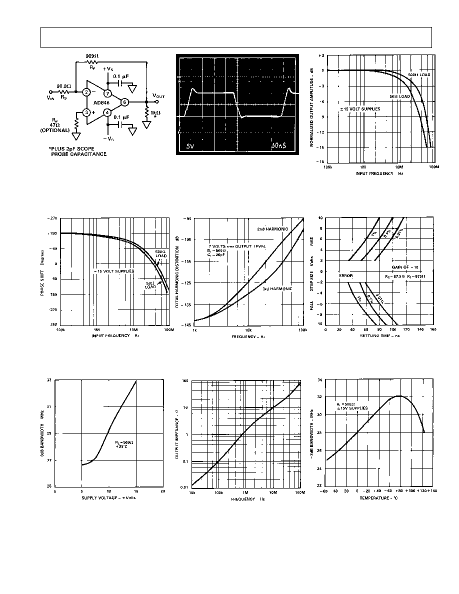
Figure 1. Input Voltage Swing
vs. Supply
Figure 4. Quiescent Supply Current
vs. Temperature
Figure 7. Open-Loop Transimpedance
vs. Supply
Figure 2. Output Voltage Swing
vs. Supply
Figure 5. Output Voltage Swing vs.
Resistive Load
Figure 8. Positive Input Bias Current
vs. Common-Mode Voltage
Figure 3. Quiescent Current vs.
Supply Voltage
Figure 6. Large Signal Frequency
Response
Figure 9. Negative Input Bias
Current vs. Common-Mode Voltage

REV. C
AD846
≠5≠
Figure 10. Positive Input Bias Current
vs. Temperature
Figure 13. Common-Mode Rejection
vs. Frequency
Figure 16. Short Circuit Current Limit
vs. Temperature
Figure 11. Negative Input Bias
Current vs. Temperature
Figure 14. Input Noise Voltage
Spectral Density
Figure 17. Slew Rate vs.
Temperature
Figure 12. Power Supply Rejection
vs. Frequency
Figure 15. Inverting Input Noise
Current Spectral Density
Figure 18. Slew Rate vs. Input
Error Signal

REV. C
AD846 ≠ Typical Characteristics
≠6≠
Figure 19a. Inverting Amplifier,
Gain of 1
Figure 21. Phase Shift vs. Frequency
Figure 24. 3 dB Bandwidth vs.
Supply Voltage
Figure 19b. Large Signal Pulse
Response, Gain of ≠1
Figure 22. Total Harmonic Distortion
vs. Frequency
Figure 25. Output Impedance
vs. Frequency
Figure 20. Normalized Output
Amplitude vs. Frequency vs. Load
Figure 23. Settling Time
vs. Step Size
Figure 26. ≠3 dB Bandwidth
vs. Temperature
, Inverting Gain of 1
REV. C
AD846
≠7≠
Typical Characteristics, Inverting Gain of 10 ≠
Figure 27a. Inverting Amplifier,
Gain of 10
Figure 29. Phase vs. Frequency
vs. Load
Figure 32. 3 dB Bandwidth vs.
Supply Voltage
Figure 27b. Large Signal Pulse
Response, Gain of 10
Figure 30. Harmonic Distortion
vs. Frequency
Figure 33. Output Impedance
vs. Frequency
Figure 28. Normalized Output
Amplitude vs. Frequency vs. Load
Figure 31. Settling Time vs.
Step Size
Figure 34. ≠3 dB Bandwidth
vs. Temperature

REV. C
AD846
≠8≠
POWER SUPPLY CONSIDERATIONS
The power supply connections to the AD846 must maintain a
low impedance to ground over a bandwidth of 40 MHz or more.
This is especially important when driving a significant resistive
or capacitive load, since all current delivered to the load comes
from the power supplies. Multiple high quality bypass capacitors
are recommended for each power supply line in any critical
application. A 0.1
µF ceramic and a 2.2 µF electrolytic capacitor
as shown in Figure 35 placed as close as possible to the am-
plifier (with short lead lengths to power supply common) will
assure adequate high frequency bypassing, in most applications.
A minimum bypass capacitance of 0.1
µF should be used for any
application.
Figure 35. Recommended Power Supply Bypassing
THEORY OF OPERATION
The AD846 differs from conventional operational amplifiers
in that it is a transimpedance device rather than a conventional
voltage amplifier. Figure 36 is a simplified schematic of the
AD846. The input stage consists of a pair of transistors, Q1 and
Q2, which are biased by two diode-connected transistors, Q3
and Q4. Transistors Q1 and Q2 have their emitters connected
together, and this common point functions as the inverting in-
put of the amplifier. Correspondingly, the common connection
of the two biasing diodes acts as the noninverting input.
Figure 36. AD846 Simplified Schematic
When operated as a closed-loop amplifier, feedback error cur-
rent, I
IN
: flows into the inverting input terminal and is conveyed
via current mirrors (transistors Q5, Q6, Q7, and Q8) to the
compensation capacitor, C
COMP
. The voltage developed across
C
COMP
is buffered by the output stage, consisting of transistors
Q9≠Q12.
Figure 37. Overload Recovery Test Circuit
Figure 38. Overload Recovery Time Photo
Because the input error signal developed is in the form of a
current, not a voltage, the AD846 differs from conventional
operational amplifiers. This also means that, unlike most opera-
tional amplifiers which rely on negative feedback to produce a
"virtual ground" at the inverting input terminal, this terminal
explicitly has a low impedance.
A unique circuit approach allows the AD846 to realize an open-
loop transimpedance of close to 200 M
. This is nearly three
orders of magnitude greater than that of any other operational
transimpedance amplifier and results in extremely high levels of
dc precision.
As an example, the output voltage gain error is approximately
equal to the value of the feedback resistor divided by the value
of the open-loop transimpedance of the amplifier. That is, when
using a 1 k
feedback resistor, this error is one part in 200,000.
For a transimpedance amplifier with 1 M
transimpedance, this
error is only one part in 1000; such an amplifier would barely be
able to achieve 10-bit precision.
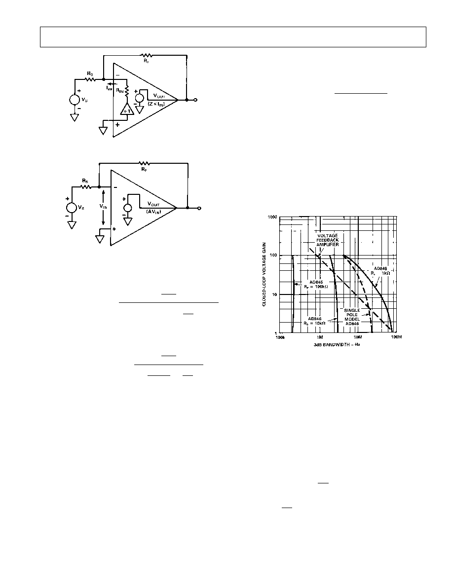
Figure 39 is a simplified three-terminal model for the AD846.
Figure 40 is a simplified three-terminal model for a conventional
voltage op amp. The action of current feedback serves to modify
the behavior of the amplifier under closed-loop conditions. The
feedback resistor, R
F
, is somewhat analogous to the input stage
transconductance of a conventional voltage amplifier; and
therefore, if the value of R
F
is held constant, the closed-loop
bandwidth also remains virtually constant, independent of
closed-loop voltage gain.
REV. C
AD846
≠9≠
Figure 39. AD846 Three-Terminal Model
Figure 40. Op Amp Three-Terminal Model
A more detailed examination of the closed-loop transfer func-
tion of the AD846 results in the following equation:
Closed-Loop Gain G(s) =
-R
F
R
S
1
+ C
COMP
R
F
+ 1+
R
F
R
S
R
IN
s
Compare this to the equation for a conventional op amp:
Closed-Loop Gain G(s) =
-R
F
R
S
1
+
C
COMP
g
M
1
+
R
F
R
S
s
where: C
COMP
is the internal compensation capacitor of the am-
plifier; g
M
is the input stage transconductance of the amplifier.
In the case of the voltage amplifier, the closed-loop bandwidth
decreases directly with increasing values of (1 + R
F
/R
S
), the
closed-loop gain. However, for the transimpedance amplifier,
the situation is different. At low gains, where (1 + R
F
/R
S
) R
IN
is
small compared to R
F
, the closed-loop bandwidth is controlled
by the internal compensation capacitance of 7 pF and the value
of R
F
, and not by the closed-loop gain. At higher gains, where (1
+ R
F
/R
S
) R
IN
is much larger than R
F
, the behavior is that of a con-
ventional operational amplifier in which the input stage transcon-
ductance is equal to the inverting terminal input impedance of
the transimpedance amplifier (R
IN
= 50
).
A simple equation can, therefore, be used to determine the band-
width of an amplifier employing the AD846 in the inverting
configuration.
3 dB Bandwidth
=
23
R
F
+ 0.05 1+ G
(
)
where: The 3 dB bandwidth is in MHz
G is the closed-loop inverting gain of the AD846
R
F
is the feedback resistance in k
.
NOTE: This equation applies only for values of R
F
between
10 k
and 100 k, and for R
LOAD
greater than 500
. For R
F
=
1 k
the bandwidth should be estimated from Figure 41.
Figure 41 illustrates the closed-loop voltage gain vs. frequency
of the AD846 for various values of feedback resistor. For com-
parison purposes, the characteristic of a conventional amplifier
having an 80 MHz unity gain bandwidth is also shown.
Figure 41. Closed-Loop Voltage Gain vs. Bandwidth for
Various Values of R
F
For the case where R
F
= 1 k
and R
S
= 100
(closed-loop gain
of ≠10), the closed-loop bandwidth is approximately 28 MHz. It
should also be noted that the use of a capacitor to shunt R
F
, a
normal practice for stabilizing conventional op amps, will cause
this amplifier to become unstable because the closed-loop band-
width will increase beyond the stable operating frequency.
A similar approach can be taken to calculate the noise perfor-
mance of the amplifier. A simplified noise model is shown in
Figure 42.
The equivalent mean-square output noise voltage spectral den-
sity will equal:
V
ON
2
= R
F
I
NN
(
)
2
+ 1+
R
F
R
S
2
[V
N
2
+ R
P
I
NP
(
)
2
+ 4 kT R
P
]
+ 4 kT R
F
R
F
R
S
+1

REV. C
AD846
≠10≠
Where:
R
P
is the external resistance placed in series with the non-
inverting input
R
F
is the feedback resistor
R
S
is the source resistor
I
NN
is the noise current in the inverting input
I
NP
is the noise current in the noninverting input
V
N
is the input noise voltage.
Typical values for these parameters (@ 1 kHz) in pA/
Hz are:
I
NN
= 20, I
PN
= 6, V
N
= 2.
Or, referring to the signal input, the equivalent mean-square in-
put voltage noise is:
V
IN
2
= R
F
I
NN
(
)
2
+ 1+
R
S
R
F
2
V
N
2
+ R
P
I
NP
(
)
2
+ 4 kT R
P
+ 4 kT R
S
1
+
R
S
R
F
Resistor R
P
is required for both inverting and noninverting
(follower) operation, to insure stable operation. The amplifier's
noninverting input current (flowing through R
P
of 100
) will
typically add less than 300
µV to the AD846's input offset volt-
age. This can be trimmed-out using the optional network shown
in Figure 44. The following table gives recommended values
for R
P
.
Recommended
Supply Voltage
Gain (R
F
/R
S
)
Value for R
F
6 V to 15 V
1≠ 10
100
6 V to 15 V
10 ≠ 20
47
6 V to 15 V
20 ≠ 200
0
5 V
1≠ 10
47
5 V
10 ≠ 200
0
Figure 42. Op Amp Simplified Noise Model
NONINVERTING GAIN OPERATION
The AD846 can be used as a noninverting amplifier or voltage
follower, operating at gains between 1 and 200. A minimum
value of R
F
equal to 1 k
should be employed. For low gains
(1 to 2), the input signal should be applied to the AD846's non-
inverting input through a 100
series resistor; this will help
reduce peaking. The best transient response will occur when the
amplifier's output level is below 5 V peak to peak.
At closed-loop gains of 3 or more, the input resistor is not re-
quired unless peak signals greater than 3 V will be applied. The
amplifier's bandwidth can be determined by using the inverting
amplifier's bandwidth equation or from Figure 41. For example,
at a gain of + 10 (R
F
= 1 k
, R
S
= 100
) the bandwidth of the
AD846 will be approximately 33 MHz; at a gain of +100,
(R
F
= 1 k
, R
S
= 10
) it will be 4 MHz. At gains of 3 or
greater, a small capacitor (2 pF≠5 pF) connected across the
feedback resistor will help reduce overshoot; but when operating
at noninverting gains below 3, this same capacitance will cause
instability.
Figure 43. AD846 Noninverting Amplifier Configuration
USING THE COMPENSATION PIN OF THE AD846
Additional compensation may be provided for the AD846 by
applying an external capacitance between Pin 5 and analog
ground (Figure 44). The nominal value of the AD846's internal
compensation capacitor is 7 pF. For a given value of feedback
resistance (R
F
), any added external capacitance reduces the
amplifier's slew rate and bandwidth proportionally.
Figure 44. AD846 Inverting Amplifier Showing External
Compensation Connection, R
P
and Optional V
OS
Trim
In addition to providing for external compensation, Pin 5 may
be used to clamp the output of the amplifier, as shown in
Figure 45. The output can be clamped anywhere within the
output range (approximately
± 10 V) of the amplifier. The in-
put should also be clamped as a precaution against damaging the
amplifier's input transistors.
Figure 45. AD846 Used as a Clamped Amplifier

REV. C
AD846
≠11≠
This compensation node may also be used as an additional
output terminal as in the precision transconductance amplifier
application of Figure 46.
Figure 46. A Precision Transconductance Amplifier
The AD846 can be used in either the inverting transconduc-
tance mode as shown in Figure 46, or in a noninverting mode
with R
S
grounded and V
IN
applied to the noninverting terminal.
The current output is essentially constant over a compliance
range of
±10 V at the compensation node. The output current
(from Pin 5) is limited to about
±1 mA due to internal satura-
tion. Under these circumstances the normal output pin provides
a buffered version of the compensation node output voltage.
Output load impedance of 500
or greater will not affect the
accuracy of the transconductance conversion.
THE AD846 IN A 2 MHz, 12-BIT SUBRANGING A /D
CONVERTER CIRCUIT
The combination of fast settling times at high gains and low
dc errors make the AD846 ideal for use as an error amplifier in
high speed, 12-bit subranging A-D applications. In the circuit
of Figure 47, an AD842 serves as an input amplifier. First pass
conversion is accomplished, in a straightforward manner,
determining the top 7 bits. The latch then holds these top 7 bits
which are applied to a 7 bit, 12-bit accurate DAC and also to
the highest 7 bits of the adder (note that a sample-and-hold
should be used ahead of this converter to minimize errors due
to its 500 ns acquisition time). In the second pass, the input
switches S1 and S2 and S3 are set to state 2. The DAC output
is then subtracted from the input signal and the resulting
difference is then amplified by an AD846 gain of 32 follower.
This gain, together with a 1/64th scale offset, insures a unipolar
residue which can be converted by the flash A-D. Conversion is
accomplished via switches S1, S2 and S3 in state 1. Switch S1
connects the input signal of the AD846 residue amplifier to
ground which minimized overload recovery time.
Figure 47. Block Diagram of a 2 MHz, 12-Bit Subranging
A/D Converter
THE AD846 AS AN OPEN-LOOP LEVEL SHIFTER
The AD846 can also be used for open-loop level shifting. As
shown in Figure 48, resistor R
S
is used to develop an input cur-
rent which is proportional to the input voltage, V
IN
. This current
flows from the compensation node (Pin 5) developing a voltage
across resistor R
C
(R
C
is equal in value to resistor R
S
) which,
rather than being grounded, has one end tied to reference volt-
age V2. The voltage appearing at Pin 5 is, therefore, voltage V
IN
plus voltage V2 and will directly follow changes in V
IN
. By scal-
ing resistor R
C
, a level shift with voltage gain can be produced.
In addition, the normal voltage output at Pin 6 is approximately
equal to the voltage at Pin 5 thus providing a low impedance,
buffered output for the level shifter.
Figure 48. AD846 Connected as a Level Shift Amplifier
THE AD846 AS A HIGH SPEED DAC BUFFER
The AD846 will enable the AD568 12-bit DAC to develop
a 10 V output step which settles to within 0.025 percent of
itsfinal value in about 100 ns. This AD846/AD568 combina-
tion is shown in the circuit of Figure 49. Correct power
supply decoupling is essential: a 2.2
µF tantalum capacitor con-
nected in parallel with a 0.1
µF to 0.01 µF ceramic disc capacitor
is usually sufficient. These should be placed as close to the power
supply pins as possible. Also, a ground plane should be employed;
this ensure that there is a low impedance signal path to ground
which allows the fastest possible output settling. In 12-bit
systems with the AD846 operating at gains of 10 or less, inad-
equate supply decoupling can cause the output settling to
degrade from 100 ns to as much as 300 ns, with a 10 V output
step applied.
Figure 49. The AD846 Serving as a DAC Buffer
REV. C
≠12≠
C1155≠0≠5/00 (rev. C) 00898
PRINTED IN U.S.A.
AD846
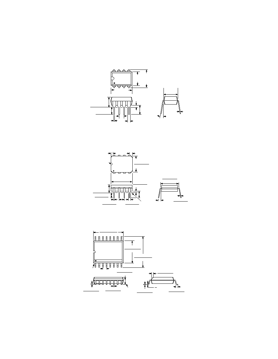
OUTLINE DIMENSIONS
Dimensions shown in inches and (mm).
Plastic
Mini-DIP (N)
Package
0.035
0.01
(0.89
0.25)
0.165
0.01
(4.19 0.25)
0.018
0.003
0.46
0.08
0.125 (3.18)
MIN
0.18
0.03
(4.57
0.76)
0.39 (9.91)
MAX
0.25
(6.35)
0.011
0.003
(0.28
0.08)
0.30 (7.62)
REF
0.31
(7.87)
SEATING
PLANE
0.033 (0.84)
NOM
0-15
0.10
(2.54)
TYP
8
1
4
5
Cerdip (Q) Package
8
1
4
5
0.005 (0.13)
MIN
0.055 (1.4)
MAX
SEATING
PLANE
0.014 (0.36)
0.023 (0.58)
0.20 (5.08)
MAX
0.150
(3.81)
MIN
0.03 (1.76)
0.07 (0.78)
0.125 (3.18)
0.200 (5.08)
0.1
(2.54)
BSC
0.015 (0.38)
0.06 (1.52)
0.405 (10.29)
MAX
0∞-15∞
0.220 (5.59)
0.310 (7.87)
0.008 (0.20)
0.015 (0.38)
0.25 (0.64)
0.290 (7.37)
0.320 (8.13)
R-16 Package
SEATING
PLANE
0.0118 (0.30)
0.0040 (0.10)
0.0192 (0.49)
0.0138 (0.35)
0.1043 (2.65)
0.0926 (2.35)
0.050 (1.27)
BSC
16
9
8
1
0.4193 (10.65)
0.3937 (10.00)
0.2992 (7.60)
0.2914 (7.40)
PIN 1
0.4133 (10.50)
0.3977 (10.00)
0.0125 (0.32)
0.0091 (0.23)
8
0
0.0291 (0.74)
0.0098 (0.25)
45
0.0500 (1.27)
0.0157 (0.40)