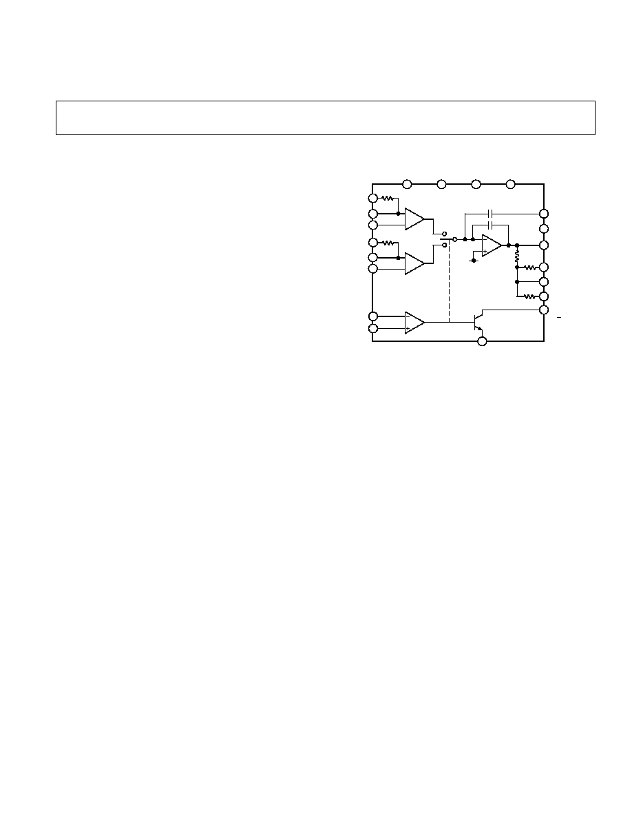
FUNCTIONAL BLOCK DIAGRAM
CM OFF
ADJ
CM OFF
ADJ
DIFF OFF
ADJ
DIFF OFF
ADJ
6
3
4
5
2.5k
AMP A
2.5k
AMP B
≠V
10k
10k
17
5k
8
9
10
COMP
19
18
1
15
7
16
14
13
11
12
R
IN
A
CHA+
CHA≠
R
IN
B
CHB+
CHB≠
SEL B
SEL A
2
20
COMP
+V
S
V
OUT
R
B
R
F
R
A
CHANNEL
STATUS
B/A
≠V
S
AD630
A
B
REV. C
Information furnished by Analog Devices is believed to be accurate and
reliable. However, no responsibility is assumed by Analog Devices for its
use, nor for any infringements of patents or other rights of third parties
which may result from its use. No license is granted by implication or
otherwise under any patent or patent rights of Analog Devices.
a
Balanced Modulator/Demodulator
AD630
PRODUCT DESCRIPTION
The AD630 is a high precision balanced modulator which com-
bines a flexible commutating architecture with the accuracy and
temperature stability afforded by laser wafer trimmed thin-film
resistors. Its signal processing applications include balanced
modulation and demodulation, synchronous detection, phase
detection, quadrature detection, phase sensitive detection,
lock-in amplification and square wave multiplication. A network
of on-board applications resistors provides precision closed loop
gains of
±1 and ±2 with 0.05% accuracy (AD630B). These
resistors may also be used to accurately configure multiplexer
gains of +1, +2, +3 or +4. Alternatively, external feedback may
be employed allowing the designer to implement his own high
gain or complex switched feedback topologies.
The AD630 may be thought of as a precision op amp with two
independent differential input stages and a precision comparator
which is used to select the active front end. The rapid response
time of this comparator coupled with the high slew rate and fast
settling of the linear amplifiers minimize switching distortion. In
addition, the AD630 has extremely low crosstalk between chan-
nels of ≠100 dB @ 10 kHz.
The AD630 is intended for use in precision signal processing
and instrumentation applications requiring wide dynamic range.
When used as a synchronous demodulator in a lock-in amplifier
configuration, it can recover a small signal from 100 dB of inter-
fering noise (see lock-in amplifier application). Although optimized
for operation up to 1 kHz, the circuit is useful at frequencies up
to several hundred kilohertz.
Other features of the AD630 include pin programmable frequency
compensation, optional input bias current compensation resis-
tors, common-mode and differential-offset voltage adjustment,
and a channel status output which indicates which of the two
differential inputs is active. This device is now available to Stan-
dard Military Drawing (DESC) numbers 5962-8980701RA and
5962-89807012A.
PRODUCT HIGHLIGHTS
1. The configuration of the AD630 makes it ideal for signal
processing applications such as: balanced modulation and
demodulation, lock-in amplification, phase detection, and
square wave multiplication.
2. The application flexibility of the AD630 makes it the best
choice for many applications requiring precisely fixed gain,
switched gain, multiplexing, integrating-switching functions,
and high-speed precision amplification.
3. The 100 dB dynamic range of the AD630 exceeds that of any
hybrid or IC balanced modulator/demodulator and is compa-
rable to that of costly signal processing instruments.
4. The op-amp format of the AD630 ensures easy implementa-
tion of high gain or complex switched feedback functions.
The application resistors facilitate the implementation of
most common applications with no additional parts.
5. The AD630 can be used as a two channel multiplexer with
gains of +1, +2, +3 or +4. The channel separation of
100 dB @ 10 kHz approaches the limit which is achievable
with an empty IC package.
6. The AD630 has pin-strappable frequency compensation (no
external capacitor required) for stable operation at unity gain
without sacrificing dynamic performance at higher gains.
7. Laser trimming of comparator and amplifying channel offsets
eliminates the need for external nulling in most cases.
FEATURES
Recovers Signal from +100 dB Noise
2 MHz Channel Bandwidth
45 V/ s Slew Rate
≠120 dB Crosstalk @ 1 kHz
Pin Programmable Closed Loop Gains of 1 and 2
0.05% Closed Loop Gain Accuracy and Match
100 V Channel Offset Voltage (AD630BD)
350 kHz Full Power Bandwidth
Chips Available
One Technology Way, P.O. Box 9106, Norwood, MA 02062-9106, U.S.A.
Tel: 781/329-4700
World Wide Web Site: http://www.analog.com
Fax: 781/326-8703
© Analog Devices, Inc., 2000

AD630≠SPECIFICATIONS
REV. C
≠2≠
ORDERING GUIDE
Temperature
Package
Package
Model
Ranges
Descriptions
Options
AD630JN
0
∞C to +70∞C
Plastic DIP
N-20
AD630KN
0
∞C to +70∞C
Plastic DIP
N-20
AD630AD
≠25
∞C to +85∞C Side Brazed DIP D-20
AD630BD
≠25
∞C to +85∞C Side Brazed DIP D-20
AD630SD
≠55
∞C to +125∞C Side Brazed DIP D-20
AD630SD/883B
≠55
∞C to +125∞C Side Brazed DIP D-20
5962-8980701RA ≠55
∞C to +125∞C Side Brazed DIP D-20
AD630SE/883B
≠55
∞C to +125∞C LCC
E-20A
5962-89807012A ≠55
∞C to +125∞C LCC
E-20A
AD630JCHIPS
0
∞C to +70∞C
Chip
AD630SCHIPS
≠55
∞C to +125∞C Chip
(@ + 25 C and V
S
= 15 V unless otherwise noted)
Model
AD630J/A
AD630K/B
AD630S
Min
Typ
Max
Min
Typ
Max
Min
Typ
Max
Unit
GAIN
Open Loop Gain
90
110
100
120
90
110
dB
±1, ±2 Closed Loop Gain Error
0.1
0.05
0.1
%
Closed Loop Gain Match
0.1
0.05
0.1
%
Closed Loop Gain Drift
2
2
2
ppm/
∞C
CHANNEL INPUTS
V
IN
Operational Limit
1
(≠V
S
+ 4 V) to (+V
S
≠ 1 V)
(≠V
S
+ 4 V) to (+V
S
≠ 1 V)
(≠V
S
+ 4 V) to (+V
S
≠ 1 V)
Volts
Input Offset Voltage
500
100
500
µV
Input Offset Voltage
T
MIN
to T
MAX
800
160
1000
µV
Input Bias Current
100
300
100
300
100
300
nA
Input Offset Current
10
50
10
50
10
50
nA
Channel Separation @ 10 kHz
100
100
100
dB
COMPARATOR
V
IN
Operational Limit
1
(≠V
S
+ 3 V) to (+V
S
≠ 1.5 V)
(≠V
S
+ 3 V) to (+V
S
≠ 1.5 V)
(≠V
S
+ 3 V) to (+V
S
≠ 1.3 V)
Volts
Switching Window
1.5
1.5
1.5
mV
Switching Window
T
MIN
to T
MAX
2
2.0
2.0
2.5
mV
Input Bias Current
100
300
100
300
100
300
nA
Response Time (≠5 mV to +5 mV Step)
200
200
200
ns
Channel Status
I
SINK
@ V
OL
= ≠V
S
+ 0.4 V
3
1.6
1.6
1.6
mA
Pull-Up Voltage
(≠V
S
+ 33 V)
(≠V
S
+ 33 V)
(≠V
S
+ 33 V)
Volts
DYNAMIC PERFORMANCE
Unity Gain Bandwidth
2
2
2
MHz
Slew Rate
4
45
45
45
V/
µs
Settling Time to 0.1% (20 V Step)
3
3
3
µs
OPERATING CHARACTERISTICS
Common-Mode Rejection
85
105
90
110
90
110
dB
Power Supply Rejection
90
110
90
110
90
110
dB
Supply Voltage Range
5
±16.5
5
±16.5
5
±16.5
Volts
Supply Current
4
5
4
5
4
5
mA
OUTPUT VOLTAGE, @ R
L
= 2 k
T
MIN
to T
MAX
2
10
10
±10
Volts
Output Short Circuit Current
25
25
25
mA
TEMPERATURE RANGES
Rated Performance≠N Package
0
+70
0
+70
N/A
∞C
Rated Performance≠
D Package
≠25
+85
≠25
+85
≠55
+125
∞C
NOTES
1
If one terminal of each differential channel or comparator input is kept within these limits the other terminal may be taken to the positive supply.
2
These parameters are guaranteed but not tested for J and K grades. For A, B and S grades they are tested.
3
I
SINK
@ V
OL
= (≠V
S
+ 1) volt is typically 4 mA.
4
Pin 12 Open. Slew rate with Pins 12 and 13 shorted is typically 35 V/
µs.
Specifications subject to change without notice.
Specifications shown in boldface are tested on all production units at final electrical test. Results from those tests are used to calculate outgoing quality levels. All min
and max specifications are guaranteed, although only those shown in boldface are tested on all production units.
ABSOLUTE MAXIMUM RATINGS
Supply Voltage . . . . . . . . . . . . . . . . . . . . . . . . . . . . . . . . .
±18 V
Internal Power Dissipation . . . . . . . . . . . . . . . . . . . . . 600 mW
Output Short Circuit to Ground . . . . . . . . . . . . . . . . Indefinite
Storage Temperature, Ceramic Package . . . . ≠65
∞C to +150∞C
Storage Temperature, Plastic Package . . . . . . ≠55
∞C to +125∞C
Lead Temperature Range (Soldering, 10 sec ) . . . . . . . +300
∞C
Max Junction Temperature . . . . . . . . . . . . . . . . . . . . . +150
∞C
THERMAL CHARACTERISTICS
JC
JA
20-Pin Plastic DIP (N)
24
∞C/W
61
∞C/W
20-Pin Ceramic DIP (D)
35
∞C/W
120
∞C/W
20-Pin Leadless Chip Carrier (E)
35
∞C/W
120
∞C/W
AD630
REV. C
≠3≠
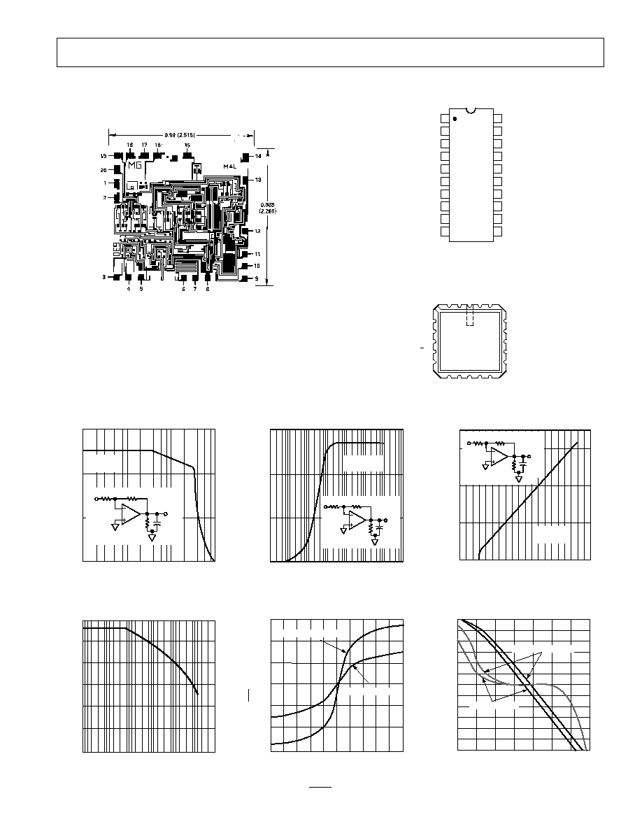
PIN CONFIGURATIONS
20-Lead DIP (D-20 and N-20)
14
13
12
11
17
16
15
20
19
18
10
9
8
1
2
3
4
7
6
5
TOP VIEW
(Not to Scale)
AD630
R
IN
A
R
IN
B
CH B+
CH B≠
CH A≠
CH A+
DIFF OFF ADJ
DIFF OFF ADJ
R
B
R
F
R
A
CM OFF ADJ
CM OFF ADJ
≠V
S
SEL B
SEL A
+V
S
COMP
V
OUT
CHANNEL STATUS B/
A
20-Contact LCC (E-20A)
20 19
1
2
3
18
14
15
16
17
4
5
6
7
8
9 10 11 12 13
TOP VIEW
(Not to Scale)
AD630
DIFF OFF ADJ
CM OFF ADJ
CM OFF ADJ
CHANNEL STATUS B/A
≠V
S
CH B+
R
IN
B
R
A
R
F
R
B
DIFF
OFF ADJ
CH A+
R
IN
A
CH A
≠
CH B
≠
SEL B
SEL A
+V
S
COMP
V
OUT
Typical Performance Characteristics
Figure 2. Output Voltage vs.
Resistive Load
Figure 3. Output Voltage Swing
vs. Supply Voltage
Figure 4. Common-Mode
Rejection vs. Frequency
Figure 5.
dV
O
dt
vs. Input Voltage
Figure 6. Gain and Phase vs.
Frequency
CHIP METALIZATION AND PINOUT
Dimensions shown in inches and (mm).
Contact factory for latest dimensions
CHIP AVAILABILITY
The AD630 is available in laser trimmed, passivated chip form.
The figure shows the AD630 metalization pattern, bonding pads
and dimensions. AD630 chips are available; consult factory for
details.
Figure 1. Output Voltage vs.
Frequency
FREQUENCY ≠ Hz
15
10
5
1k
10k
1M
100k
R
L
=
2k
C
L
= 100pF
2k
5k
5k
V
i
V
O
100pF
OUTPUT VOLTAGE
≠
V
10
15
5
1
10
100
1k
10k
100k
1M
RESISTIVE LOAD ≠
C
L
= 100pF
f = 1kHz
CAP IN
5k
V
O
100pF
R
L
V
i
5k
OUTPUT VOLTAGE
≠
V
10
18
5
0
5
10
15
SUPPLY VOLTAGE ≠ V
OUTPUT VOLTAGE
≠
V
15
5k
100pF
V
i
5k
2k
V
O
f = 1kHz
C
L
= 100pF
FREQUENCY ≠ Hz
COMMON MODE REJECTION
≠
dB
120
60
0
1
10
100k
100
1k
10k
100
80
40
20
INPUT VOLTAGE ≠ V
DV
O
dt
≠
V/
s
60
0
≠60
≠5
≠3
4
≠2
≠1
1
40
20
≠40
≠20
≠4
0
2
3
5
UNCOMPENSATED
COMPENSATED
FREQUENCY ≠ Hz
120
60
0
1M
100
100
80
20
40
10
1k
100k
10k
UNCOMPENSATED
10M
0
45
90
OPEN LOOP GAIN
≠
dB
135
180
COMPENSATED
OPEN LOOP PHASE
≠
Degrees
REV. C
≠4≠
AD630≠Typical Performance Characteristics
Figure 7. Channel-to-Channel Switch-
Settling Characteristic
Figure 9. Large Signal Inverting
Step Response
TWO WAYS TO LOOK AT THE AD630
The functional block diagram of the AD630 (see page 1) also
shows the pin connections of the internal functions. An alternative
architectural diagram is shown in Figure 10. In this diagram, the
individual A and B channel preamps, the switch, and the inte-
grator output amplifier are combined in a single op amp. This
amplifier has two differential input channels, only one of which
is active at a time.
11
15
2
20
19
18
17
8
7
12
14
13
9
10
R
A
5k
2.5k
R
F
10k
1
16
2.5k
+V
S
R
B
10k
SEL B
SEL A
B/A
A
B
≠V
S
Figure 10. Architectural Block Diagram
HOW THE AD630 WORKS
The basic mode of operation of the AD630 may be more easy to
recognize as two fixed gain stages which may be inserted into the
signal path under the control of a sensitive voltage comparator.
When the circuit is switched between inverting and noninverting
gain, it provides the basic modulation/demodulation function. The
AD630 is unique in that it includes Laser-Wafer-Trimmed thin-
film feedback resistors on the monolithic chip. The configuration
shown in Figure 11 yields a gain of
±2 and can be easily changed to
±1 by shifting R
B
from its ground connection to the output.
The comparator selects one of the two input stages to complete
an operational feedback connection around the AD630. The
deselected input is off and has negligible effect on the operation.
A
B
R
A
5k
R
F
10k
V
O
R
B
10k
V
i
2
20
19
18
13
15
16
14
9
10
Figure 11. AD630 Symmetric Gain (
±2)
When channel B is selected, the resistors R
A
and R
F
are con-
nected for inverting feedback as shown in the inverting gain
configuration diagram in Figure 12. The amplifier has sufficient
loop gain to minimize the loading effect of R
B
at the virtual
ground produced by the feedback connection. When the sign of
the comparator input is reversed, input B will be deselected and
A will be selected. The new equivalent circuit will be the nonin-
verting gain configuration shown below. In this case R
A
will appear
across the op-amp input terminals, but since the amplifier drives
this difference voltage to zero the closed loop gain is unaffected.
The two closed loop gain magnitudes will be equal when R
F
/R
A
= 1 + R
F
/R
B
, which will result from making R
A
equal to R
F
R
B
/
(R
F
+ R
B
) the parallel equivalent resistance of R
F
and R
B
.
The 5k and the two 10k resistors on the AD630 chip can be
used to make a gain of two as shown here. By paralleling the
10k resistors to make R
F
equal 5k and omitting R
B
the circuit
can be programmed for a gain of
±1 (as shown in Figure 18a).
These and other configurations using the on chip resistors
present the inverting inputs with a 2.5k source impedance. The
more complete AD630 diagrams show 2.5k resistors available at
the noninverting inputs which can be conveniently used to mini-
mize errors resulting from input bias currents.
Figure 8. Small Signal Noninverting
Step Response
20mV
500ns
20mV
100
90
10
0%
20mV/DIV
(V
o
)
20mV/DIV
(V
i
)
TOP TRACE: Vo
BOTTOM TRACE: Vi
100
90
10
0%
100mV
500ns
50mV
1mV
50mV/DIV
(V
i
)
1mV/DIV
(A)
TOP TRACE: Vi
MIDDLE TRACE: SETTLING
ERROR (A)
BOTTOM TRACE: Vo
100mV/DIV
(V
o
)
100
90
10
0%
10V
10V
1mV
TOP TRACE: Vi
MIDDLE TRACE: SETTLING
ERROR (B)
BOTTOM TRACE: Vo
5 s
10V 20kHz
(V
i
)
1mV/DIV
(B)
10V/DIV
(V
o
)
5k
10k
10k
V
i
CH
A
CH
B
12
V
O
2
20
19
18
13
9
10
14
16
15
12
CH A
MIDDLE
TRACE
(A)
10k
10k
V
O
BOTTOM
TRACE
TEKTRONIX
7A13
10k
1k
30pF
10k
V
i
TOP
TRACE
2
20
13
14
15
12
CH A
10k
10k
V
O
BOTTOM
TRACE
10k
V
i
TOP
TRACE
(B)
MIDDLE
TRACE
10k
HP5082-2811
20
2
13
14
15
AD630
REV. C
≠5≠
R
A
5k
R
F
10k
R
B
10k
V
i
V
O
= ≠
R
F
R
A
V
i
Figure 12. Inverting Gain Configuration
R
A
5k
R
F
10k
R
B
10k
V
i
V
O
=
(
1+
R
F
R
B
)
V
i
Figure 13. Noninverting Gain Configuration
CIRCUIT DESCRIPTION
The simplified schematic of the AD630 is shown in Figure 14.
It has been subdivided into three major sections, the comparator,
the two input stages and the output integrator. The comparator
consists of a front end made up of Q52 and Q53, a flip-flop load
formed by Q3 and Q4, and two current steering switching cells
Q28, Q29 and Q30, Q31. This structure is designed so that a
differential input voltage greater than 1.5 mV in magnitude
applied to the comparator inputs will completely select one the
switching cells. The sign of this input voltage determine which
of the two switching cells is selected.
20
11
3
4
5
6
19
2
18
13
12
SEL A
SEL B
DIFF
OFF ADJ
DIFF
OFF ADJ
CM
OFF ADJ
CM
OFF ADJ
COMP
Q74
Q44
CH B≠
CH B+
CH A+
CH A≠
i55
Q4
Q3
Q28
Q31
Q30
Q32
C122
C121
i22
i23
≠V
S
V
O
i73
Q52
Q53
+V
S
Q65
Q34
Q33
Q62
Q35
Q36
Q67
Q70
Q25
Q24
Q29
10
9
8
Figure 14. AD630 Simplified Schematic
The collectors of each switching cell connect to an input trans-
conductance stage. The selected cell conveys bias currents i
22
and i
23
to the input stage it controls, causing it to become active.
The deselected cell blocks the bias to its input stage which, as a
consequence, remains off.
The structure of the transconductance stages is such that they
present a high impedance at their input terminals and draw no
bias current when deselected. The deselected input does not
interfere with the operation of the selected input insuring maxi-
mum channel separation.
Another feature of the input structure is that it enhances the
slew rate of the circuit. The current output of the active stage
follows a quasi-hyperbolic-sine relationship to the differential
input voltage. This means that the greater the input voltage, the
harder this stage will drive the output integrator, and hence, the
faster the output signal will move. This feature helps insure
rapid, symmetric settling when switching between inverting and
noninverting closed loop configurations.
The output section of the AD630 includes a current mirror-load
(Q24 and Q25), an integrator-voltage gain stage (Q32), and
complementary output buffer (Q44 and Q74). The outputs of
both transconductance stages are connected in parallel to the
current mirror. Since the deselected input stage produces no
output current and presents a high impedance at its outputs,
there is no conflict. The current mirror translates the differential
output current from the active input transconductance amplifier
into single ended form for the output integrator. The comple-
mentary output driver then buffers the integrator output pro-
duce a low impedance output.
OTHER GAIN CONFIGURATIONS
Many applications require switched gains other than the
±1 and
±2 which the self-contained applications resistors provide. The
AD630 can be readily programmed with three external resistors
over a wide range of positive and negative gain by selecting and
R
B
and R
F
to give the noninverting gain 1 + R
F
/R
B
and subsequent
R
A
to give the desired inverting gain. Note that when the inverting
magnitude equals the noninverting magnitude, the value of R
A
is
found to be R
B
R
F
/(R
B
+ R
F
). That is, R
A
should equal the parallel
combination of R
B
and R
F
to match positive and negative gain.
The feedback synthesis of the AD630 may also include reactive
impedance. The gain magnitudes will match at all frequencies if
the A impedance is made to equal the parallel combination of
the B and F impedances. Essentially the same considerations
apply to the AD630 as to conventional op-amp feedback circuits.
Virtually any function which can be realized with simple nonin-
verting "L network" feedback can be used with the AD630. A
common arrangement is shown in Figure 15. The low frequency
gain of this circuit is 10. The response will have a pole (≠3 dB)
at a frequency f 1/(2
100 kC) and a zero (3 dB from the
high frequency asymptote) at about 10 times this frequency.
The 2k resistor in series with each capacitor mitigates the load-
ing effect on circuitry driving this circuit, eliminates stability
problems, and has a minor effect on the pole-zero locations.
As a result of the reactive feedback, the high frequency components
of the switched input signal will be transmitted at unity gain
C
≠V
S
A
B
10k
V
O
11.11k
12
V
i
100k
2k
C
2k
2
20
19
18
13
7
8
9
10
Figure 15. AD630 with External Feedback
while the low frequency components will be amplified. This
arrangement is useful in demodulators and lock-in amplifiers. It
increases the circuit dynamic range when the modulation or
interference is substantially larger than the desired signal ampli-
tude. The output signal will contain the desired signal multi-
plied by the low frequency gain (which may be several hundred
for large feedback ratios) with the switching signal and interfer-
ence superimposed at unity gain.