REV. D
Information furnished by Analog Devices is believed to be accurate and
reliable. However, no responsibility is assumed by Analog Devices for its
use, nor for any infringements of patents or other rights of third parties
which may result from its use. No license is granted by implication or
otherwise under any patent or patent rights of Analog Devices.
a
Software Programmable
Gain Amplifier
AD526
FEATURES
Digitally Programmable Binary Gains from 1 to 16
Two-Chip Cascade Mode Achieves Binary Gain from
1 to 256
Gain Error:
0.01% Max, Gain = 1, 2, 4 (C Grade)
0.02% Max, Gain = 8, 16 (C Grade)
0.5 ppm/ C Drift Over Temperature
Fast Settling Time
10 V Signal Change:
0.01% in 4.5 s (Gain = 16)
Gain Change:
0.01% in 5.6 s (Gain = 16)
Low Nonlinearity: 0.005% FSR Max (J Grade)
Excellent DC Accuracy:
Offset Voltage: 0.5 mV Max (C Grade)
Offset Voltage Drift: 3 V/ C (C Grade)
TTL-Compatible Digital Inputs
PRODUCT DESCRIPTION
The AD526 is a single-ended, monolithic software program-
mable gain amplifier (SPGA) that provides gains of 1, 2, 4, 8
and 16. It is complete, including amplifier, resistor network
and TTL-compatible latched inputs, and requires no external
components.
Low gain error and low nonlinearity make the AD526 ideal for
precision instrumentation applications requiring programmable
gain. The small signal bandwidth is 350 kHz at a gain of 16. In
addition, the AD526 provides excellent dc precision. The FET-
input stage results in a low bias current of 50 pA. A guaranteed
maximum input offset voltage of 0.5 mV max (C grade) and low
gain error (0.01%, G = 1, 2, 4, C grade) are accomplished using
Analog Devices' laser trimming technology.
To provide flexibility to the system designer, the AD526 can be
operated in either latched or transparent mode. The force/sense
configuration preserves accuracy when the output is connected
to remote or low impedance loads.
The AD526 is offered in one commercial (0
∞
C to +70
∞
C) grade,
J, and three industrial grades, A, B and C, which are specified
from ≠40
∞
C to +85
∞
C. The S grade is specified from ≠55
∞
C to
+125
∞
C. The military version is available processed to MIL-
STD 883B, Rev C. The J grade is supplied in a 16-lead plastic
DIP, and the other grades are offered in a 16-lead hermetic
side-brazed ceramic DIP.
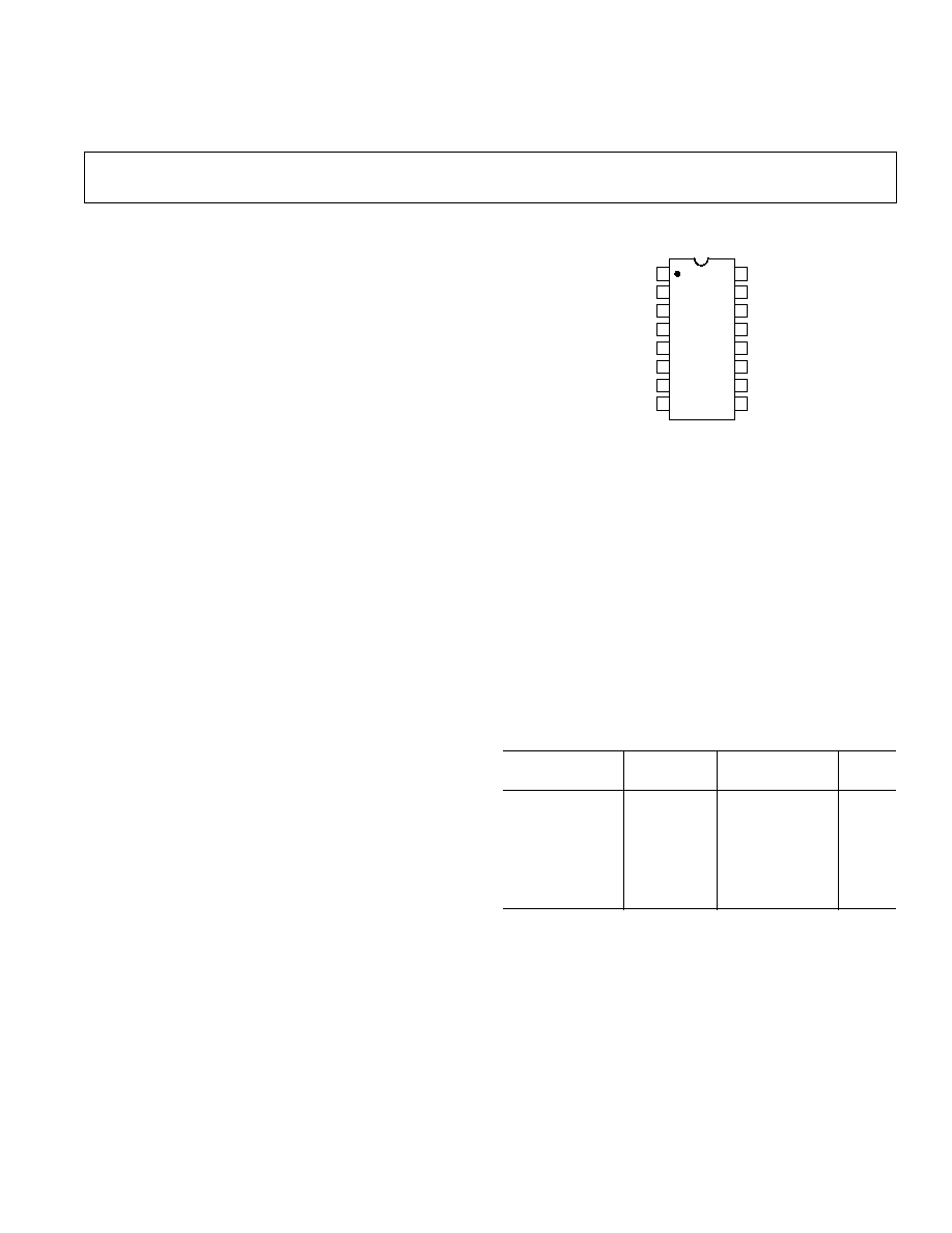
PIN CONFIGURATION
TOP VIEW
(Not to Scale)
16
15
14
13
12
11
10
9
1
2
3
4
5
6
7
8
DIG GND
A1
AD526
NULL
A0
V
IN
CS
NULL
CLK
ANALOG GND 2
A2
ANALOG GND 1
B
≠V
S
+V
S
V
OUT
SENSE
V
OUT
FORCE
One Technology Way, P.O. Box 9106, Norwood, MA 02062-9106, U.S.A.
Tel: 781/329-4700
World Wide Web Site: http://www.analog.com
Fax: 781/326-8703
© Analog Devices, Inc., 1999
ORDERING GUIDE
Temperature
Package
Package
Model
Range
Descriptions
Options
AD526JN
Commercial
16-Lead Plastic DIP N-16
AD526AD
Industrial
16-Lead Cerdip
D-16
AD526BD
Industrial
16-Lead Cerdip
D-16
AD526CD
Industrial
16-Lead Cerdip
D-16
AD526SD
Military
16-Lead Cerdip
D-16
AD526SD/883B
Military
16-Lead Cerdip
D-16
5962-9089401MEA* Military
16-Lead Cerdip
D-16
*Refer to official DESC drawing for tested specifications.
APPLICATION HIGHLIGHTS
1. Dynamic Range Extension for ADC Systems: A single
AD526 in conjunction with a 12-bit ADC can provide
96 dB of dynamic range for ADC systems.
2. Gain Ranging Preamps: The AD526 offers complete digital
gain control with precise gains in binary steps from 1 to 16.
Additional gains of 32, 64, 128 and 256 are possible by cas-
cading two AD526s.

AD526≠Typical Performance Characteristics
REV. D
≠4≠
SUPPLY VOLTAGE ≠ V
OUTPUT VOLTAGE SWING ≠
V
20
15
0
0
5
20
10
15
10
5
+25 C
R
L
= 2k
Figure 1. Output Voltage Swing vs.
Supply Voltage, G = 16
TEMPERATURE ≠ C
INPUT BIAS CURRENT
100nA
10nA
1pA
≠60
≠20
140
20
60
100
1nA
100pA
10pA
Figure 4. Input Bias Current vs.
Temperature
FREQUENCY ≠ Hz
FULL POWER RESPONSE ≠ V p-p
25
1k
GAIN = 8, 16
GAIN = 1, 2, 4
20
15
10
5
0
10k
100k
1M
10M
Figure 7. Large Signal Frequency
Response
LOAD RESISTANCE ≠
OUTPUT VOLTAGE SWING ≠
V
30
0
100
1k
10k
20
10
@ V
S
= 15V
Figure 2. Output Voltage Swing vs.
Load Resistance
INPUT VOLTAGE ≠ V
INPUT BIAS CURRENT ≠ pA
75
≠10
50
25
0
≠5
0
5
10
V
S
= 15V
Figure 5. Input Bias Current vs. Input
Voltage
FREQUENCY ≠ Hz
POWER SUPPLY REJECTION ≠ dB
100
1
80
60
40
20
10
10
100
1k
10k
100k
1M
15V WITH 1V p-p
SINE WAVE
+SUPPLY
≠SUPPLY
Figure 8. PSRR vs. Frequency
SUPPLY VOLTAGE ≠ V
INPUT BIAS CURRENT ≠ pA
20
15
0
0
5
20
10
15
10
5
V
IN
= 0
Figure 3. Input Bias Current vs.
Supply Voltage
FREQUENCY ≠ Hz
GAIN
20
10
100
10M
10
1
1k
10k
100k
1M
16
8
4
2
1
Figure 6. Gain vs. Frequency
TEMPERATURE ≠ C
NORMALIZED GAIN
1.0002
≠60
1.0001
1.0000
0.9999
0.9998
≠20
20
60
100
140
Figure 9. Normalized Gain vs.
Temperature, Gain = 1

AD526
REV. D
≠5≠
*For Settling Time Traces, 0.01% = 1/2 Vertical Division
FREQUENCY ≠ Hz
1000
10
100
INPUT NOISE VOLTAGE ≠ nV/ Hz
10
100k
100
1k
10k
Figure 10. Noise Spectral Density
Figure 13. Large Signal Pulse
Response and Settling Time,*
G = 1
Figure 16. Small Signal Pulse
Response, G = 2
TEMPERATURE ≠ C
NONLINEARITY ≠ %FSR
0.006
≠60
0.004
0.002
0.000
≠0.002
≠0.004
≠20
20
60
100
140
Figure 11. Nonlinearity vs.
Temperature, Gain = 1
Figure 14. Small Signal Pulse
Response, G = 1
Figure 17. Large Signal Pulse
Response and Settling Time,*
G = 4
Figure 12. Wideband Output Noise,
G = 16 (Amplified by 10)
Figure 15. Large Signal Pulse
Response and Settling Time,*
G = 2
Figure 18. Small Signal Pulse
Response, G = 4