
ATN OUT
AMPLIFIER/LIMITER
FULL-WAVE
DETECTOR
ATN LO
ATN COM
SIG +IN
SIG ≠IN
ATN COM
COM
27
30
270
ATN IN
1k
RG1
RG0
RG2
≠V
S
BL1
+V
S
LOG OUT
LOG COM
SIG +OUT
SIG ≠OUT
BL2
ITC
20
1
INTERCEPT POSITIONING BIAS
19
3
2
4
18
5
6
GAIN BIAS REGULATOR
AMPLIFIER/LIMITER
FULL-WAVE
DETECTOR
AMPLIFIER/LIMITER
FULL-WAVE
DETECTOR
10dB
AMPLIFIER/LIMITER
FULL-WAVE
DETECTOR
10dB
10dB
AMPLIFIER/LIMITER
FULL-WAVE
DETECTOR
17
16
14
13
1k
7
11
10
9
8
12
SLOPE BIAS REGULATOR
15
10dB
10dB
a
DC-Coupled Demodulating
120 MHz Logarithmic Amplifier
AD640*
One Technology Way, P.O. Box 9106, Norwood, MA 02062-9106, U.S.A.
Tel: 781/329-4700
World Wide Web Site: http://www.analog.com
Fax: 781/326-8703
© Analog Devices, Inc., 1999
FEATURES
Complete, Fully Calibrated Monolithic System
Five Stages, Each Having 10 dB Gain, 350 MHz BW
Direct Coupled Fully Differential Signal Path
Logarithmic Slope, Intercept and AC Response are
Stable Over Full Military Temperature Range
Dual Polarity Current Outputs Scaled 1 mA/Decade
Voltage Slope Options (1 V/Decade, 100 mV/dB, etc.)
Low Power Operation (Typically 220 mW at 5 V)
Low Cost Plastic Packages Also Available
APPLICATIONS
Radar, Sonar, Ultrasonic and Audio Systems
Precision Instrumentation from DC to 120 MHz
Power Measurement with Absolute Calibration
Wide Range High Accuracy Signal Compression
Alternative to Discrete and Hybrid IF Strips
Replaces Several Discrete Log Amp ICs
PRODUCT DESCRIPTION
The AD640 is a complete monolithic logarithmic amplifier. A single
AD640 provides up to 50 dB of dynamic range for frequencies
from dc to 120 MHz. Two AD640s in cascade can provide up to
95 dB of dynamic range at reduced bandwidth. The AD640 uses a
successive detection scheme to provide an output current propor-
tional to the logarithm of the input voltage. It is laser calibrated to
close tolerances and maintains high accuracy over the full military
temperature range using supply voltages from
±
4.5 V to
±
7.5 V.
The AD640 comprises five cascaded dc-coupled amplifier/limiter
stages, each having a small signal voltage gain of 10 dB and a ≠3 dB
bandwidth of 350 MHz. Each stage has an associated full-wave
detector, whose output current depends on the absolute value of its
input voltage. The five outputs are summed to provide the video
output (when low-pass filtered) scaled at 1 mA per decade (50
µ
A
per dB). On chip resistors can be used to convert this output cur-
rent to a voltage with several convenient slope options. A balanced
signal output at +50 dB (referred to input) is provided to operate
AD640s in cascade.
The logarithmic response is absolutely calibrated to within
±
1 dB
for dc or square wave inputs from
±
0.75 mV to
±
200 mV, with
an intercept (logarithmic offset) at 1 mV dc. An integral X10
attenuator provides an alternative input range of
±
7.5 mV to
±
2 V dc. Scaling is also guaranteed for sinusoidal inputs.
The AD640B is specified for the industrial temperature range of
≠40
∞
C to +85
∞
C and the AD640T, available processed to MIL-
STD-883B, for the military range of ≠55
∞
C to +125
∞
C. Both are
available in 20-lead side-brazed ceramic DIPs or leadless chip
carriers (LCC). The AD640J is specified for the commercial
temperature range of 0
∞
C to +70
∞
C, and is available in both
20-lead plastic DIP (N) and PLCC (P) packages.
This device is now available to Standard Military Drawing
(DESC) number 5962-9095501MRA and 5962-9095501M2A.
PRODUCT HIGHLIGHTS
1. Absolute calibration of a wideband logarithmic amplifier is
unique. The AD640 is a high accuracy measurement device,
not simply a logarithmic building block.
2. Advanced design results in unprecedented stability over the
full military temperature range.
3. The fully differential signal path greatly reduces the risk of
instability due to inadequate power supply decoupling and
shared ground connections, a serious problem with com-
monly used unbalanced designs.
4. Differential interfaces also ensure that the appropriate ground
connection can be chosen for each signal port. They further
increase versatility and simplify applications. The signal input
impedance is ~500 k
in shunt with ~2 pF.
5. The dc-coupled signal path eliminates the need for numerous
interstage coupling capacitors and simplifies logarithmic
conversion of subsonic signals.
(continued on page 4)
FUNCTIONAL BLOCK DIAGRAM
REV. C
Information furnished by Analog Devices is believed to be accurate and
reliable. However, no responsibility is assumed by Analog Devices for its
use, nor for any infringements of patents or other rights of third parties
which may result from its use. No license is granted by implication or
otherwise under any patent or patent rights of Analog Devices.
*Protected under U.S. patent number 4,990,803.

AD640≠SPECIFICATIONS
DC SPECIFICATIONS
Model
AD640J
AD640B
AD640T
Parameter
Conditions
Min
Typ
Max
Min
Typ
Max
Min
Typ
Max
Units
TRANSFER FUNCTION
1
I
OUT
= I
Y
LOG |V
IN
/V
X
| for V
IN
=
±
0.75 mV to
±
200 mV dc
SIGNAL INPUTS (Pins 1, 20)
Input Resistance
Differential
500
500
500
k
Input Offset Voltage
Differential
50
500
50
200
50
200
µ
V
vs. Temperature
0.8
0.8
0.8
µ
V/
∞
C
Over Temperature
T
MIN
to T
MAX
300
µ
V
vs. Supply
2
2
2
µ
V/V
Input Bias Current
7
25
7
25
7
25
µ
A
Input Bias Offset
1
1
1
µ
A
Common-Mode Range
≠2
+0.3
≠2
+0.3
≠2
+0.3
V
INPUT ATTENUATOR
(Pins 2, 3, 4, 5 and 19)
Attenuation
2
Pin 5 to Pin 19
20
20
20
dB
Input Resistance
Pins 5 to 3/4
300
300
300
SIGNAL OUTPUT (Pins 10, 11)
Small Signal Gain
3
50
50
50
dB
Peak Differential Output
4
±
180
±
180
±
180
mV
Output Resistance
Either Pin to COM
75
75
75
Quiescent Output Voltage
Either Pin to COM
≠90
≠90
≠90
mV
LOGARITHMIC OUTPUT
5
(Pin 14)
Voltage Compliance Range
≠0.3
+V
S
≠1
≠0.3
+V
S
≠1
≠0.3
V
S
≠1
V
Slope Current, I
Y
0.95
1.00
1.05
0.98
1.00
1.02
0.98
1.00
1.02
mA
Accuracy vs. Temperature
0.002
0.002
0.002
%/
∞
C
T
MIN
to T
MAX
0.98
1.02
mA
Accuracy vs. Supply
+V
S
= 4.5 V to 7.5 V
0.08
1.0
0.08
0.4
0.08
0.4
%/V
Intercept Voltage
6
, V
X
0.85
1.00
1.15
0.95
1.00
1.05
0.95
1.00
1.05
mV
vs. Temperature
0.5
0.5
0.5
µ
V/
∞
C
Over Temperature
T
MIN
to T
MAX
0.90
1.10
mV
vs. Supply
±
V
S
= 4.5 V to 7.5 V
2
2
2
µ
V/V
Logarithmic Offset
(Alt. Definition of V
X
)
≠61.5
≠60.0
≠58.7
≠60.5
≠60.0
≠59.5
≠60.5
≠60.0
≠59.5
dBV
vs. Temperature
0.004
0.004
0.004
dB/
∞
C
Over Temperature
T
MIN
to T
MAX
≠60.9
≠59.1
dB
vs. Supply
±
V
S
= 4.5 V to 7.5 V
0.017
0.017
0.017
dB/V
Intercept Voltage Using Attenuator
8.25
10.0
11.75
9.0
10.0
11.0
9.0
10.0
11.0
mV
Zero Signal Output Current
7
≠0.2
≠0.2
≠0.2
mA
ITC Disabled
Pin 8 to COM
≠0.27
≠0.27
≠0.27
mA
Maximum Output Current
2.3
2.3
2.3
mA
APPLICATIONS RESISTORS
(Pins 15, 16, 17)
1.000
0.995
1.000
1.005
0.995
1.000
1.005
k
DC LINEARITY
V
IN
±
1 mV to
±
100 mV
0.35
1.2
0.35
0.6
0.35
0.6
dB
TOTAL ABSOLUTE DC
ACCURACY
V
IN
=
±
1 mV to
±
100 mV
8
0.55
2
0.55
0.9
0.55
0.9
dB
Over Temperature
T
MIN
to T
MAX
3
1.7
1.8
dB
Over Supply Range
±
V
S
= 4.5 V to 7.5 V
2
1.0
1.0
dB
V
IN
=
±
0.75 mV to
±
200 mV
1.0
3
1.0
2.0
1.0
2.0
dB
Using Attenuator
V
IN
=
±
10 mV to
±
1 V
0.4
2.5
0.4
1.5
0.4
1.5
dB
Over Temperature
T
MIN
to T
MAX
0.6
3
0.6
2.0
0.6
2.0
dB
V
IN
=
±
7.5 mV to 2 V
1.2
3.5
1.2
2.5
1.2
2.5
dB
POWER REQUIREMENTS
Voltage Supply Range
4.5
7.5
4.5
7.5
4.5
7.5
V
Quiescent Current
9
+V
S
(Pin 12)
T
MIN
to T
MAX
9
15
9
15
9
15
mA
≠V
S
(Pin 7)
T
MIN
to T
MAX
35
60
35
60
35
60
mA
≠2≠
REV. C
(V
S
= 5 V, T
A
= +25 C, unless otherwise noted)

AC SPECIFICATIONS
Model
AD640J
AD640B
AD640T
Parameter
Conditions
Min
Typ
Max
Min
Typ
Max
Min
Typ
Max
Units
SIGNAL INPUTS (Pins 1, 20)
Input Capacitance
Either Pin to COM
2
2
2
pF
Noise Spectral Density
1 kHz to 10 MHz
2
2
2
nV/
Hz
Tangential Sensitivity
BW = 100 MHz
≠72
≠72
≠72
dBm
3 dB BANDWIDTH
Each Stage
350
350
350
MHz
All Five Stages
Pins 1 & 20 to 10 & 11
145
145
145
MHz
LOGARITHMIC OUTPUTS
5
Slope Current, I
Y
f< = 1 MHz
0.96
1.0
1.04
0.98
1.0
1.02
0.98
1.0
1.02
mA
f = 30 MHz
0.88
0.94
1.00
0.91
0.94
0.97
0.91
0.94
0.97
mA
f = 60 MHz
0.82
0.90
0.98
0.86
0.90
0.94
0.86
0.90
0.94
mA
f = 90 MHz
0.88
0.88
0.88
mA
f = 120 MHz
0.85
0.85
0.85
mA
Intercept, Dual AD640s
10, 11
f< = 1 MHz
≠90.6
≠88.6
≠86.6
≠89.6
≠88.6
≠87.6
≠89.6
≠88.6
≠87.6
dBm
f = 30 MHz
≠87.6
≠87.6
≠87.6
dBm
f = 60 MHz
≠86.3
≠86.3
≠86.3
dBm
f = 90 MHz
≠83.9
≠83.9
≠83.9
dBm
f = 120 MHz
≠80.3
≠80.3
≠80.3
dBm
AC LINEARITY
≠40 dBm to ≠2 dBm
12
f = 1 MHz
0.5
2.0
0.5
1.0
0.5
1.0
dB
≠35 dBm to ≠10 dBm
12
f = 1 MHz
0.25
1.0
0.25
0.5
0.25
0.5
dB
≠75 dBm to 0 dBm
10
f = 1 MHz
0.75
3.0
0.75
1.5
0.75
1.5
dB
≠70 dBm to ≠10 dBm
10
f = 1 MHz
0.5
2.0
0.5
1.0
0.5
1.0
dB
≠75 dBm to +15 dBm
13
f = 10 kHz
0.5
3.0
0.5
1.5
0.5
1.5
dB
PACKAGE OPTION
20-Lead Ceramic DIP Package (D)
AD640BD
AD640TD
20-Terminal Ceramic LCC (E)
AD640BE
AD640TE
20-Lead Plastic DIP Package (N)
AD640]N
20-Lead Plastic Leaded Chip Carrier (P)
AD640JP
AD640BP
NUMBER OF TRANSISTORS
155
155
155
NOTES
1
Logarithms to base 10 are used throughout. The response is independent of the sign of V
IN
.
2
Attenuation ratio trimmed to calibrate intercept to 10 mV when in use. It has a temperature coefficient of +0.30%/
∞
C.
3
Overall gain is trimmed using a
±
200
µ
V square wave at 2 kHz, corrected for the onset of compression.
4
The fully limited signal output will appear to be a square wave; its amplitude is proportional to absolute temperature.
5
Currents defined as flowing into Pin 14. See FUNDAMENTALS OF LOGARITHMIC CONVERSION for full explanation of scaling concepts. Slope is measured
by linear regression over central region of transfer function.
6
The logarithmic intercept in dBV (decibels relative to 1 V) is defined as 20 LOG
10
(V
X
/1 V).
7
The zero-signal current is a function of temperature unless internal temperature compensation (ITC) pin is grounded.
8
Operating in circuit of Figure 24 using
±
0.1% accurate values for R
LA
and R
LB.
Includes slope and nonlinearity errors. Input offset errors also included for
V
IN
>3 mV dc, and over the full input range in ac applications.
9
Essentially independent of supply voltages.
10
Using the circuit of Figure 27, using cascaded AD640s and offset nulling. Input is sinusoidal, 0 dBm in 50
= 223 mV rms.
11
For a sinusoidal signal (see EFFECT OF WAVEFORM ON INTERCEPT). Pin 8 on second AD640 must be grounded to ensure temperature stability of intercept
for dual AD640 system.
12
Using the circuit of Figure 24, using single AD640 and offset nulling. Input is sinusoidal, 0 dBm in 50
= 223 mV rms.
13
Using the circuit of Figure 32, using cascaded AD640s and attenuator. Square wave input.
All min and max specifications are guaranteed, but only those in boldface are 100% tested on all production units. Results from those tests are used to calculate
outgoing quality levels.
Specifications subject to change without notice.
THERMAL CHARACTERISTICS
JC
( C/W)
JA
( C/W)
20-Lead Ceramic DIP Package (D-20)
25
85
20-Terminal Ceramic LCC (E-20A)
25
85
20-Lead Plastic DIP Package (N-20)
24
61
20-Lead Plastic Leaded Chip Carrier (P-20A)
28
75
AD640
REV. C
≠3≠
(V
S
= 5 V, T
A
= +25 C, unless otherwise noted)

AD640
REV. C
≠4≠
CHIP DIMENSIONS AND
BONDING DIAGRAM
Dimensions shown in inches and (mm).
ABSOLUTE MAXIMUM RATINGS*
Supply Voltage . . . . . . . . . . . . . . . . . . . . . . . . . . . . . . . .
±
7.5 V
Input Voltage (Pin 1 or Pin 20 to COM) . . . . ≠3 V to +300 mV
Attenuator Input Voltage (Pin 5 to Pin 3/4) . . . . . . . . . . .
±
4 V
Storage Temperature Range D, E . . . . . . . . . ≠65
∞
C to +150
∞
C
Storage Temperature Range N, P . . . . . . . . . ≠65
∞
C to +125
∞
C
Ambient Temperature Range, Rated Performance
Industrial, AD640B . . . . . . . . . . . . . . . . . . . ≠40
∞
C to +85
∞
C
Military, AD640T . . . . . . . . . . . . . . . . . . . ≠55
∞
C to +125
∞
C
Commercial, AD640J . . . . . . . . . . . . . . . . . . . 0
∞
C to +70
∞
C
Lead Temperature Range (Soldering 60 sec) . . . . . . . . +300
∞
C
*Stresses above those listed under Absolute Maximum Ratings may cause perma-
nent damage to the device. This is a stress rating only; functional operation of the
device at these or any other conditions above those indicated in the operational
section of this specification is not implied. Exposure to absolute maximum rating
conditions for extended periods may affect device reliability.
ORDERING GUIDE
Temperature
Package
Package
Model
Range
Description
Option
AD640JN
0
∞
C to +70
∞
C
20-Lead Plastic DIP
N-20
AD640JP
0
∞
C to +70
∞
C
20-Lead PLCC
P-20A
AD640BD
≠40
∞
C to +85
∞
C
20-Lead Ceramic DIP
D-20
AD640BE
≠40
∞
C to +85
∞
C
20-Terminal Ceramic
LCC
E-20A
AD640BP
≠40
∞
C to +85
∞
C
20-Lead PLCC
P-20A
AD640TD/883B
≠55
∞
C to +125
∞
C 20-Lead Ceramic DIP
D-20
5962-9095501MRA ≠55
∞
C to +125
∞
C 20-Lead Ceramic DIP
D-20
AD640TE/883B
≠55
∞
C to +125
∞
C 20-Terminal Ceramic
LCC
E-20A
5962-9095501M2A ≠55
∞
C to +125
∞
C 20-Terminal Ceramic
LCC
E-20A
AD640TCHIPS
≠55
∞
C to +125
∞
C Die
AD640EB
Evaluation Board
AD640JP-REEL
0
∞
C to +70
∞
C
13" Tape and Reel
P-20A
AD640JP-REEL7
0
∞
C to +70
∞
C
7" Tape and Reel
P-20A
CONNECTION DIAGRAMS
20-Lead Ceramic DIP (D) Package 20-Lead PLCC (P) Package 20-Terminal Ceramic LCC (E) Package
20-Lead Plastic DIP (N) Package
9 10 11 12 13
3 2 1 20 19
18
17
16
15
14
4
5
6
7
8
TOP VIEW
(Not to Scale)
PIN 1
IDENTIFIER
AD640
ATN COM
CKT COM
ATN COM
ATN LO
BL2
SIG ≠IN
SIG +IN
ATN OUT
RG1
RG0
RG2
LOG OUT
SIG ≠OUT
SIG +OUT
+V
S
LOG COM
ATN IN
BL1
≠V
S
ITC
TOP VIEW
(Not to Scale)
20
19
18
17
16
15
14
13
12
11
1
2
3
4
5
6
7
8
9
10
AD640
SIG ≠OUT
BL2
ITC
ATN LO
ATN COM
ATN COM
≠V
S
BL1
ATN IN
SIG ≠IN
SIG +IN
ATN OUT
CKT COM
RG1
RG0
RG2
LOG OUT
LOG COM
+V
S
SIG +OUT
20 19
1
2
3
18
14
15
16
17
4
5
6
7
8
9
10
11 12
13
TOP VIEW
(Not to Scale)
AD640
ATN COM
CKT COM
ATN COM
ATN LO
BL2
SIG ≠IN
SIG +IN
ATN OUT
RG1
RG0
RG2
LOG OUT
SIG ≠OUT
SIG +OUT
+V
S
LOG COM
ATN IN
BL1
≠V
S
ITC
CAUTION
ESD (electrostatic discharge) sensitive device. Electrostatic charges as high as 4000 V readily
accumulate on the human body and test equipment and can discharge without detection.
Although the AD640 features proprietary ESD protection circuitry, permanent damage may
occur on devices subjected to high energy electrostatic discharges. Therefore, proper ESD
precautions are recommended to avoid performance degradation or loss of functionality.
WARNING!
ESD SENSITIVE DEVICE
(continued from page 1)
6. The low input offset voltage of 50
µ
V (200
µ
V max) ensures
good accuracy for low level dc inputs.
7. Thermal recovery "tails," which can obscure the response
when a small signal immediately follows a high level input,
have been minimized by special attention to design details.
8. The noise spectral density of 2 nV/
Hz results in a noise floor of
~23
µ
V rms (≠80 dBm) at a bandwidth of 100 MHz. The dy-
namic range using cascaded AD640s can be extended to 95 dB
by the inclusion of a simple filter between the two devices.
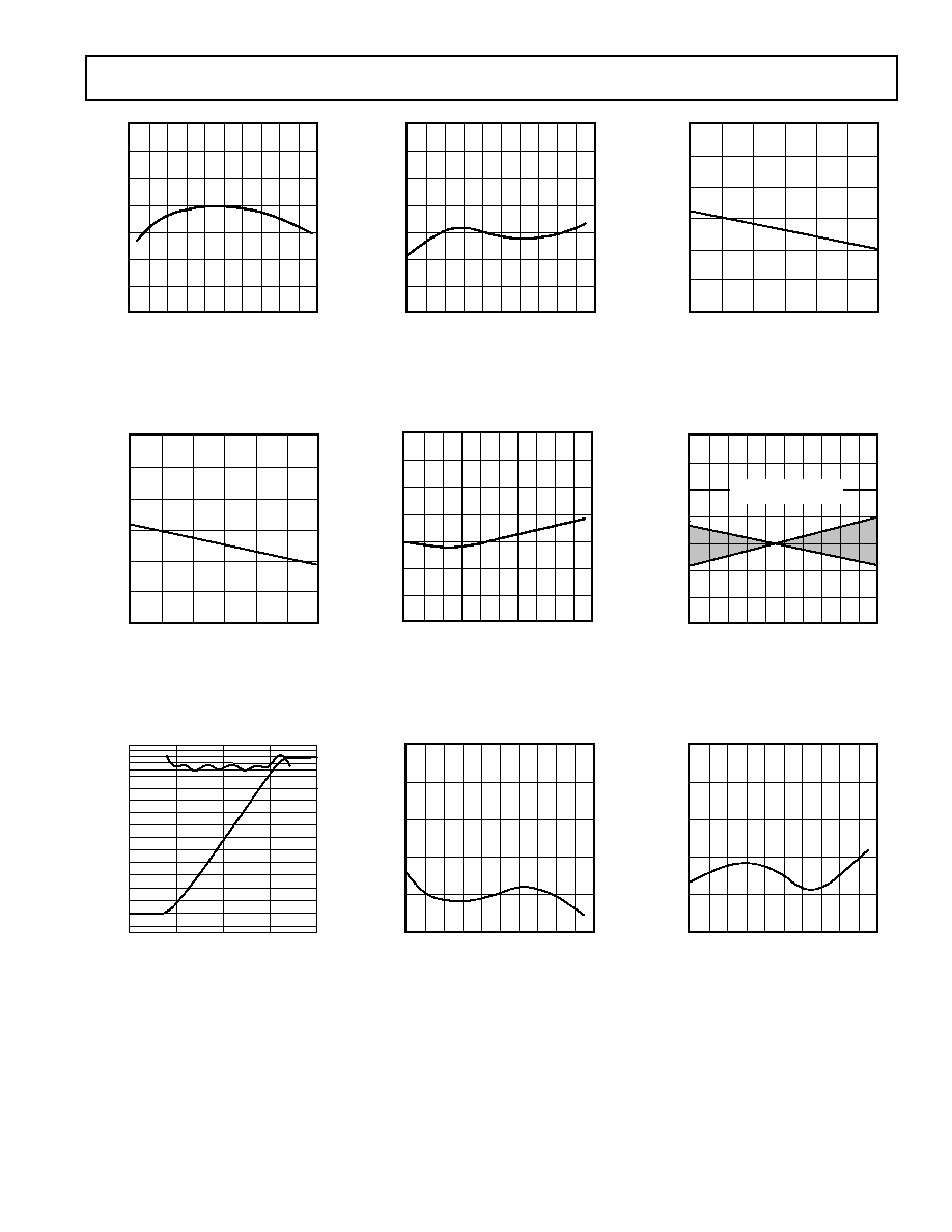
Typical DC Performance Characteristics≠AD640
REV. C
≠5≠
1.015
1.010
1.005
1
0.995
0.990
0.985
0.980
≠60 ≠40 ≠20
0
20
40 60 80 100 120 140
TEMPERATURE ≠ C
SLOPE CURRENT ≠ mA
Figure 1. Slope Current, I
Y
vs.
Temperature
4.5
5.0
5.5
6.0
6.5
7.0
7.5
POWER SUPPLY VOLTAGES ≠ Volts
INTERCEPT VOLTAGE ≠ mV
1.015
1.010
1.005
1.000
0.995
0.990
0.985
Figure 4. Intercept Voltage, V
X
, vs.
Supply Voltages
INPUT VOLTAGE ≠ mV
(EITHER SIGN)
OUTPUT CURRENT ≠ mA
2
1.0
0.1
1.0
1000.0
10.0
100.0
1
1.2
1.4
1.6
1.8
2.0
2.2
2.4
0.8
0.6
0.4
0.2
0
≠0.2
≠0.4
ERROR ≠ dB
0
Figure 7. DC Logarithmic Transfer
Function and Error Curve for Single
AD640
1.20
1.15
1.10
1.05
1.00
0.95
0.90
≠60 ≠40 ≠20
0
20
40
60 80 100 120 140
TEMPERATURE ≠ C
INTERCEPT ≠ mV
0.85
Figure 2. Intercept Voltage, V
X
, vs.
Temperature
14
13
12
11
10
9
8
7
≠60 ≠40 ≠20
0
20 40
60 80 100 120 140
TEMPERATURE ≠ C
INTERCEPT ≠ mV
Figure 5. Intercept Voltage (Using
Attenuator) vs. Temperature
2.5
2.0
1.5
1.0
0.5
≠60 ≠40 ≠20
0
20 40 60
80 100 120 140
TEMPERATURE ≠ C
0
ABSOLUTE ERROR ≠ dB
Figure 8. Absolute Error vs. Tem-
perature, V
IN
= 1 mV to 100 mV
4.5
5.0
5.5
6.0
6.5
7.0
7.5
POWER SUPPLY VOLTAGES ≠ Volts
SLOPE CURRENT ≠ mA
1.006
1.004
1.002
1.000
0.998
0.996
0.994
Figure 3. Slope Current, I
Y
vs.
Supply Voltages
≠60 ≠40 ≠20
0
20
40 60 80 100 120 140
TEMPERATURE ≠ C
DEVIATION OF INPUT OFFSET VOLTAGE ≠ mV
0
≠0.1
+0.4
+0.3
+0.2
+0.1
≠0.2
≠0.3
INPUT OFFSET VOLTAGE
DEVIATION WILL BE WITHIN
SHADED AREA.
Figure 6. Input Offset Voltage
Deviation vs. Temperature
2.5
2.0
1.5
1.0
0.5
≠60 ≠40 ≠20
0
20
40 60
80 100 120 140
TEMPERATURE ≠ C
0
ABSOLUTE ERROR ≠ dB
Figure 9. Absolute Error vs.
Temperature, Using Attenuator.
V
IN
= 10 mV to 1 V, Pin 8
Grounded to Disable ITC Bias