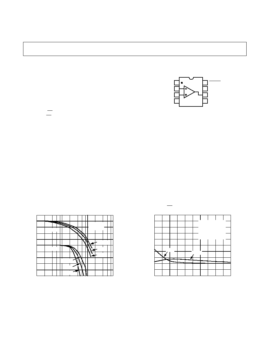
CONNECTION DIAGRAM
8-Pin Plastic Mini-DIP (N), SOIC (R)
and Cerdip (Q) Packages
OFFSET
NULL
1
2
3
4
8
7
6
5
TOP VIEW
AD810
DISABLE
+V
S
OUTPUT
OFFSET
NULL
≠IN
+IN
≠V
S
REV. A
Information furnished by Analog Devices is believed to be accurate and
reliable. However, no responsibility is assumed by Analog Devices for its
use, nor for any infringements of patents or other rights of third parties
which may result from its use. No license is granted by implication or
otherwise under any patent or patent rights of Analog Devices.
a
Low Power
Video Op Amp with Disable
AD810
One Technology Way, P.O. Box 9106, Norwood, MA 02062-9106, U.S.A.
Tel: 617/329-4700
Fax: 617/326-8703
FEATURES
High Speed
80 MHz Bandwidth (3 dB, G = +1)
75 MHz Bandwidth (3 dB, G = +2)
1000 V/ s Slew Rate
50 ns Settling Time to 0.1% (V
O
= 10 V Step)
Ideal for Video Applications
30 MHz Bandwidth (0.1 dB, G = +2)
0.02% Differential Gain
0.04 Differential Phase
Low Noise
2.9 nV/
Hz Input Voltage Noise
13 pA/
Hz Inverting Input Current Noise
Low Power
8.0 mA Supply Current max
2.1 mA Supply Current (Power-Down Mode)
High Performance Disable Function
Turn-Off Time 100 ns
Break Before Make Guaranteed
Input to Output Isolation of 64 dB (OFF State)
Flexible Operation
Specified for 5 V and 15 V Operation
2.9 V Output Swing Into a 150 Load (V
S
= 5 V)
APPLICATIONS
Professional Video Cameras
Multimedia Systems
NTSC, PAL & SECAM Compatible Systems
Video Line Driver
ADC/DAC Buffer
DC Restoration Circuits
PRODUCT DESCRIPTION
The AD810 is a composite and HDTV compatible, current
feedback, video operational amplifier, ideal for use in systems
such as multimedia, digital tape recorders and video cameras.
The 0.1 dB flatness specification at bandwidth of 30 MHz
(G = +2) and the differential gain and phase of 0.02% and
0.04
∞
(NTSC) make the AD810 ideal for any broadcast quality
video system. All these specifications are under load conditions
of 150
(one 75
back terminated cable).
The AD810 is ideal for power sensitive applications such as
video cameras, offering a low power supply current of 8.0 mA
max. The disable feature reduces the power supply current to
only 2.1 mA, while the amplifier is not in use, to conserve
power. Furthermore the AD810 is specified over a power supply
range of
±
5 V to
±
15 V.
The AD810 works well as an ADC or DAC buffer in video
systems due to its unity gain bandwidth of 80 MHz. Because the
AD810 is a transimpedance amplifier, this bandwidth can be
maintained over a wide range of gains while featuring a low
noise of 2.9 nV/
Hz
for wide dynamic range applications.
0.10
0
15
0.03
0.01
6
0.02
5
0.06
0.04
0.05
0.07
0.08
0.09
14
13
12
11
10
9
8
7
0.20
0.18
0.16
0.14
0.12
0.10
0.08
0.06
0.04
0.02
0
GAIN
PHASE
GAIN = +2
R
F
= 715
R
L
= 150
f
C
= 3.58MHz
100 IRE
MODULATED RAMP
SUPPLY VOLTAGE ≠ ± Volts
DIFFERENTIAL GAIN ≠ %
DIFFERENTIAL PHASE ≠ Degrees
Differential Gain and Phase vs. Supply Voltage
GAIN = +2
R
L
= 150
±2.5V
±5V
±2.5V
PHASE
GAIN
0
≠5
10
100
≠1
≠2
≠3
≠4
1
1
1000
0
≠45
≠90
≠135
≠180
≠225
≠270
CLOSED-LOOP GAIN ≠ dB
PHASE SHIFT ≠ Degrees
FREQUENCY ≠ MHz
±5V
V
S
= ±15V
V
S
= ±15V
Closed-Loop Gain and Phase vs. Frequency, G = +2,
R
L
= 150, R
F
= 715

REV. A
≠2≠
AD810≠SPECIFICATIONS
(@ T
A
= +25 C and V
S
= 15 V dc, R
L
= 150
unless otherwise noted)
AD810A
AD810S
1
Parameter
Conditions
V
S
Min
Typ
Max
Min
Typ
Max
Units
DYNAMIC PERFORMANCE
3 dB Bandwidth
(G = +2) R
FB
= 715
±
5 V
40
50
40
50
MHz
(G = +2) R
FB
= 715
±
15 V
55
75
55
75
MHz
(G = +1) R
FB
= 1000
±
15 V
40
80
40
80
MHz
(G = +10) R
FB
= 270
±
15 V
50
65
50
65
MHz
0.1 dB Bandwidth
(G = +2) R
FB
= 715
±
5 V
13
22
13
22
MHz
(G = +2) R
FB
= 715
±
15 V
15
30
15
30
MHz
Full Power Bandwidth
V
O
= 20 V p-p,
R
L
= 400
±
15 V
16
16
MHz
Slew Rate
2
R
L
= 150
±
5 V
350
350
V/
µ
s
R
L
= 400
±
15 V
1000
1000
V/
µ
s
Settling Time to 0.1%
10 V Step, G = ≠1
±
15 V
50
50
ns
Settling Time to 0.01%
10 V Step, G = ≠1
±
15 V
125
125
ns
Differential Gain
f = 3.58 MHz
±
15 V
0.02
0.05
0.02
0.05
%
f - 3.58 MHz
±
5 V
0.04
0.07
0.04
0.07
%
Differential Phase
f = 3.58 MHz
±
15 V
0.04
0.07
0.04
0.07
Degrees
f = 3.58 MHz
±
5 V
0.045
0.08
0.045
0.08
Degrees
Total Harmonic Distortion
f = 10 MHz, V
O
= 2 V p-p
R
L
= 400
, G = +2
±
15 V
≠61
≠61
dBc
INPUT OFFSET VOLTAGE
±
5 V,
±
15 V
1.5
6
1.5
6
mV
T
MIN
≠T
MAX
±
5 V,
±
15 V
2
7.5
4
15
mV
Offset Voltage Drift
7
15
µ
V/
∞
C
INPUT BIAS CURRENT
≠Input
T
MIN
≠T
MAX
±
5 V,
±
15 V
0.7
5
0.8
5
µ
A
+Input
T
MIN
≠T
MAX
±
5 V,
±
15 V
2
7.5
2
10
µ
A
OPEN-LOOP
T
MIN
≠T
MAX
TRANSRESISTANCE
V
O
=
±
10 V, R
L
= 400
±
15 V
1.0
3.5
1.0
3.5
M
V
O
=
±
2.5 V, R
L
= 100
±
5 V
0.3
1.2
0.2
1.0
M
OPEN-LOOP
T
MIN
≠T
MAX
DC VOLTAGE GAIN
V
O
=
±
10 V, R
L
= 400
±
15 V
86
100
80
100
dB
V
O
=
±
2.5 V, R
L
= 100
±
5 V
76
88
72
88
dB
COMMON-MODE REJECTION
T
MIN
≠T
MAX
V
OS
V
CM
=
±
12 V
±
15 V
56
64
56
64
dB
V
CM
=
±
2.5 V
±
5 V
52
60
50
60
dB
±
Input Current
T
MIN
≠T
MAX
±
5 V,
±
15 V
0.1
0.4
0.1
0.4
µ
A/V
POWER SUPPLY REJECTION
±
4.5 V to
±
18 V
V
OS
T
MIN
≠T
MAX
65
72
60
72
dB
±
Input Current
T
MIN
≠T
MAX
0.05
0.3
0.05
0.3
µ
A/V
INPUT VOLTAGE NOISE
f = 1 kHz
±
5 V,
±
15 V
2.9
2.9
nV/
Hz
INPUT CURRENT NOISE
≠I
IN
, f = 1 kHz
±
5 V,
±
15 V
13
13
pA/
Hz
+I
IN
, f = 1 kHz
±
5 V,
±
15 V
1.5
1.5
pA/
Hz
INPUT COMMON-MODE
±
5 V
±
2.5
±
3.0
±
2.5
±
3
V
VOLTAGE RANGE
±
15 V
±
12
±
13
±
12
±
13
V
OUTPUT CHARACTERISTICS
Output Voltage Swing
3
R
L
= 150
, T
MIN
≠T
MAX
±
5 V
±
2.5
±
2.9
±
2.5
±
2.9
V
R
L
= 400
±
15 V
±
12.5
±
12.9
±
12.5
±
12.9
V
R
L
= 400
, T
MIN
≠T
MAX
±
15 V
±
12
±
12
V
Short-Circuit Current
±
15 V
150
150
mA
Output Current
T
MIN
≠T
MAX
±
5 V,
±
15 V
40
60
30
60
mA
OUTPUT RESISTANCE
Open Loop (5 MHz)
15
15
INPUT CHARACTERISTICS
Input Resistance
+Input
±
15 V
2.5
10
2.5
10
M
≠Input
±
15 V
40
40
Input Capacitance
+Input
±
15 V
2
2
pF
DISABLE CHARACTERISTICS
4
OFF Isolation
f = 5 MHz, See Figure 43
64
64
dB
OFF Output Impedance
See Figure 43
(R
F
+ R
G
) 13 pF
(R
F
+ R
G
) 13 pF
ABSOLUTE MAXIMUM RATINGS
1
Supply Voltage . . . . . . . . . . . . . . . . . . . . . . . . . . . . . . . .
±
18 V
Internal Power Dissipation
2
. . . . . . . Observe Derating Curves
Output Short Circuit Duration . . . . Observe Derating Curves
Common-Mode Input Voltage . . . . . . . . . . . . . . . . . . . . . .
±
V
S
Differential Input Voltage . . . . . . . . . . . . . . . . . . . . . . . .
±
6 V
Storage Temperature Range
Plastic DIP . . . . . . . . . . . . . . . . . . . . . . . . ≠65
∞
C to +125
∞
C
Cerdip . . . . . . . . . . . . . . . . . . . . . . . . . . . ≠65
∞
C to +150
∞
C
Small Outline IC . . . . . . . . . . . . . . . . . . . ≠65
∞
C to +125
∞
C
Operating Temperature Range
AD810A . . . . . . . . . . . . . . . . . . . . . . . . . . . ≠40
∞
C to +85
∞
C
AD810S . . . . . . . . . . . . . . . . . . . . . . . . . . ≠55
∞
C to +125
∞
C
Lead Temperature Range (Soldering 60 sec) . . . . . . . +300
∞
C
NOTES
1
Stresses above those listed under "Absolute Maximum Ratings" may cause
permanent damage to the device. This is a stress rating only and functional
operation of the device at these or any other conditions above those indicated in the
operational section of this specification is not implied. Exposure to absolute
maximum raring conditions for extended periods may affect device reliability.
2
8-Pin Plastic Package:
JA
= 90
∞
C/Watt; 8-Pin Cerdip Package:
JA
= 110
∞
C/Watt;
8-Pin SOIC Package:
JA
= 150
∞
C/Watt.
ESD SUSCEPTIBILITY
ESD (electrostatic discharge) sensitive device. Electrostatic
charges as high as 4000 volts, which readily accumulate on the
human body and on test equipment, can discharge without
detection. Although the AD810 features ESD protection
circuitry, permanent damage may still occur on these devices if
they are subjected to high energy electrostatic discharges.
Therefore, proper ESD precautions are recommended to avoid
any performance degradation or loss of functionality.
ORDERING GUIDE
Temperature
Package
Package
Model
Range
Description
Option
AD810AN
≠40
∞
C to +85
∞
C
8-Pin Plastic DIP
N-8
AD810AR
≠40
∞
C to +85
∞
C
8-Pin Plastic SOIC R-8
AD810AR-REEL
≠40
∞
C to +85
∞
C
8-Pin Plastic SOIC R-8
5962-9313201MPA ≠55
∞
C to +125
∞
C 8-Pin Cerdip
Q-8
AD810A
AD810S
1
Parameter
Conditions
V
S
Min
Typ
Max
Min
Typ
Max
Units
Turn On Time
5
Z
OUT
= Low, See Figure 54
170
170
ns
Turn Off Time
Z
OUT
= High
100
100
ns
Disable Pin Current
Disable Pin = 0 V
±
5 V
50
75
50
75
µ
A
±
15 V
290
400
290
400
µ
A
Min Disable Pin Current to
Disable
T
MIN
≠T
MAX
±
5 V,
±
15 V
30
30
µ
A
POWER SUPPLY
Operating Range
+25
∞
C to T
MAX
±
2.5
±
18
±
2.5
±
18
V
T
MIN
±
3.0
±
18
±
3.5
±
18
V
Quiescent Current
±
5 V
6.7
7.5
6.7
7.5
mA
±
15 V
6.8
8.0
6.8
8.0
mA
T
MIN
≠T
MAX
±
5 V,
±
15 V
8.3
10.0
9
11.0
mA
Power-Down Current
±
5 V
1.8
2.3
1.8
2.3
mA
±
15 V
2.1
2.8
2.1
2.8
mA
NOTES
1
See Analog Devices Military Data Sheet for 883B Specifications.
2
Slew rate measurement is based on 10% to 90% rise time with the amplifier configured for a gain of ≠10.
3
Voltage Swing is defined as useful operating range, not the saturation range.
4
Disable guaranteed break before make.
5
Turn On Time is defined with
±
5 V supplies using complementary output CMOS to drive the disable pin.
Specifications subject to change without notice.
MAXIMUM POWER DISSIPATION
The maximum power that can be safely dissipated by the
AD810 is limited by the associated rise in junction temperature.
For the plastic packages, the maximum safe junction tempera-
ture is 145
∞
C. For the cerdip package, the maximum junction
temperature is 175
∞
C. If these maximums are exceeded momen-
tarily, proper circuit operation will be restored as soon as the die
temperature is reduced. Leaving the device in the "overheated"
condition for an extended period can result in device burnout.
To ensure proper operation, it is important to observe the
derating curves.
2.4
0.4
140
1.0
0.6
≠40
0.8
≠60
1.6
1.2
1.4
1.8
2.0
2.2
120
100
80
60
40
20
0
≠20
TOTAL POWER
DISSIPATION ≠ Watts
8-PIN
MINI-DIP
AMBIENT TEMPERATURE ≠
∞
C
8-PIN
SOIC
8-PIN
CERDIP
8-PIN
MINI-DIP
Maximum Power Dissipation vs. Temperature
While the AD810 is internally short circuit protected, this may
not be sufficient to guarantee that the maximum junction
temperature is not exceeded under all conditions.
1
5
2
3
0.1µF
+V
S
6
AD810
0.1µF
≠V
S
10k
SEE TEXT
7
4
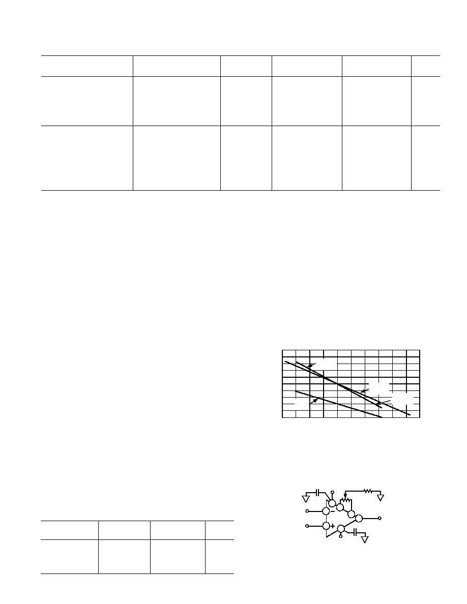
Offset Null Configuration
AD810
REV. A
≠3≠
AD810
REV. A
≠4≠
20
5
0
20
15
10
5
15
10
0
MAGNITUDE OF THE OUTPUT VOLTAGE ≠ ±Volts
SUPPLY VOLTAGE ≠ ±Volts
NO LOAD
R
L
= 150
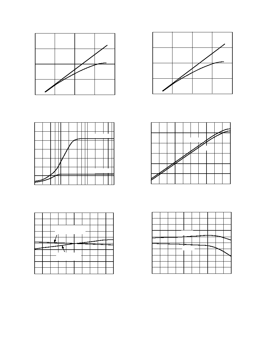
Figure 1. Input Common-Mode Voltage Range vs.
Supply Voltage
35
10
0
10
100
10k
1k
25
5
15
20
30
OUTPUT VOLTAGE ≠ Volts p-p
LOAD RESISTANCE ≠ Ohms
±15V SUPPLY
±5V SUPPLY
Figure 3. Output Voltage Swing vs. Load Resistance
≠10
140
≠40
≠60
120
100
80
60
40
20
0
≠20
INPUT BIAS CURRENT ≠ µA
JUNCTION TEMPERATURE ≠
∞
C
10
8
6
4
2
0
≠2
≠4
≠6
≠8
INVERTING INPUT
V
S
= ±5V, ±15V
NONINVERTING INPUT
V
S
= ±5V, ±15V
Figure 5. Input Bias Current vs. Temperature
≠Typical Characteristics
20
5
0
20
15
10
5
15
10
0
MAGNITUDE OF THE OUTPUT VOLTAGE ≠ ±Volts
SUPPLY VOLTAGE ≠ ±Volts
NO LOAD
R
L
= 150
Figure 2. Output Voltage Swing vs. Supply
10
4
140
7
5
≠40
6
≠60
9
8
120
80
60
40
100
20
0
≠20
SUPPLY CURRENT ≠ mA
JUNCTION TEMPERATURE ≠
∞
C
V
S
= ±15V
V
S
= ±5V
Figure 4. Supply Current vs. Junction Temperature
10
≠8
140
≠4
≠6
≠40
≠60
2
≠2
4
6
8
120
100
80
60
40
20
0
≠20
INPUT OFFSET VOLTAGE ≠ mV
JUNCTION TEMPERATURE ≠
∞
C
0
≠10
V
S
= ±15V
V
S
= ±5V
Figure 6. Input Offset Voltage vs. Junction Temperature
AD810
REV. A
≠5≠
250
50
≠60
+140
200
100
≠40
150
+100 +120
+80
+60
+40
+20
0
≠20
SHORT CIRCUIT CURRENT ≠ mA
JUNCTION TEMPERATURE ≠
∞
C
V
S
= ±15V
V
S
= ±5V
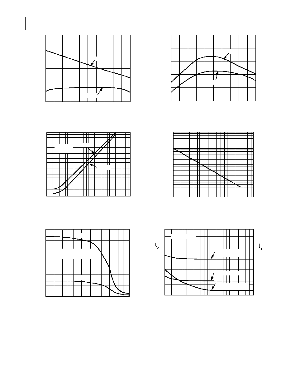
Figure 7. Short Circuit Current vs. Temperature
10.0
0.01
100k
100M
10M
1M
10k
1.0
0.1
CLOSED-LOOP OUTPUT RESISTANCE ≠
FREQUENCY ≠ Hz
V
S
= ±5V
GAIN = 2
R
F
= 715
V
S
= ±15V
Figure 9. Closed-Loop Output Resistance vs. Frequency
30
15
0
100k
1M
100M
10M
10
5
20
25
FREQUENCY ≠ Hz
OUTPUT VOLTAGE ≠ Volts p-p
OUTPUT LEVEL FOR 3% THD
R
L
= 400
V
S
= ±15V
±
V
S
= ±5V
Figure 11. Large Signal Frequency Response
Typical Characteristics≠
120
20
+140
80
40
≠40
60
≠60
100
+120
+100
+80
+60
+40
+20
0
≠20
OUTPUT CURRENT ≠ mA
JUNCTION TEMPERATURE ≠
∞
C
V
S
= 15V
V
S
= 5V
±
±
Figure 8. Linear Output Current vs. Temperature
100k
10k
1k
100
100k
1M
10M
100M
OUTPUT RESISTANCE ≠
FREQUENCY ≠ Hz
1M
Figure 10. Output Resistance vs. Frequency,
Disabled State
100
10
1
100
10
1
10
100
1k
10k
100k
INVERTING INPUT
CURRENT NOISE
VOLTAGE NOISE
FREQUENCY ≠ Hz
V
S
= ±5V TO ±15V
NONINVERTING INPUT
CURRENT NOISE
CURRENT NOISE ≠ pA/ Hz
VOLTAGE NOISE ≠ nV/ Hz
Figure 12. Input Voltage and Current Noise vs. Frequency