Document Outline
- FEATURES
- APPLICATIONS
- PRODUCT DESCRIPTION
- CONNECTION DIAGRAM
- SPECIFICATIONS
- ABSOLUTE MAXIMUM RATINGS
- MAXIMUM POWER DISSIPATION
- ORDERING GUIDE
- Typical Performance Characteristics
- Overdrive Recovery
- Circuit Description
- Output Impedance
- Disable Operation
- Single-Supply A/D Conversion
- APPLICATIONS
- RGB Buffer
- Single-Supply Composite Video Line Driver
- Sync Stripper
- Layout Considerations
- OUTLINE DIMENSIONS
- Revision History

REV. B
Information furnished by Analog Devices is believed to be accurate and
reliable. However, no responsibility is assumed by Analog Devices for its
use, nor for any infringements of patents or other rights of third parties that
may result from its use. No license is granted by implication or otherwise
under any patent or patent rights of Analog Devices. Trademarks and
registered trademarks are the property of their respective companies.
One Technology Way, P.O. Box 9106, Norwood, MA 02062-9106, U.S.A.
Tel: 781/329-4700
www.analog.com
Fax: 781/326-8703
© 2003 Analog Devices, Inc. All rights reserved.
AD8041
*
160 MHz Rail-to-Rail
Amplifier with Disable
*Protected by U.S.Patent No. 5,537,079.
FEATURES
Fully Specified for +3 V, +5 V, and 5 V Supplies
Output Swings Rail to Rail
Input Voltage Range Extends 200 mV Below Ground
No Phase Reversal with Inputs 1 V Beyond Supplies
Disable/Power-Down Capability
Low Power of 5.2 mA (26 mW on 5 V)
High Speed and Fast Settling on 5 V:
160 MHz ≠3 dB Bandwidth (G = +1)
160 V/ s Slew Rate
30 ns Settling Time to 0.1%
Good Video Specifications (R
L
= 150 , G = +2)
Gain Flatness of 0.1 dB to 30 MHz
0.03% Differential Gain Error
0.03 Differential Phase Error
Low Distortion
≠69 dBc Worst Harmonic @ 10 MHz
Outstanding Load Drive Capability
Drives 50 mA 0.5 V from Supply Rails
Cap Load Drive of 45 pF
APPLICATIONS
Power Sensitive High Speed Systems
Video Switchers
Distribution Amplifiers
A/D Drivers
Professional Cameras
CCD Imaging Systems
Ultrasound Equipment (Multichannel)
Single-Supply Multiplexer
CONNECTION DIAGRAM
8-Lead PDIP, CERDIP and SOIC
V
S
DISABLE
1
2
3
4
8
7
6
5
NC = NO CONNECT
NC
NC
OUTPUT
≠INPUT
INPUT
≠V
S
AD8041
(Top View)
PRODUCT DESCRIPTION
The AD8041 is a low power voltage feedback, high speed ampli-
fier designed to operate on +3 V, +5 V, or
±5 V supplies. It has
true single-supply capability with an input voltage range extending
200 mV below the negative rail and within 1 V of the positive rail.
5V
2.5V
0V
200ns
1V
Figure 1. Output Swing: G = ≠1, V
S
= 5 V
The output voltage swing extends to within 50 mV of each rail,
providing the maximum output dynamic range. Additionally, it
features gain flatness of 0.1 dB to 30 MHz while offering differ-
ential gain and phase error of 0.03% and 0.03
∞ on a single 5 V
supply. This makes the AD8041 ideal for professional video
electronics such as cameras, video switchers, or any high speed
portable equipment. The AD8041's low distortion and fast settling
make it ideal for buffering high speed A-to-D converters.
The AD8041 has a high speed disable feature useful for mul-
tiplexing or for reducing power consumption (1.5 mA). The
disable logic interface is compatible with CMOS or open-
collector logic. The AD8041 offers a low power supply current
of 5.8 mA maximum and can run on a single 3 V power supply.
These features are ideally suited for portable and battery-
powered applications where size and power are critical.
The wide bandwidth of 160 MHz along with 160 V/
µs of slew
rate on a single 5 V supply make the AD8041 useful in many
general-purpose high speed applications where dual power
supplies of up to
±6 V and single supplies from 3 V to 12 V are
needed. The AD8041 is available in 8-lead PDIP and SOIC
over the industrial temperature range of ≠40
∞C to +85∞C.
FREQUENCY (MHz)
V
S
= 5V
G = +2
R
F
= 400
0
100
NORMALIZED GAIN (dB)
80
60
40
20
0
2
1
≠2
≠1
≠8
≠7
≠6
≠5
≠4
≠3
Figure 2. Frequency Response: G = +2, V
S
= 5 V

REV. B
≠2≠
AD8041≠SPECIFICATIONS
(@ T
A
= 25 C, V
S
= 5 V, R
L
= 2 k to 2.5 V, unless otherwise noted.)
AD8041A
Parameter
Conditions
Min
Typ
Max
Unit
DYNAMIC PERFORMANCE
≠3 dB Small Signal Bandwidth, V
O
< 0.5 V p-p
G = +1
130
160
MHz
Bandwidth for 0.1 dB Flatness
G = +2, R
L
= 150
30
MHz
Slew Rate
G = ≠1, V
O
= 2 V Step
130
160
V/
µs
Full Power Response
V
O
= 2 V p-p
24
MHz
Settling Time to 0.1%
G = ≠1, V
O
= 2 V Step
35
ns
Settling Time to 0.01%
55
ns
NOISE/DISTORTION PERFORMANCE
Total Harmonic Distortion
f
C
= 5 MHz, V
O
= 2 V p-p, G = +2, R
L
= 1 k
≠72
dB
Input Voltage Noise
f = 10 kHz
16
nV/
Hz
Input Current Noise
f = 10 kHz
600
fA/
Hz
Differential Gain Error (NTSC)
G = +2, R
L
= 150
to 2.5 V
0.03
%
G = +2, R
L
= 75
to 2.5 V
0.01
%
Differential Phase Error (NTSC)
G = +2, R
L
= 150
to 2.5 V
0.03
Degrees
G = +2, R
L
= 75
to 2.5 V
0.19
Degrees
DC PERFORMANCE
Input Offset Voltage
2
7
mV
T
MIN
to T
MAX
8
mV
Offset Drift
10
µV/∞C
Input Bias Current
1.2
3.2
µA
T
MIN
to T
MAX
3.5
µA
Input Offset Current
0.2
0.5
µA
Open-Loop Gain
R
L
= 1 k
86
95
dB
T
MIN
to T
MAX
90
dB
INPUT CHARACTERISTICS
Input Resistance
160
k
Input Capacitance
1.8
pF
Input Common-Mode Voltage Range
≠0.2 to +4
V
Common-Mode Rejection Ratio
V
CM
= 0 V to 3.5 V
74
80
dB
OUTPUT CHARACTERISTICS
Output Voltage Swing: R
L
= 10 k
0.05 to 4.95
V
Output Voltage Swing:
R
L
= 1 k
0.35 to 4.75
0.1 to 4.9
V
Output Voltage Swing:
R
L
= 50
0.4 to 4.4
0.3 to 4.5
V
Output Current
V
OUT
= 0.5 V to 4.5 V
50
mA
Short-Circuit Current
Sourcing
90
mA
Sinking
150
mA
Capacitive Load Drive
G = +1
45
pF
POWER SUPPLY
Operating Range
3
12
V
Quiescent Current
5.2
5.8
mA
Quiescent Current (Disabled)
1.4
1.7
mA
Power Supply Rejection Ratio
V
S
= 0, +5 V,
±1 V
72
80
dB
DISABLE CHARACTERISTICS
V
O
= 2 V p-p @ 10 MHz, G = +2
Turn-Off Time
R
F
= R
L
= 2 k
120
ns
Turn-On Time
R
F
= R
L
= 2 k
230
ns
Off Isolation (Pin 8 Tied to ≠V
S
)
R
L
= 100
, f = 5 MHz, G = +2, R
F
= 1 k
70
dB
Off Voltage (Device Disabled)
<V
S
≠ 2.5
V
On Voltage (Device Enabled)
Open or +V
S
V
Specifications subject to change without notice.

REV. B
AD8041
≠3≠
SPECIFICATIONS
(@ T
A
= 25 C, V
S
= 3 V, R
L
= 2 k to 1.5 V, unless otherwise noted.)
AD8041A
Parameter
Conditions
Min
Typ
Max
Unit
DYNAMIC PERFORMANCE
≠3 dB Small Signal Bandwidth, V
O
< 0.5 V p-p
G = +1
120
150
MHz
Bandwidth for 0.1 dB Flatness
G = +2, R
L
= 150
25
MHz
Slew Rate
G = ≠1, V
O
= 2 V Step
120
150
V/
µs
Full Power Response
V
O
= 2 V p-p
20
MHz
Settling Time to 0.1%
G = ≠1, V
O
= 2 V Step
40
ns
Settling Time to 0.01%
55
ns
NOISE/DISTORTION PERFORMANCE
Total Harmonic Distortion
f
C
= 5 MHz, V
O
= 2 V p-p, G = ≠1, R
L
= 100
≠55
dB
Input Voltage Noise
f = 10 kHz
16
nV/
Hz
Input Current Noise
f = 10 kHz
600
fA/
Hz
Differential Gain Error (NTSC)
G = +2, R
L
= 150
to 1.5 V, Input V
CM
= 1 V
0.07
%
Differential Phase Error (NTSC)
G = +2, R
L
= 150
to 1.5 V, Input V
CM
= 1 V
0.05
Degrees
DC PERFORMANCE
Input Offset Voltage
2
7
mV
T
MIN
to T
MAX
8
mV
Offset Drift
10
µV/∞C
Input Bias Current
1.2
3.2
µA
T
MIN
to T
MAX
3.5
µA
Input Offset Current
0.2
0.6
µA
Open-Loop Gain
R
L
= 1 k
85
94
dB
T
MIN
to T
MAX
89
dB
INPUT CHARACTERISTICS
Input Resistance
160
k
Input Capacitance
1.8
pF
Input Common-Mode Voltage Range
≠0.2 to +2
V
Common-Mode Rejection Ratio
V
CM
= 0 V to 1.5 V
72
80
dB
OUTPUT CHARACTERISTICS
Output Voltage Swing: R
L
= 10 k
0.05 to 2.95
V
Output Voltage Swing:
R
L
= 1 k
0.45 to 2.7
0.1 to 2.9
V
Output Voltage Swing:
R
L
= 50
0.5 to 2.6
0.25 to 2.75
V
Output Current
V
OUT
= 0.5 V to 2.5 V
50
mA
Short-Circuit Current
Sourcing
70
mA
Sinking
120
mA
Capacitive Load Drive
G = +1
40
pF
POWER SUPPLY
Operating Range
3
12
V
Quiescent Current
5.0
5.6
mA
Quiescent Current (Disabled)
1.3
1.5
mA
Power Supply Rejection Ratio
V
S
= 0, +3 V,
±0.5 V
68
80
dB
DISABLE CHARACTERISTICS
V
O
= 2 V p-p @ 10 MHz, G = +2
Turn-Off Time
R
F
= R
L
= 2 k
90
ns
Turn-On Time
R
F
= R
L
= 2 k
170
ns
Off Isolation (Pin 8 Tied to ≠V
S
)
R
L
= 100
, f = 5 MHz, G = +2, R
F
= 1 k
70
dB
Off Voltage (Device Disabled)
<V
S
≠ 2.5
V
On Voltage (Device Enabled)
Open or +V
S
V
Specifications subject to change without notice.

REV. B
≠4≠
AD8041
SPECIFICATIONS
(@ T
A
= 25 C, V
S
= 5 V, R
L
= 2 k to 0 V, unless otherwise noted.)
AD8041A
Parameter
Conditions
Min
Typ
Max
Unit
DYNAMIC PERFORMANCE
≠3 dB Small Signal Bandwidth, V
O
< 0.5 V p-p
G = +1
140
170
MHz
Bandwidth for 0.1 dB Flatness
G = +2, R
L
= 150
32
MHz
Slew Rate
G = ≠1, V
O
= 2 V Step
140
170
V/
µs
Full Power Response
V
O
= 2 V p-p
26
MHz
Settling Time to 0.1%
G = ≠1, V
O
= 2 V Step
30
ns
Settling Time to 0.01%
50
ns
NOISE/DISTORTION PERFORMANCE
Total Harmonic Distortion
f
C
= 5 MHz, V
O
= 2 V p-p, G = +2, R
L
= 1 k
≠77
dB
Input Voltage Noise
f = 10 kHz
16
nV/
Hz
Input Current Noise
f = 10 kHz
600
fA/
Hz
Differential Gain Error (NTSC)
G = +2, R
L
= 150
0.02
%
G = +2, R
L
= 75
0.02
%
Differential Phase Error (NTSC)
G = +2, R
L
= 150
0.03
Degrees
G = +2, R
L
= 75
0.10
Degrees
DC PERFORMANCE
Input Offset Voltage
2
7
mV
T
MIN
to T
MAX
8
mV
Offset Drift
10
µV/∞C
Input Bias Current
1.2
3.2
µA
T
MIN
to T
MAX
3.5
µA
Input Offset Current
0.2
0.6
µA
Open-Loop Gain
R
L
= 1 k
90
99
dB
T
MIN
to T
MAX
95
dB
INPUT CHARACTERISTICS
Input Resistance
160
k
Input Capacitance
1.8
pF
Input Common-Mode Voltage Range
≠5.2 to +4
V
Common-Mode Rejection Ratio
V
CM
= ≠5 V to +3.5 V
72
80
dB
OUTPUT CHARACTERISTICS
Output Voltage Swing: R
L
= 10 k
≠4.95 to +4.95
V
Output Voltage Swing:
R
L
= 1 k
≠4.45 to +4.6
≠4.8 to +4.8
V
Output Voltage Swing:
R
L
= 50
≠4.3 to +3.2
≠4.5 to +3.8
V
Output Current
V
OUT
= ≠4.5 V to +4.5 V
50
mA
Short-Circuit Current
Sourcing
100
mA
Sinking
160
mA
Capacitive Load Drive
G = +1
50
pF
POWER SUPPLY
Operating Range
3
12
V
Quiescent Current
5.8
6.5
mA
Quiescent Current (Disabled)
1.6
2.2
mA
Power Supply Rejection Ratio
V
S
= ≠5 V, +5 V,
±1 V
68
80
dB
DISABLE CHARACTERISTICS
V
O
= 2 V p-p @ 10 MHz, G = +2
Turn-Off Time
R
F
= 2 k
120
ns
Turn-On Time
R
F
= 2 k
320
ns
Off Isolation (Pin 8 Tied to ≠V
S
)
R
L
= 100
, f = 5 MHz, G = +2, R
F
= 1 k
70
dB
Off Voltage (Device Disabled)
<V
S
≠ 2.5
V
On Voltage (Device Enabled)
Open or +V
S
V
Specifications subject to change without notice.
REV. B
AD8041
≠5≠
ABSOLUTE MAXIMUM RATINGS
1
Supply Voltage ............................................................ 12.6 V
Internal Power Dissipation
2
PDIP Package (N) .................................................... 1.3 W
SOIC Package (R) .................................................... 0.9 W
Input Voltage (Common Mode) ......................................
± V
S
Differential Input Voltage ...........................................
± 3.4 V
Output Short-Circuit Duration
.......................................... Observe Power Derating Curves
Storage Temperature Range N, R .............. ≠65
∞C to +125∞C
Operating Temperature Range (A Grade) ... ≠40
∞C to +85∞C
Lead Temperature Range (Soldering 10 sec) ............... 300
∞C
NOTES
1
Stresses above those listed under Absolute Maximum Ratings may cause perma-
nent damage to the device. This is a stress rating only; functional operation of the
device at these or any other conditions above those indicated in the operational
section of this specification is not implied. Exposure to absolute maximum rating
conditions for extended periods may affect device reliability.
2
Specification is for the device in free air:
8-Lead PDIP Package:
JA
= 90
∞C/W.
8-Lead SOIC Package:
JA
= 155
∞C/W.
MAXIMUM POWER DISSIPATION
The maximum power that can be safely dissipated by the
AD8041 is limited by the associated rise in junction temperature.
The maximum safe junction temperature for plastic encapsulated
devices is determined by the glass transition temperature of the
plastic, approximately 150
∞C. Exceeding this limit temporarily
may cause a shift in parametric performance due to a change in
the stresses exerted on the die by the package. Exceeding a
junction temperature of 175
∞C for an extended period can result
in device failure.
While the AD8041 is internally short-circuit protected, this may
not be sufficient to guarantee that the maximum junction tem-
perature (150
∞C) is not exceeded under all conditions. To
ensure proper operation, it is necessary to observe the maximum
power derating curves.
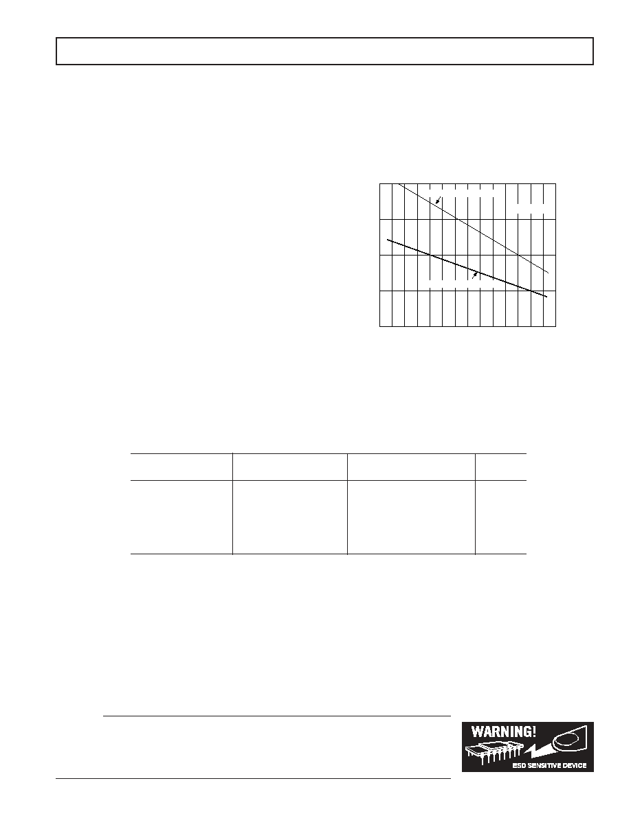
MAXIMUM POWER DISSIPATION (W)
AMBIENT TEMPERATURE ( C)
2.0
1.5
0
≠50
90
≠40 ≠30 ≠20 ≠10 0
10
20 30
50
60 70
80
40
1.0
0.5
8-LEAD PDIP PACKAGE
8-LEAD SOIC PACKAGE
T
J
= 150 C
Figure 3. Maximum Power Dissipation vs. Temperature
ORDERING GUIDE
Temperature
Package
Package
Model
Range
Description
Options
AD8041AN
≠40
∞C to +85∞C
8-Lead PDIP
N-8
AD8041AR
≠40
∞C to +85∞C
8-Lead Plastic SOIC
R-8
AD8041AR-REEL
≠40
∞C to +85∞C
13" Tape and Reel
R-8
AD8041AR-REEL7
≠40
∞C to +85∞C
7" Tape and Reel
R-8
AD8041ARZ-REEL
1
≠40
∞C to +85∞C
13" Tape and Reel
R-8
5962-9683901MPA
2
≠55
∞C to +125∞C
8-Lead CERDIP
Q-8
NOTES
1
The Z indicates a lead-free product.
2
Refer to official DSCC drawing for tested specifications.
CAUTION
ESD (electrostatic discharge) sensitive device. Electrostatic charges as high as 4000 V readily
accumulate on the human body and test equipment and can discharge without detection. Although the
AD8041 features proprietary ESD protection circuitry, permanent damage may occur on devices
subjected to high energy electrostatic discharges. Therefore, proper ESD precautions are recommended
to avoid performance degradation or loss of functionality.