
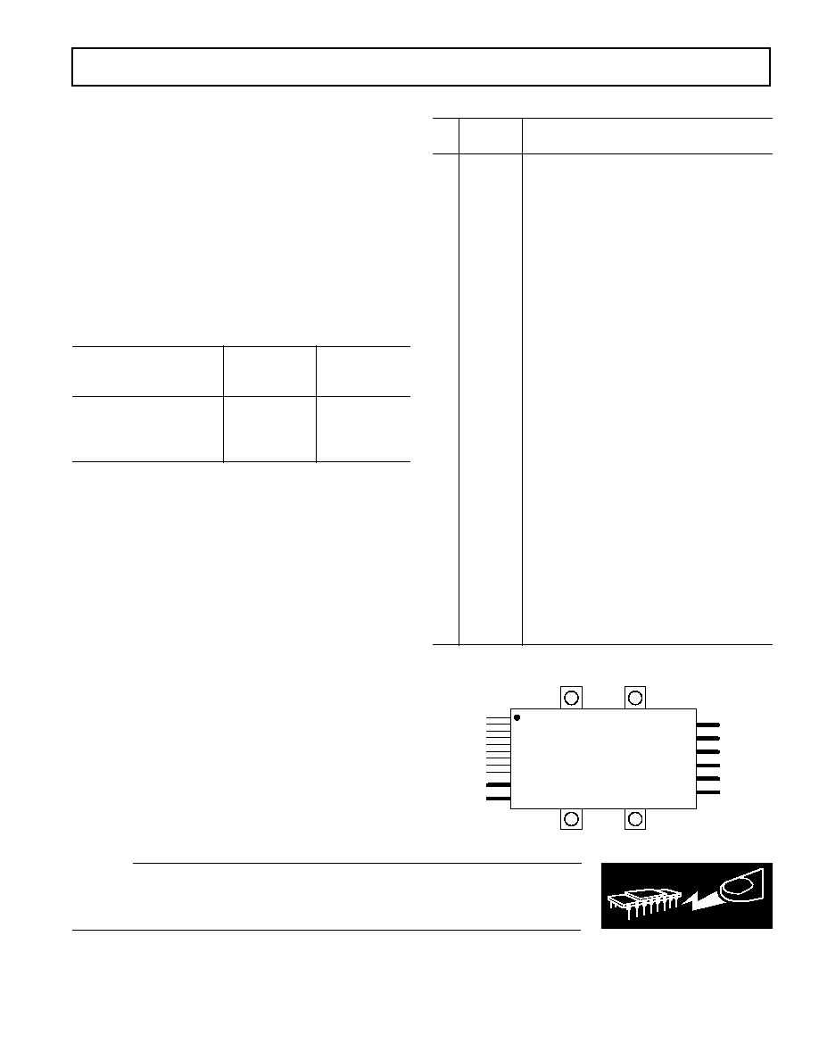
FUNCTIONAL BLOCK DIAGRAM
+V
OUT
RETURN
≠V
IN
+V
IN
RETURN
RETURN
+V
OUT
+V
OUT
ADJUST
STATUS
V
AUX
INHIBIT
SYNC
I
SHARE
TEMP
FIXED
FREQUENCY
DUAL
INTERLEAVED
POWER TRAIN
+SENSE
OUTPUT
FILTER
INPUT SIDE
CONTROL
CIRCUIT
EMI FILTER
ADDC02808PB
≠SENSE
OUTPUT SIDE
CONTROL
CIRCUIT
REV. A
Information furnished by Analog Devices is believed to be accurate and
reliable. However, no responsibility is assumed by Analog Devices for its
use, nor for any infringements of patents or other rights of third parties
which may result from its use. No license is granted by implication or
otherwise under any patent or patent rights of Analog Devices.
a
ADDC02808PB
FEATURES
28 V dc Input, 8 V dc @ 25 A, 200 W Pulse Output
Integral EMI Filter
Ultrafast Transient Response
Minimal Output Voltage Deviation
Low Weight: 80 Grams
NAVMAT Derated
Many Protection and System Features
APPLICATIONS
Distributed Power Architecture for Driving T/R Modules
Motor and Actuator Drivers
GENERAL DESCRIPTION
The ADDC02808PB hybrid military dc/dc converter is com-
pensated specifically for pulse applications where fast transient
response and minimum output voltage deviation are required.
It is also designed to deliver very high, pulsed output power.
The unit is designed for high reliability and high performance
applications where saving space and/or weight are critical.
The ADDC02808PB has been characterized over a wide variety
of load conditions. Its transient response has been set to insure
output stability over a broad range of load capacitance. For
applications that require factory modified compensation
optimized for a specific load, or for applications that require a
different output voltage than 8 V dc, contact the factory.
The ADDC02808PB is available in a hermetically sealed,
molybdenum based hybrid package and is easily heatsink
mountable. Three screening levels are available, including
military SMD.
28 V, 200 W Pulsed DC/DC Converter
with Integral EMI Filter
PRODUCT HIGHLIGHTS
1. 120 W/cubic inch pulsed power density with an integral EMI
filter
2. Ultrafast transient response time with minimum output
voltage deviation
3. Light weight: 85 grams
4. Operational and survivable over a wide range of input condi-
tions: 16 V≠50 V dc; survives low line, high line
5. High reliability; NAVMAT derated
6. Protection features include:
Output Overvoltage Protection
Output Short Circuit Current Protection
Thermal Monitor/Shutdown
Input Overvoltage Shutdown
Input Transient Protection
7. System level features include:
Current Sharing for Parallel Operation
Logic Level Disable
Output Status Signal
Synchronization for Multiple Units
Input Referenced Auxiliary Voltage Supply
One Technology Way, P.O. Box 9106, Norwood, MA 02062-9106, U.S.A.
Tel: 781/329-4700
World Wide Web Site: http://www.analog.com
Fax: 781/326-8703
© Analog Devices, Inc., 1998

ADDC02808PB≠SPECIFICATIONS
ELECTRICAL CHARACTERISTICS
Case
Test
ADDC02808PB
Parameter
Temp
Level
Conditions
Min
Typ
Max
Units
INPUT CHARACTERISTICS
Steady State Operating Input Voltage Range
1
Full
VI
I
O
= 1.25 A to 25 A Pulsed
18
28
40
V
Abnormal Operating Input Voltage Range
(Per MIL-STD-704D)
1
Full
VI
I
O
= 1.25 A to 25 A Pulsed
16
50
V
Input Overvoltage Shutdown
+25
∞
C
I
50
52.5
55
V
No Load Input Current
+25
∞
C
VI
45
90
mA
Disabled Input Current
+25
∞
C
VI
1
2
mA
OUTPUT CHARACTERISTICS
2, 3
Output Voltage (V
O
)
+25
∞
C
I
I
O
= 1.25 A to 25 A, V
IN
= 18 V to 40 V dc
7.92
8.00
8.08
V
Full
VI
I
O
= 1.25 A to 25 A, V
IN
= 18 V to 40 V dc
7.84
8.16
V
Full
VI
I
O
= 1.25 A to 20 A, V
IN
= 16 V to 50 V dc
7.84
8.16
V
Line Regulation
+25
∞
C
VI
I
O
= 25 A Pulsed, V
IN
= 18 V to 40 V dc
1
5
mV
Load Regulation
+25
∞
C
VI
V
IN
= 28 V dc, I
O
= 1.25 A to 25 A Pulsed
2.5
10
mV
Output Ripple/Noise
4
+25
∞
C
I
I
O
= 25 A, 5 kHz ≠ 2 MHz BW
10
30
mV p-p
Output Current (I
O
)
5
Full
VI
V
IN
= 18 V to 40 V dc, Pulsed
1.25
25
A
Output Overvoltage Protection
+25
∞
C
V
I
O
= 25 A, Open Remote Sense Connection
125
% V
O
nom
Output Current Limit
+25
∞
C
V
V
O
= 90% V
OUT
Nom
130
% I
O
max
Output Short Circuit Current
+25
∞
C
I
40
A
ISOLATION CHARACTERISTICS
Isolation Resistance
+25
∞
C
I
Input to Output or Any Pin to Case at 500 V dc
100
M
DYNAMIC CHARACTERISTICS
4
Step Changes In Load (min to max)
+25
∞
C
I
(Reference Section Entitled "Transient Response")
Step Changes In Load (max to min)
(Reference Section Entitled "Response at End
of Pulse")
Soft Start Turn-On Time
+25
∞
C
I
I
O
= 25 A, From Inhibit High to Status High
6
10
ms
THERMAL CHARACTERISTICS
Efficiency
+25
∞
C
I
I
O
= 12.5 A
77.5
Min
VI
I
O
= 12.5 A
77.5
80
%
Max
VI
I
O
= 12.5 A
76
%
+25
∞
C
I
I
O
= 25 A
73.5
76
%
Min
VI
I
O
= 25 A
73.5
%
Max
VI
I
O
= 25 A
71
%
Hottest Junction Temperature
5
+90
∞
C
V
I
O
= 25 A
110
∞
C
CONTROL CHARACTERISTICS
Clock Frequency
Full
VI
I
O
= 2 A
0.85
0.99
MHz
ADJUST (Pin 3) V ADJ
+25
∞
C
I
3.1
3.2
3.3
V
STATUS (Pin 4)
V
OH
+25
∞
C
I
I
OH
= 400
µ
A
2.4
4.0
V
V
OL
+25
∞
C
I
I
OL
= 1 mA
0.15
0.7
V
V
AUX
(Pin 5)
V
O
(nom)
+25
∞
C
I
I
AUX
= 5 mA, Load Current = 12.5 A
14.65 15.15
15.65
V
INHIBIT (Pin 6)
V
IL
+25
∞
C
I
0.5
V
I
IL
+25
∞
C
I
V
IL
= 0.5 V
1.2
mA
V
I
(Open Circuit)
+25
∞
C
I
15
V
SYNC (Pin 7)
6
V
IH
+25
∞
C
I
4.0
V
I
IH
+25
∞
C
I
V
IH
= 7.0 V
175
µ
A
I
SHARE
(Pin 8)
+25
∞
C
I
I
O
= 20 A
2.45
2.55
2.65
V
TEMP (Pin 9)
+25
∞
C
V
3.90
V
NOTES
1
50 V dc upper limit rated for transient condition of up to 50 ms. 16 V dc lower limit rated for continuous operation during emergency condition. Steady state and
abnormal input voltage range require source impedance sufficient to insure input stability at low line. See sections entitled System Instability Considerations and Input
Voltage Range.
2
Measured at the remote sense points.
3
Unit regulates output voltage to zero load; tests performed at low continuous load and 200 W pulsed load.
4
C
LOAD
= 1,000
µ
F. Output ripple/noise measured at converter output; may be smaller at external load capacitance. Unit is stable for C
LOAD
ranging from 500
µ
F to
4,000
µ
F.
5
Refer to section entitled "Pulse Output Power vs. Pulse Length" for more information.
6
Unit has internal pull-down; refer to section entitled Pin 7 (SYNC).
Specifications subject to change without notice.
REV. A
≠2≠
(T
C
= +25 C, V
IN
= 28 V dc 0.5 V dc, unless otherwise noted; full temperature range is
≠55 C to +90 C; all temperatures are case and T
C
is the temperature measured at the center of the package bottom.)
ADDC02808PB
REV. A
≠3≠
CAUTION
ESD (electrostatic discharge) sensitive device. Electrostatic charges as high as 4000 V readily
accumulate on the human body and test equipment and can discharge without detection.
Therefore, proper ESD precautions are recommended to avoid performance degradation or loss
of functionality.
ABSOLUTE MAXIMUM RATINGS*
INHIBIT . . . . . . . . . . . . . . . . . . . . . . . . . . 50 V dc, ≠0.5 V dc
SYNC . . . . . . . . . . . . . . . . . . . . . . . . . . . . 8.0 V dc, ≠0.5 V dc
I
SHARE
. . . . . . . . . . . . . . . . . . . . . . . . . . . . . 6 V dc, ≠0.5 V dc
TEMP . . . . . . . . . . . . . . . . . . . . . . . . . . . . 12 V dc, ≠0.3 V dc
Common-Mode Voltage, Input to Output . . . . . . . . . 500 V dc
Lead Soldering Temp (10 sec) . . . . . . . . . . . . . . . . . . . +300
∞
C
Storage Temperature . . . . . . . . . . . . . . . . . . ≠65
∞
C to +150
∞
C
Maximum Junction Temperature . . . . . . . . . . . . . . . . +150
∞
C
Maximum Case Operating Temperature . . . . . . . . . . . +125
∞
C
*Absolute maximum ratings are limiting values, to be applied individually, and
beyond which the serviceability of the circuit may be impaired. Functional
operability under any of these conditions is not necessarily implied. Exposure of
absolute maximum rating conditions for extended periods of time may affect
device reliability.
ORDERING GUIDE
Operating
Temperature
Device
Range (Case)
Description
ADDC02808PBKV
≠40
∞
C to +85
∞
C
Hermetic Package
ADDC02808PBTV
≠55
∞
C to +90
∞
C
Hermetic Package
5962-9763401HXC
≠55
∞
C to +125
∞
C Hermetic Package
(ADDC02808PBTV/QMLH)
EXPLANATION OF TEST LEVELS
Test Level
I
≠
100% production tested.
II
≠
100% production tested at +25
∞
C, and sample tested at
specified temperatures.
III ≠
Sample tested only.
IV ≠
Parameter is guaranteed by design and characterization
testing.
V
≠
Parameter is a typical value only.
VI ≠
All devices are 100% production tested at +25
∞
C. 100%
production tested at temperature extremes for military
temperature devices; guaranteed by design and charac-
terization testing for industrial devices.
PIN FUNCTION DESCRIPTIONS
Pin
No.
Name
Function
1
≠SENSE
Feedback loop connection for remote sensing
output voltage. Must always be connected to
output return for proper operation.
2
+SENSE
Feedback loop connection for remote sensing
output voltage. Must always be connected to
+V
OUT
for proper operation.
3
ADJUST
Adjusts output voltage setpoint.
4
STATUS
Indicates output voltage is within
±
5% of
nominal. Active high referenced to ≠SENSE
(Pin 1).
5
V
AUX
Low level dc auxiliary voltage supply refer-
enced to input return (Pin 10).
6
INHIBIT
Power Supply Inhibit. Active low and refer-
enced to input return (Pin 10).
7
SYNC
Clock synchronization input for multiple
units; referenced to input return (Pin 10).
8
I
SHARE
Current share pin which allows paralleled
units to share current typically within
±
5% at
full load; referenced to input return (Pin 10).
9
TEMP
Case temperature indicator and temperature
shutdown override; referenced to input return
(Pin 10).
10
≠V
IN
Input Return.
11
+V
IN
+28 V Nominal Input Bus.
12
+V
OUT
+8 V dc Output.
13
+V
OUT
+8 V dc Output.
14
+V
OUT
+8 V dc Output.
15
RETURN Output Return.
16
RETURN Output Return.
17
RETURN Output Return.
PIN CONFIGURATION
1
11
12
17
TOP
VIEW
WARNING!
ESD SENSITIVE DEVICE

ADDC02808PB≠Typical Performance Curves
REV. A
≠4≠
OUTPUT POWER ≠ Watts
82
68
0
20
PERCENTAGE
40
60
80
100
80
78
76
120
140
160
180
200
74
72
70
40V
28V
18V
Figure 1. Efficiency vs. Line and Load at +25
∞
C
(Load Pulsewidth of 50 ms)
T
CASE
79
79
76
≠55
95
≠45
EFFICIENCY ≠ Percentage
≠35 ≠25 ≠15 ≠5
78
78
77
77
5
15
25 35
45 55 65
75 85
28V
IN
, 150W PEAK
Figure 2. Efficiency vs. Case Temperature (
∞
C)
(at Nominal V
IN
, 75% Max Load, Load Pulsewidth
of 50 ms)
PEAK OUTPUT POWER ≠ Watts
16.0
15.5
13.0
140
200
150
INPUT VOLTAGE
160
170
180
190
15.0
14.5
13.5
14.0
Figure 3. Low Line Dropout vs. Load at 90
∞
C Case
Temperature (Load Pulsewidth of 50 ms)
T
CASE
1.0
≠1.0
≠55
95
≠45 ≠35 ≠25 ≠15 ≠5
0.5
0.0
≠0.5
5
15
25 35
45 55 65
75 85
28V
IN
, 150W PEAK
V
OUT
DEVIATION ≠ %
Figure 4. Output Voltage vs. Case Temperature (
∞
C)
2V
10V
10
0%
100
90
1ms
V
O
V
INHIBIT
Figure 5. Output Voltage Transient During Turn-On with
0.1 A Load Displaying Soft Start When Supply Is Enabled
100mV
10
0%
100
90
100 s
V
O
Figure 6. Output Voltage Transient Response to
a 1 A to 25 A Step Change in Load, di/dt = 12 A/
µ
s,
with 1,000
µ
F Load Capacitance (R
ESR
= 10 m
)
ADDC02808PB
REV. A
≠5≠
FREQUENCY ≠ Hz
0
≠10
≠100
10
50k
100
|AS| ≠ dB
1k
10k
≠20
≠30
≠40
≠50
≠60
≠70
≠80
≠90
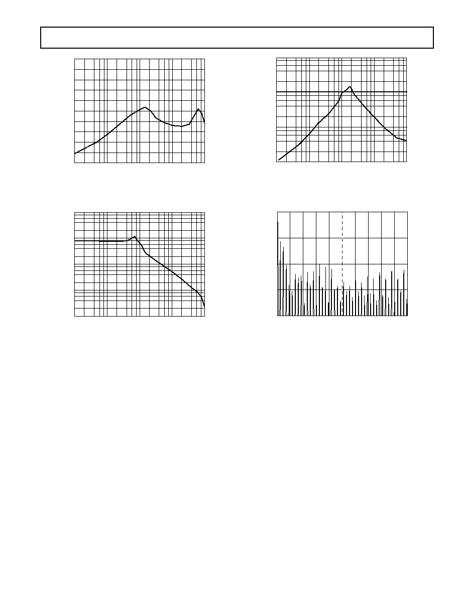
Figure 7. Audio Susceptibility (Magnitude of V
OUT
/V
IN
)
1k
0.1
|Z
IN
| ≠
100
10
1
FREQUENCY ≠ Hz
10
100k
100
1k
10k
Figure 8. Incremental Input Impedance (Magnitude)
1
0.001
|Z
OUT
| ≠
0.1
0.01
FREQUENCY ≠ Hz
10
100k
100
1k
10k
Figure 9. Incremental Output Impedance (Magnitude)
5mV
1mV
50 V
0
20
VOLTS
10
0.5mV
100 V
FREQUENCY ≠ MHz
Figure 10. Output Frequency Spectrum