 | –≠–ª–µ–∫—Ç—Ä–æ–Ω–Ω—ã–π –∫–æ–º–ø–æ–Ω–µ–Ω—Ç: 7812 | –°–∫–∞—á–∞—Ç—å:  PDF PDF  ZIP ZIP |
Information furnished by Analog Devices is believed to be accurate and
reliable. However, no responsibility is assumed by Analog Devices for its
use, nor for any infringements of patents or other rights of third parties
which may result from its use. No license is granted by implication or
otherwise under any patent or patent rights of Analog Devices.
a
AD7811/AD7812
One Technology Way, P.O. Box 9106, Norwood, MA 02062-9106, U.S.A.
Tel: 781/329-4700
World Wide Web Site: http://www.analog.com
Fax: 781/326-8703
© Analog Devices, Inc., 2000
2.7 V to 5.5 V, 350 kSPS, 10-Bit
4-/8-Channel Sampling ADCs
FEATURES
10-Bit ADC with 2.3 s Conversion Time
The AD7811 has Four Single-Ended Inputs that
Can Be Configured as Three Pseudo Differential
Inputs with Respect to a Common, or as Two Inde-
pendent Pseudo Differential Channels
The AD7812 has Eight Single-Ended Inputs that Can
Be Configured as Seven Pseudo Differential Inputs
with Respect to a Common, or as Four Independent
Pseudo Differential Channels
Onboard Track and Hold
Onboard Reference 2.5 V 2.5%
Operating Supply Range: 2.7 V to 5.5 V
Specifications at 2.7 V≠3.6 V and 5 V 10%
DSP-/Microcontroller-Compatible Serial Interface
High Speed Sampling and Automatic Power-Down Modes
Package Address Pin on the AD7811 and AD7812 Allows
Sharing of the Serial Bus in Multipackage Applications
Input Signal Range: 0 V to V
REF
Reference Input Range: 1.2 V to V
DD
GENERAL DESCRIPTION
The AD7811 and AD7812 are high speed, low power, 10-bit
A/D converters that operate from a single 2.7 V to 5.5 V supply.
The devices contain a 2.3
µs successive approximation A/D
converter, an on-chip track/hold amplifier, a 2.5 V on-chip refer-
ence and a high speed serial interface that is compatible with the
serial interfaces of most DSPs (Digital Signal Processors) and
microcontrollers. The user also has the option of using an exter-
nal reference by connecting it to the V
REF
pin and setting the
EXTREF bit in the control register. The V
REF
pin may be tied
to V
DD
. At slower throughput rates the power-down mode may
be used to automatically power down between conversions.
The control registers of the AD7811 and AD7812 allow the
input channels to be configured as single-ended or pseudo
differential. The control register also features a software convert
start and a software power-down. Two of these devices can
share the same serial bus and may be individually addressed in
a multipackage application by hardwiring the device address pin.
The AD7811 is available in a small, 16-lead 0.3" wide, plastic
dual-in-line package (mini-DIP), in a 16-lead 0.15" wide, Small
Outline IC (SOIC) and in a 16-lead, Thin Shrink Small Out-
line Package (TSSOP). The AD7812 is available in a small,
20-lead 0.3" wide, plastic dual-in-line package (mini-DIP), in a
20-lead, Small Outline IC (SOIC) and in a 20-lead, Thin Shrink
Small Outline Package (TSSOP).
PRODUCT HIGHLIGHTS
1. Low Power, Single Supply Operation
Both the AD7811 and AD7812 operate from a single 2.7 V
to 5.5 V supply and typically consume only 10 mW of power.
The power dissipation can be significantly reduced at
lower throughput rates by using the automatic power-
down mode e.g., 315
µW @ 10 kSPS, V
DD
= 3 V--see
Power vs. Throughput.
2. 4-/8-Channel, 10-Bit ADC
The AD7811 and AD7812 have four and eight single-ended
input channels respectively. These inputs can be configured
as pseudo differential inputs by using the Control Register.
3. On-chip 2.5 V (
±2.5%) reference circuit that is powered
down when using an external reference.
4. Hardware and Software Control
The AD7811 and AD7812 provide for both hardware and
software control of Convert Start and Power-Down.
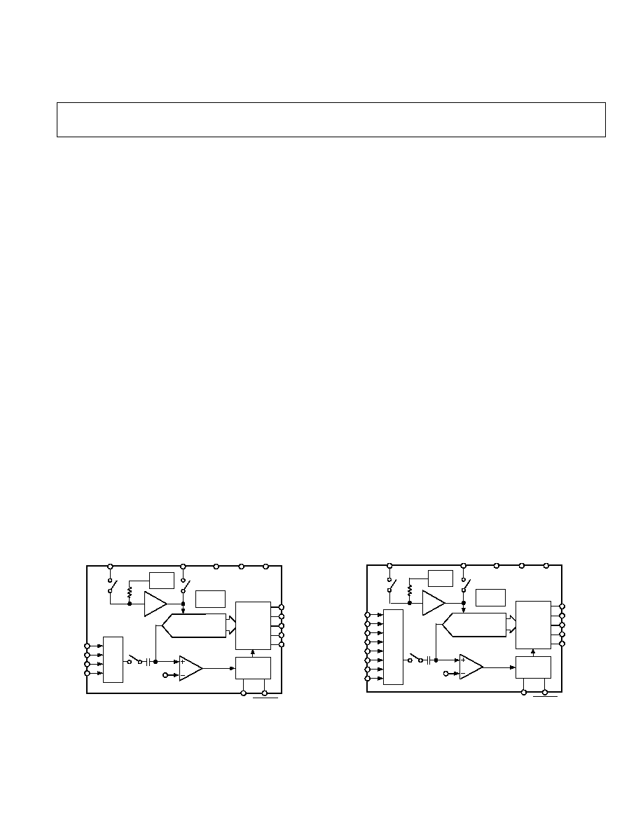
FUNCTIONAL BLOCK DIAGRAMS
REV. B
CHARGE
REDISTRIBUTION
DAC
CLOCK
OSC
AD7811
CONVST
AGND
V
DD
/3
COMP
REF
IN
V
DD
DOUT
DGND
A0
V
IN1
V
IN2
V
IN3
V
IN4
DIN
RFS
TFS
SCLK
BUF
CONTROL
LOGIC
MUX
C
REF
SERIAL
PORT
1.23V
REF
CHARGE
REDISTRIBUTION
DAC
CLOCK
OSC
AD7812
AGND
REF
IN
V
DD
DOUT
DGND
A0
DIN
RFS
TFS
SCLK
BUF
CONTROL
LOGIC
MUX
C
REF
SERIAL
PORT
V
IN1
V
IN2
V
IN3
V
IN4
V
IN5
V
IN6
V
IN7
V
IN8
CONVST
V
DD
/3
COMP
1.23V
REF

≠2≠
REV. B
AD7811/AD7812≠SPECIFICATIONS
Parameter
Y Version
Unit
Test Conditions/Comments
DYNAMIC PERFORMANCE
f
IN
= 30 kHz Any Channel, f
SAMPLE
= 350 kHz
Signal to (Noise + Distortion) Ratio
1
58
dB min
V
REF
Internal or External
Total Harmonic Distortion (THD)
1
≠66
dB max
Peak Harmonic or Spurious Noise
1
≠80
dB typ
Intermodulation Distortion
1, 2
fa = 29 kHz, fb = 30 kHz
Second Order Terms
≠67
dB max
Third Order Terms
≠67
dB max
Channel-to-Channel Isolation
1, 2
≠80
dB typ
f
IN
= 20 kHz
DC ACCURACY
Any Channel
Resolution
10
Bits
Minimum Resolution for Which
No Missing Codes are Guaranteed
10
Bits
Relative Accuracy
1
±1
LSB max
Differential Nonlinearity
1
±1
LSB max
Gain Error
1
±2
LSB max
Gain Error Match
1
±0.75
LSB max
Offset Error
1
±2
LSB max
Offset Error Match
1
±0.75
LSB max
ANALOG INPUT
Input Voltage Range
0
V min
V
REF
V max
Input Leakage Current
2
±1
µA max
Input Capacitance
2
20
pF max
REFERENCE INPUTS
2
V
REF
Input Voltage Range
1.2
V min
V
DD
V max
Input Leakage Current
±3
µA max
Input Capacitance
20
pF max
ON-CHIP REFERENCE
Nominal 2.5 V
Reference Error
±2.5
% max
Temperature Coefficient
50
ppm/
∞C typ
LOGIC INPUTS
2
V
INH
,
Input High Voltage
2.4
V min
V
DD
= 5 V
± 10%
V
INL
, Input Low Voltage
0.8
V max
V
DD
= 5 V
± 10%
V
INH
,
Input High Voltage
2
V min
V
DD
= 3 V
± 10%
V
INL
, Input Low Voltage
0.4
V max
V
DD
= 3 V
± 10%
Input Current, I
IN
±1
µA max
Typically 10 nA, V
IN
= 0 V to V
DD
Input Capacitance, C
IN
8
pF max
LOGIC OUTPUTS
Output High Voltage, V
OH
I
SOURCE
= 200
µA
4
V min
V
DD
= 5 V
± 10%
2.4
V min
V
DD
= 3 V
± 10%
Output Low Voltage, V
OL
I
SINK
= 200
µA
0.4
V max
High Impedance Leakage Current
±1
µA max
High Impedance Capacitance
15
pF max
CONVERSION RATE
Conversion time
2.3
µs max
Track/Hold Acquisition Time
1
200
ns max
(V
DD
= 2.7 V to 3.6 V, V
DD
= 5 V 10%, GND = 0 V, V
REF
= V
DD
[EXT]. All specifications ≠40 C to +105 C
unless otherwise noted.)
≠3≠
REV. B
AD7811/AD7812
Parameter
Y Version
Unit
Test Conditions/Comments
POWER SUPPLY
V
DD
2.7
V min
For Specified Performance
5.5
V max
I
DD
Digital Inputs = 0 V or V
DD
Normal Operation
3.5
mA max
Power-Down
Full Power-Down
1
µA max
Partial Power-Down (Internal Ref)
350
µA max
See Power-Up Times Section
Power Dissipation
V
DD
= 3 V
Normal Operation
10.5
mW max
Auto Full Power-Down
See Power vs. Throughput Section
Throughput 1 kSPS
31.5
µW max
Throughput 10 kSPS
315
µW max
Throughput 100 kSPS
3.15
mW max
Partial Power-Down (Internal Ref)
1.05
mW max
Full Power-Down
3
µW max
NOTES
1
See Terminology.
2
Sample tested during initial release and after any redesign or process change that may affect this parameter.
Specifications subject to change without notice.
TIMING CHARACTERISTICS
1, 2
Parameter
Y Version
Unit
Conditions/Comments
t
POWER-UP
1.5
µs (max)
Power-Up Time of AD7811/AD7812 after Rising Edge of
CONVST
t
1
2.3
µs (max)
Conversion Time
t
2
20
ns (min)
CONVST Pulsewidth
t
3
25
ns (min)
SCLK High Pulsewidth
t
4
25
ns (min)
SCLK Low Pulsewidth
t
5
3
5
ns (min)
RFS Rising Edge to SCLK Rising Edge Setup Time
t
6
3
5
ns (min)
TFS Falling Edge to SCLK Falling Edge Setup Time
t
7
3
10
ns (max)
SCLK Rising Edge to Data Out Valid
t
8
10
ns (min)
DIN Data Valid to SCLK Falling Edge Setup Time
t
9
5
ns (min)
DIN Data Valid after SCLK Falling Edge Hold Time
t
10
3, 4
20
ns (max)
SCLK Rising Edge to D
OUT
High Impedance
t
11
100
ns (min)
DOUT High Impedance to
CONVST Falling Edge
NOTES
1
Sample tested to ensure compliance.
2
See Figures 16, 17 and 18.
3
These numbers are measured with the load circuit of Figure 1. They are defined as the time required for the o/p to cross 0.8 V or 2.4 V for V
DD
= 5 V
± 10% and
0.4 V or 2 V for V
DD
= 3 V
± 10%.
4
Derived from the measured time taken by the data outputs to change 0.5 V when loaded with the circuit of Figure 1. The measured number is then extrapolated back
to remove the effects of charging or discharging the 50 pF capacitor. This means that the time, t
11
, quoted in the Timing Characteristics is the true bus relinquish
time of the part and as such is independent of external bus loading capacitances.
Specifications subject to change without notice.
(V
DD
= 2.7 V to 5.5 V, V
REF
= V
DD
[EXT] unless otherwise noted)
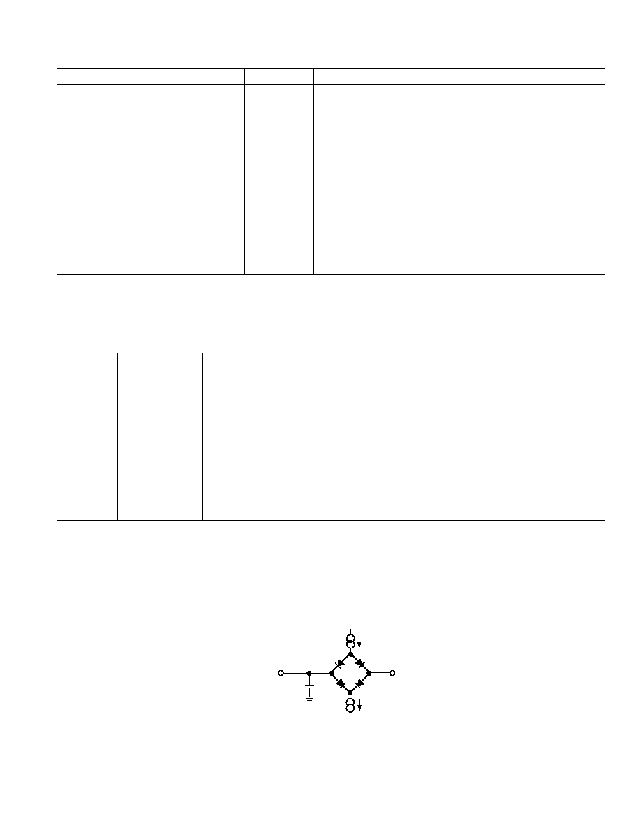
2.1V
200 A
C
L
50pF
I
OH
TO
OUTPUT
PIN
I
OL
200 A
Figure 1. Load Circuit for Digital Output Timing Specifications

AD7811/AD7812
≠4≠
REV. B
ABSOLUTE MAXIMUM RATINGS
*
V
DD
to DGND . . . . . . . . . . . . . . . . . . . . . . . . . ≠0.3 V to +7 V
Digital Input Voltage to DGND (
CONVST, SCLK, RFS, TFS,
DIN, A0) . . . . . . . . . . . . . . . . . . . . . . . ≠0.3 V, V
DD
+ 0.3 V
Digital Output Voltage to DGND (DOUT)
. . . . . . . . . . . . . . . . . . . . . . . . . . . . . . . ≠0.3 V, V
DD
+ 0.3 V
REF
IN
to AGND . . . . . . . . . . . . . . . . . . . ≠0.3 V, V
DD
+ 0.3 V
Analog Inputs
V
IN1
≠V
IN4
(AD7811) . . . . . . . . . . . . . . ≠0.3 V, V
DD
+ 0.3 V
V
IN1
≠V
IN8
(AD7812) . . . . . . . . . . . . . . ≠0.3 V, V
DD
+ 0.3 V
Storage Temperature Range . . . . . . . . . . . . ≠65
∞C to +150∞C
Junction Temperature . . . . . . . . . . . . . . . . . . . . . . . . . . 150
∞C
Plastic DIP Package, Power Dissipation . . . . . . . . . . 450 mW
JA
Thermal Impedance . . . . . . . . . . . . . . . . . . . . 105
∞C/W
Lead Temperature, (Soldering 10 sec) . . . . . . . . . . . . 260
∞C
ORDERING GUIDE
Linearity
Package
Package
Model
Error
Descriptions
Options
AD7811YN
±1 LSB
16-Lead Plastic DIP
N-16
AD7811YR
±1 LSB
16-Lead Small Outline IC (SOIC)
R-16A
AD7811YRU
±1 LSB
16-Lead Thin Shrink Small Outline Package (TSSOP)
RU-16
AD7812YN
±1 LSB
20-Lead Plastic DIP
N-20
AD7812YR
±1 LSB
20-Lead Small Outline IC (SOIC)
R-20A
AD7812YRU
±1 LSB
20-Lead Thin Shrink Small Outline Package (TSSOP)
RU-20
SOIC Package, Power Dissipation . . . . . . . . . . . . . . . 450 mW
JA
Thermal Impedance . . . . . . . . . . . . . . . . . . . . . 75
∞C/W
Lead Temperature, Soldering
Vapor Phase (60 sec) . . . . . . . . . . . . . . . . . . . . . . . 215
∞C
Infrared (15 sec) . . . . . . . . . . . . . . . . . . . . . . . . . . 220
∞C
TSSOP Package, Power Dissipation . . . . . . . . . . . . . 450 mW
JA
Thermal Impedance . . . . . . . . . . . . . . . . . . . . 115
∞C/W
Lead Temperature, Soldering
Vapor Phase (60 sec) . . . . . . . . . . . . . . . . . . . . . . . 215
∞C
Infrared (15 sec) . . . . . . . . . . . . . . . . . . . . . . . . . . 220
∞C
*Stresses above those listed under Absolute Maximum Ratings may cause perma-
nent damage to the device. This is a stress rating only; functional operation of the
device at these or any other conditions above those listed in the operational
sections of this specification is not implied. Exposure to absolute maximum rating
conditions for extended periods may affect device reliability.
CAUTION
ESD (electrostatic discharge) sensitive device. Electrostatic charges as high as 4000 V readily
accumulate on the human body and test equipment and can discharge without detection. Although
the AD7811/AD7812 features proprietary ESD protection circuitry, permanent damage may occur
on devices subjected to high-energy electrostatic discharges. Therefore, proper ESD precautions
are recommended to avoid performance degradation or loss of functionality.
WARNING!
ESD SENSITIVE DEVICE
AD7811/AD7812
≠5≠
REV. B
PIN FUNCTION DESCRIPTIONS
Pin(s)
Pin(s)
AD7811
AD7812
Mnemonic
Description
1
1
V
REF
An external reference input can be applied here. When using an external precision
reference or V
DD
the EXTREF bit in the control register must be set to logic one. The
external reference input range is 1.2 V to V
DD
.
2
2
C
REF
Reference Capacitor. A capacitor (10 nF) is connected here to improve the noise
performance of the on-chip reference.
3, 5≠7
3, 5≠11
V
IN1
≠V
IN4(8)
Analog Inputs. The analog input range is 0 V to V
REF
.
4
4
AGND
Analog Ground. Ground reference for track/hold, comparator, on-chip reference and
DAC.
8
12
A0
Package Address Pin. This Logic Input can be hardwired high or low. When used in
conjunction with the package address bit in the control register this input allows two
devices to share the same serial bus. For example a twelve channel solution can be
achieved by using the AD7811 and the AD7812 on the same serial bus.
9
13
DGND
Digital Ground. Ground reference for digital circuitry.
10
14
TFS
Transmit Frame Sync. The falling edge of this Logic Input tells the part that a new
control byte should be shifted in on the next 10 falling edges of SCLK.
11
15
RFS
Receive Frame Sync. The rising edge of this Logic Input is used to enable a counter in
the serial interface. It is used to provide compatibility with DSPs which use a continuous
serial clock and framing signal. In multipackage applications the RFS Pin can also be
used as a serial bus select pin. The serial interface will ignore the SCLK until it receives a
rising edge on this input. The counter is reset at the end of a serial read operation.
12
16
DOUT
Serial Data Output. Serial data is shifted out on this pin on the rising edge of the serial
clock. The output enters a High impedance condition on the rising edge of the 11th
SCLK pulse.
13
17
DIN
Serial Data Input. The control byte is read in at this input. In order to complete a
serial write operation 13 SCLK pulses need to be provided. Only the first 10 bits are
shifted in--see Serial Interface section.
14
18
SCLK
Serial Clock Input. An external serial clock is applied to this input to obtain serial data
from the AD7811/AD7812 and also to latch data into the AD7811/AD7812. Data is
clocked out on the rising edge of SCLK and latched in on the falling edge of SCLK.
15
19
CONVST
Convert Start. This is an edge triggered logic input. The Track/Hold goes into its Hold
Mode on the falling edge of this signal and a conversion is initiated. The state of this
pin at the end of conversion also determines whether the part is powered down or not.
See operating modes section of this data sheet.
16
20
V
DD
Positive Supply Voltage 2.7 V to 5.5 V.
PIN CONFIGURATIONS
DIP/SOIC/TSSOP
14
13
12
11
16
15
10
9
8
1
2
3
4
7
6
5
TOP VIEW
(Not to Scale)
AD7811
V
REF
DIN
SCLK
CONVST
V
DD
C
REF
V
IN1
AGND
TFS
RFS
DOUT
V
IN2
V
IN3
V
IN4
A0
DGND
14
13
12
11
17
16
15
20
19
18
10
9
8
1
2
3
4
7
6
5
TOP VIEW
(Not to Scale)
AD7812
V
REF
DIN
SCLK
V
DD
C
REF
V
IN1
AGND
TFS
RFS
DOUT
V
IN2
V
IN3
V
IN4
V
IN5
V
IN6
V
IN7
V
IN8
A0
DGND
CONVST

AD7811/AD7812
≠6≠
REV. B
TERMINOLOGY
Signal to (Noise + Distortion) Ratio
This is the measured ratio of signal to (noise + distortion) at the
output of the A/D converter. The signal is the rms amplitude of
the fundamental. Noise is the rms sum of all nonfundamental
signals up to half the sampling frequency (f
S
/2), excluding dc.
The ratio is dependent upon the number of quantization levels
in the digitization process; the more levels, the smaller the
quantization noise. The theoretical signal to (noise + distor-
tion) ratio for an ideal N-bit converter with a sine wave input
is given by:
Signal to (Noise + Distortion) = (6.02N + 1.76) dB
Thus for a 10-bit converter, this is 62 dB.
Total Harmonic Distortion
Total harmonic distortion (THD) is the ratio of the rms sum of
harmonics to the fundamental. For the AD7811 and AD7812
it is defined as:
THD (dB)
= 20 log
V
2
2
+V
3
2
+V
4
2
+V
5
2
+V
6
2
V
1
where V
1
is the rms amplitude of the fundamental and V
2
, V
3
,
V
4
, V
5
and V
6
are the rms amplitudes of the second through the
sixth harmonics.
Peak Harmonic or Spurious Noise
Peak harmonic or spurious noise is defined as the ratio of the
rms value of the next largest component in the ADC output
spectrum (up to f
S
/2 and excluding dc) to the rms value of the
fundamental. Normally, the value of this specification is
determined by the largest harmonic in the spectrum, but for
parts where the harmonics are buried in the noise floor, it will
be a noise peak.
Intermodulation Distortion
With inputs consisting of sine waves at two frequencies, fa and
fb, any active device with nonlinearities will create distortion
products at sum and difference frequencies of mfa
± nfb where
m, n = 0, 1, 2, 3, etc. Intermodulation terms are those for
which neither m nor n are equal to zero. For example, the
second order terms include (fa + fb) and (fa ≠ fb), while the
third order terms include (2fa + fb), (2fa ≠ fb), (fa + 2fb) and
(fa ≠ 2fb).
The AD7811 and AD7812 are tested using the CCIF standard
where two input frequencies near the top end of the input
bandwidth are used. In this case, the second and third order
terms are of different significance. The second order terms are
usually distanced in frequency from the original sine waves
while the third order terms are usually at a frequency close to
the input frequencies. As a result, the second and third order
terms are specified separately. The calculation of the inter-
modulation distortion is as per the THD specification where it is
the ratio of the rms sum of the individual distortion products to
the rms amplitude of the fundamental expressed in dBs.
Channel-to-Channel Isolation
Channel-to-channel isolation is a measure of the level of
crosstalk between channels. It is measured by applying a full-
scale 20 kHz sine wave signal to all nonselected input channels
and determining how much that signal is attenuated in the selected
channel. The figure given is the worst case across all four or
eight channels for the AD7811 and AD7812 respectively.
Relative Accuracy
Relative accuracy, or endpoint nonlinearity, is the maximum
deviation from a straight line passing through the endpoints of
the ADC transfer function.
Differential Nonlinearity
This is the difference between the measured and the ideal
1 LSB change between any two adjacent codes in the ADC.
Offset Error
This is the deviation of the first code transition (0000 . . . 000)
to (0000 . . . 001) from the ideal, i.e., AGND + 1 LSB.
Offset Error Match
This is the difference in Offset Error between any two channels.
Gain Error
This is the deviation of the last code transition (1111 . . . 110)
to (1111 . . . 111) from the ideal, i.e., V
REF
≠ 1 LSB, after the
offset error has been adjusted out.
Gain Error Match
This is the difference in Gain Error between any two channels.
Track/Hold Acquisition Time
Track/hold acquisition time is the time required for the output
of the track/hold amplifier to reach its final value, within
± 1/2 LSB, after the end of conversion (the point at which the
track/hold returns to track mode). It also applies to situations
where a change in the selected input channel takes place or
where there is a step input change on the input voltage applied
to the selected V
IN
input of the AD7811 or AD7812. It means
that the user must wait for the duration of the track/hold acquisi-
tion time after the end of conversion or after a channel change/
step input change to V
IN
before starting another conversion, to
ensure that the part operates to specification.

AD7811/AD7812
≠7≠
REV. B
Control Register (AD7811)
The Control Register is a 10-bit-wide, write only register. The Control Register is written to when the AD7811 receives a falling
edge on its TFS pin. The AD7811 will maintain the same configuration until a new control byte is written to the part. The control
register can be written to at the same time data is being read. This latter feature enhances throughput rates when software control is
being used or when the analog input channels are being changed frequently. The power-up default register contents are all zeros;
therefore, when the supplies are connected, the AD7811 is powered down by default.
Control Register AD7811
9
0
X
*
0
A
1
D
P
0
D
P
V
4
N
I
/
D
N
G
A
/
F
F
I
D
L
G
S
1
H
C
0
H
C
T
S
V
N
O
C
F
E
R
T
X
E
*This is a don't care bit.
A0
This is the package address bit. It is used in conjunction with the package address pin to allow two AD7811s to
share the same serial bus. The AD7811 can also share the same serial bus with the AD7812. When a control word
is written to the control register of the AD7811 the control word is ignored if the package address bit in the con-
trol byte does not match how the package address pin is hardwired. Only the serial port of the device that received
the last valid control byte, i.e., the address bit matched the address pin, will attempt to drive the serial bus on the
next serial read. When the part powers up this bit is set to 0.
PD1, PD0
These bits allow the AD7811 to be fully powered down and powered up. Bit combinations PD1 = PD0 = 0 and
PD1 = PD0 = 1 override the automatic power-down decision at the end of conversion. These bits also decide the
power-down mode when the AD7811 enters a power-down at the end of a conversion. There are two power-down
modes--Full Power-Down and Partial Power-Down. See Power-Down Options section of this data sheet.
PD1
PD0
Description
0
0
Full Power-Down of the AD7811
0
1
Partial Power-Down at the End of Conversion
1
0
Full Power-Down at the End of Conversion
1
1
Power-Up the AD7811
V
IN4
/
AGND
The DIF/
SGL bit in the control register must be set to 0 to use this option otherwise this bit is ignored. Setting
V
IN4
/
AGND to 0 configures the analog inputs of the AD7811 as four single-ended analog inputs referenced to
analog ground (AGND). By setting this bit to 1 the input channels V
IN1
to V
IN3
are configured as three pseudo-
differential channels with respect to V
IN4
--see Table I.
DIF/
SGL
This bit is used to configure the analog inputs as single ended or pseudo differential pairs. By setting this bit to 0
the analog inputs can be configured as single ended with respect to AGND, or pseudo differential with respect to
V
IN4
as explained above. Setting this bit to 1 configures the analog input channels as two pseudo differential pairs
V
IN1
/V
IN2
and V
IN3
/V
IN4
--see Table I.
CH1, CH0
These bits are used in conjunction with V
IN4
/
AGND and DIF/SGL to select an analog input channel. The table
shows how the various channel selections are made--see Table I.
CONVST
Setting this bit to a logic one initiates a conversion. A conversion is initiated 400 ns after a write to the control
register has taken place. This allows a signal to be acquired even if the channel is changed and a conversion
initiated in the same serial write. The bit is reset after the end of a conversion.
EXTREF
This bit must be set to a logic one if the user wishes to use an external reference or use V
DD
as the reference.
When the external reference is selected the on chip reference circuitry powers down.
AD7811/AD7812
≠8≠
REV. B
Control Register (AD7812)
The Control Register is a 10-bit-wide, write only register. The Control Register is written to when the AD7812 receives a falling
edge on its TFS pin. The AD7812 will maintain the same configuration until a new control byte is written to the part. The control
register can be written to at the same time data is being read. This latter feature enhances throughput rates when software control is
being used or when the analog input channels are being changed frequently. The power-up default register contents are all zeros;
therefore, when the supplies are connected, the AD7812 is powered down by default.
Control Register AD7812
9
0
0
A
1
D
P
0
D
P
V
8
N
I
/
D
N
G
A
/
F
F
I
D
L
G
S
2
H
C
1
H
C
0
H
C
T
S
V
N
O
C
F
E
R
T
X
E
A0
This is the package address bit. It is used in conjunction with the package address pin to allow two AD7812s to
share the same serial bus. The AD7812 can also share the same serial bus with the AD7811. When a control word
is written to the control register of the AD7812 the control word is ignored if the package address bit in the con-
trol byte does not match how the package address pin is hardwired. Only the serial port of the device which
received the last valid control byte, i.e., the address bit matched the address pin, will attempt to drive the serial bus
on the next serial read. When the part powers up this bit is set to 0.
PD1, PD0
These bits allow the AD7812 to be fully powered down and powered up. Bit combinations PD1 = PD0 = 0 and
PD1 = PD0 = 1 override the automatic power-down decision at the end of conversion. These bits also decide the
power-down mode when the AD7812 enters a power-down at the end of a conversion. There are two power-down
modes--Full Power-Down and Partial Power-Down. See Power-Down section of this data sheet.
PD1
PD0
Description
0
0
Full Power-Down of the AD7812
0
1
Partial Power-Down at the End of Conversion
1
0
Full Power-Down at the End of Conversion
1
1
Power-Up the AD7812
V
IN8
/
AGND
The DIF/
SGL bit in the control register must be set to 0 in order to use this option otherwise this bit is ignored.
Setting V
IN8
/
AGND to 0 configures the analog inputs of the AD7812 as eight single-ended analog inputs
referenced to analog ground (AGND). By setting this bit to 1 the input channels V
IN1
to V
IN7
are configured
as seven pseudo differential channels with respect to V
IN8
--see Table II.
DIF/
SGL
This bit is used to configure the analog inputs as single ended or pseudo differential pairs. By setting this bit to 0
the analog inputs can be configured as single ended with respect to AGND, or pseudo differential with respect to
V
IN8
as explained above. Setting this bit to 1 configures the analog input channels as four pseudo differential pairs
V
IN1
/V
IN2
, V
IN3
/V
IN4
, V
IN5
/V
IN6
and V
IN7
/V
IN8
--see Table II.
CH2, CH1, CH0 These bits are used in conjunction with V
IN8
/
AGND and DIF/SGL to select an analog input channel. Table II
shows how the various channel selections are made.
CONVST
Setting this bit to a logic one initiates a conversion. A conversion is initiated 400 ns after a write to the control
register has taken place. This allows a signal to be acquired even if the channel is changed and a conversion initi-
ated in the same write operation. The bit is reset after the end of a conversion.
EXTREF
This bit must be set to a logic one if the user wishes to use an external reference or use V
DD
as the reference.
When the external reference is selected the on-chip reference circuitry powers down and the current consumption
is reduced by about 1 mA.

AD7811/AD7812
≠9≠
REV. B
Table I. AD7811 Channel Configurations
V
IN4
/
AGND
DIF/
SGL
CH1
CH0
Description
0
0
0
0
V
IN1
Single-Ended with Respect to AGND
0
0
0
1
V
IN2
Single-Ended with Respect to AGND
0
0
1
0
V
IN3
Single-Ended with Respect to AGND
0
0
1
1
V
IN4
Single-Ended with Respect to AGND
1
0
0
0
V
IN1
Pseudo Differential with Respect to V
IN4
1
0
0
1
V
IN2
Pseudo Differential with Respect to V
IN4
1
0
1
0
V
IN3
Pseudo Differential with Respect to V
IN4
X
1
0
0
V
IN1
(+) Pseudo Differential with Respect to V
IN2
(≠)
X
1
0
1
V
IN3
(+) Pseudo Differential with Respect to V
IN4
(≠)
X
1
1
0
Internal Test. SAR Input Equal to V
REF
/2
X
1
1
1
Internal Test. SAR Input Equal to V
REF
Table II. AD7812 Channel Configurations
V
IN8
/
AGND
DIF/
SGL
CH2
CH1
CH0
Description
0
0
0
0
0
V
IN1
Single-Ended with Respect to AGND
0
0
0
0
1
V
IN2
Single-Ended with Respect to AGND
0
0
0
1
0
V
IN3
Single-Ended with Respect to AGND
0
0
0
1
1
V
IN4
Single-Ended with Respect to AGND
0
0
1
0
0
V
IN5
Single-Ended with Respect to AGND
0
0
1
0
1
V
IN6
Single-Ended with Respect to AGND
0
0
1
1
0
V
IN7
Single-Ended with Respect to AGND
0
0
1
1
1
V
IN8
Single-Ended with Respect to AGND
1
0
0
0
0
V
IN1
Pseudo Differential with Respect to V
IN8
1
0
0
0
1
V
IN2
Pseudo Differential with Respect to V
IN8
1
0
0
1
0
V
IN3
Pseudo Differential with Respect to V
IN8
1
0
0
1
1
V
IN4
Pseudo Differential with Respect to V
IN8
1
0
1
0
0
V
IN5
Pseudo Differential with Respect to V
IN8
1
0
1
0
1
V
IN6
Pseudo Differential with Respect to V
IN8
1
0
1
1
0
V
IN7
Pseudo Differential with Respect to V
IN8
X
1
0
0
0
V
IN1
(+) Pseudo Differential with Respect to V
IN2
(≠)
X
1
0
0
1
V
IN3
(+) Pseudo Differential with Respect to V
IN4
(≠)
X
1
0
1
0
V
IN5
(+) Pseudo Differential with Respect to V
IN6
(≠)
X
1
0
1
1
V
IN7
(+) Pseudo Differential with Respect to V
IN8
(≠)
X
1
1
0
0
Internal Test. SAR Input Equal to V
REF
/2
X
1
1
0
1
Internal Test. SAR Input Equal to V
REF
AD7811/AD7812
≠10≠
REV. B
CIRCUIT DESCRIPTION
Converter Operation
The AD7811 and AD7812 are successive approximation analog-
to-digital converters based around a charge redistribution DAC.
The ADCs can convert analog input signals in the range 0 V to
V
DD
. Figures 2 and 3 show simplified schematics of the ADC.
Figure 2 shows the ADC during its acquisition phase. SW2 is
closed and SW1 is in position A, the comparator is held in a
balanced condition and the sampling capacitor acquires the
signal on V
IN
.
V
IN
V
DD
/3
COMPARATOR
CONTROL
LOGIC
CLOCK
OSC
ACQUISITION
PHASE
SW1
A
B
SW2
AGND
SAMPLING
CAPACITOR
CHARGE
REDISTRIBUTION
DAC
Figure 2. ADC Acquisition Phase
When the ADC starts a conversion, see Figure 3, SW2 will
open and SW1 will move to position B causing the comparator
to become unbalanced. The Control Logic and the Charge
Redistribution DAC are used to add and subtract fixed amounts
of charge from the sampling capacitor to bring the comparator
back into a balanced condition. When the comparator is rebal-
anced, the conversion is complete. The Control Logic generates
the ADC output code. Figure 10 shows the ADC transfer
function.
V
IN
V
DD
/3
COMPARATOR
CONTROL
LOGIC
CLOCK
OSC
CONVERSION
PHASE
SW1
A
B
SW2
SAMPLING
CAPACITOR
AGND
CHARGE
REDISTRIBUTION
DAC
Figure 3. ADC Conversion Phase
TYPICAL CONNECTION DIAGRAM
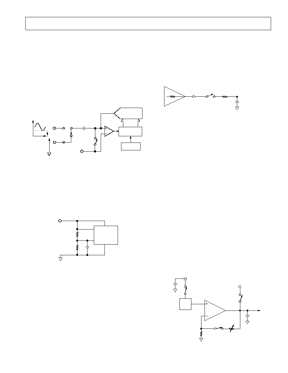
Figure 4 shows a typical connection diagram for the AD7811/
AD7812. The AGND and DGND are connected together at
the device for good noise suppression. The serial interface is
implemented using three wires with RFS/TFS connected to
CONVST see Serial Interface section for more details. V
REF
is
connected to a well decoupled V
DD
pin to provide an analog
input range of 0 V to V
DD
. If the AD7811 or AD7812 is not
sharing a serial bus with another AD7811 or AD7812 then A0
(package address pin) should be hardwired low. The default
power up value of the package address bit in the control register
is 0. For applications where power consumption is of concern,
the automatic power down at the end of a conversion should be
used to improve power performance. See Power-Down Options
section of the data sheet.
SUPPLY
2.7V TO 5.5V
10 F
µC/µP
THREE-WIRE
SERIAL
INTERFACE
10nF
V
REF
DIN
SCLK
CONVST
V
DD
C
REF
V
IN1
AGND
TFS
RFS
DOUT
A0
DGND
0.1 F
V
IN2
V
IN4(8)
AD7811/
AD7812
0V TO
V
REF
INPUT
Figure 4. Typical Connection Diagram
Analog Input
Figure 5 shows an equivalent circuit of the analog input struc-
ture of the AD7811 and AD7812. The two diodes D1 and D2
provide ESD protection for the analog inputs. Care must be
taken to ensure that the analog input signal never exceeds the
supply rails by more than 200 mV. This will cause these diodes
to become forward biased and start conducting current into
the substrate. 20 mA is the maximum current these diodes can
conduct without causing irreversible damage to the part. How-
ever, it is worth noting that a small amount of current (1 mA)
being conducted into the substrate due to an overvoltage on an
unselected channel can cause inaccurate conversions on a
selected channel. The capacitor C2 in Figure 5 is typically about
4 pF and can primarily be attributed to pin capacitance. The
resistor R1 is a lumped component made up of the on resistance
of a multiplexer and a switch. This resistor is typically about
125
. The capacitor C1 is the ADC sampling capacitor and
has a capacitance of 3.5 pF.
CONVERSION PHASE ≠ SWITCH OPEN
TRACK PHASE ≠ SWITCH CLOSED
V
IN
D1
D2
V
DD
/3
C1
3.5pF
R1
125
C2
4pF
V
DD
Figure 5. Equivalent Analog Input Circuit
The analog inputs on the AD7811 and AD7812 can be config-
ured as single ended with respect to analog ground (AGND),
as pseudo differential with respect to a common, and also as
pseudo differential pairs--see Control Register section.
AD7811/AD7812
≠11≠
REV. B
An example of the pseudo differential scheme using the AD7811
is shown in Figure 6. The relevant bits in the AD7811 Control
Register are set as follows DIF/
SGL = 1, CH1 = CH2 = 0, i.e.,
V
IN1
pseudo differential with respect to V
IN2
. The signal is
applied to V
IN1
but in the pseudo differential scheme the sam-
pling capacitor is connected to V
IN2
during conversion and not
AGND as described in the Converter Operation section. This
input scheme can be used to remove offsets that exist in a sys-
tem. For example, if a system had an offset of 0.5 V the offset
could be applied to V
IN2
and the signal applied to V
IN1
. This has
the effect of offsetting the input span by 0.5 V. It is only pos-
sible to offset the input span when the reference voltage is less
than V
DD
≠OFFSET.
V
IN1
V
DD
/3
COMPARATOR
CONTROL
LOGIC
CLOCK
OSC
CONVERSION
PHASE
V
OFFSET
SAMPLING
CAPACITOR
V
IN+
V
IN≠
V
IN2
V
IN1
CHARGE
REDISTRIBUTION
DAC
V
OFFSET
Figure 6. Pseudo Differential Input Scheme
When using the pseudo differential input scheme the signal on
V
IN2
must not vary by more than a 1/2 LSB during the conver-
sion process. If the signal on V
IN2
varies during conversion, the
conversion result will be incorrect. In single-ended mode the
sampling capacitor is always connected to AGND during con-
version. Figure 7 shows the AD7811/AD7812 pseudo differen-
tial input being used to make a unipolar dc current measurement.
A sense resistor is used to convert the current to a voltage and
the voltage is applied to the differential input as shown.
R
L
R
SENSE
AD7811/
AD7812
V
IN+
V
IN≠
V
DD
Figure 7. DC Current Measurement Scheme
DC Acquisition Time
The ADC starts a new acquisition phase at the end of a conver-
sion and ends on the falling edge of the
CONVST signal. At the
end of a conversion a settling time is associated with the sam-
pling circuit. This settling time lasts approximately 100 ns. The
analog signal on V
IN+
is also being acquired during this settling
time. Therefore, the minimum acquisition time needed is
approximately 100 ns.
Figure 8 shows the equivalent charging circuit for the sampling
capacitor when the ADC is in its acquisition phase. R2 repre-
sents the source impedance of a buffer amplifier or resistive
network; R1 is an internal multiplexer resistance, and C1 is the
sampling capacitor. During the acquisition phase the sampling
capacitor must be charged to within a 1/2 LSB of its final value.
The time it takes to charge the sampling capacitor (T
CHARGE
) is
given by the following formula:
T
CHARGE
= 7.6
◊ (R2 + 125 ) ◊ 3.5 pF
C1
3.5pF
V
IN+
R1
125
R2
SAMPLING
CAPACITOR
Figure 8. Equivalent Sampling Circuit
For small values of source impedance, the settling time associ-
ated with the sampling circuit (100 ns) is, in effect, the acquisi-
tion time of the ADC. For example, with a source impedance
(R2) of 10
the charge time for the sampling capacitor is
approximately 4 ns. The charge time becomes significant for
source impedances of 2 k
and greater.
AC Acquisition Time
In ac applications it is recommended to always buffer analog
input signals. The source impedance of the drive circuitry must
be kept as low as possible to minimize the acquisition time of
the ADC. Large values of source impedance will cause the THD
to degrade at high throughput rates. In addition, better perfor-
mance can generally be achieved by using an External 1 nF
capacitor on V
IN
.
ON-CHIP REFERENCE
The AD7811 and AD7812 have an on-chip 2.5 V reference
circuit. The schematic in Figure 9 shows how the reference
circuit is implemented. A 1.23 V bandgap reference is gained up
to provide a 2.5 V
± 2% reference voltage. The on-chip refer-
ence is not available externally (SW2 is open). An external refer-
ence (1.2 V to V
DD
) can be applied at the V
REF
pin. However in
order to use an external reference the EXTREF bit in the con-
trol register (Bit 0) must first be set to a Logic 1. When EXTREF
is set to a Logic 1 SW2 will close, SW3 will open and the ampli-
fier will power down. This will reduce the current consumption
of the part by about 1 mA. It is possible to use two different
reference voltages by selecting the on-chip reference or external
reference.
7pF
2.5V
EXTERNAL
CAPACITOR
1.23V
V
REF
C
REF
AGND
SW3
SW2
SW1
Figure 9. On-Chip Reference Circuitry

AD7811/AD7812
≠12≠
REV. B
When using automatic power-down between conversions to
improve the power performance of the part (see Power vs.
Throughput) the switch SW1 will open when the part enters its
power-down mode if using the internal on-chip reference. This
provides a high impedance discharge path for the external
capacitor (see Figure 9). A typical value of external capacitance
is 10 nF. When the part is in Mode 2 Full Power-Down, because
the external capacitor holds its charge during power-down, the
internal bandgap reference will power up more quickly after
relatively short periods of full power-down. When operating the
part in Mode 2 Partial Power-Down the external capacitor is not
required as the on-chip reference stays powered up while the
rest of the circuitry powers down.
ADC TRANSFER FUNCTION
The output coding of the AD7811 and AD7812 is straight
binary. The designed code transitions occur at successive inte-
ger LSB values (i.e., 1 LSB, 2 LSBs, etc.). The LSB size is =
V
REF
/1024. The ideal transfer characteristic for the AD7811 and
AD7812 is shown in Figure 10.
000...000
0V
ANALOG INPUT
111...111
000...001
000...010
111...110
111...000
011...111
1LSB
+V
REF
≠1LSB
1LSB = V
REF
/1024
ADC CODE
Figure 10. AD7811 and AD7812 Transfer Characteristic
POWER-DOWN OPTIONS
The AD7811 and AD7812 provide flexible power management
to allow the user to achieve the best power performance for a
given throughput rate.
The power management options are selected by programming
the power-down bits (i.e., PD1 and PD0) in the control register.
Table III below summarizes the options available. When the
power-down bits are programmed for Mode 2 Power Down (full
and partial), a rising edge on the
CONVST pin will power up
the part. This feature is used when powering down between
conversions--see Power vs. Throughput. When the AD7811
and AD7812 are placed in partial power-down the on-chip
reference does not power down. However, the part will power
up more quickly after long periods of power-down when using
partial power-down--see Power-Up Times section.
Table III. AD7811/AD7812 Power-Down Options
PD1
PD0
CONVST*
Description
1
1
x
Full Power-Up
0
0
x
Full Power-Down
0
1
0
Mode 2 Partial Power-Down
(Reference Stays Powered-Up)
0
1
1
No Power-Down
1
0
0
Mode 2 Full Power-Down
1
0
1
No Power-Down
*This refers to the state of the CONVST signal at the end of a conversion.
POWER-ON-RESET
If during normal operation, a power-save is performed by removing
power from the AD7811 and AD7812; the user must be wary
that a proper reset is done when power is applied to the part
again. To ensure proper power-on-reset, we recommend that
both PD bits are set to 0 and then set to 1. This procedure
causes an internal reset to occur.
POWER-UP TIMES
The AD7811 and AD7812 have a 1.5
µs power-up time when
using an external reference or when powering up from partial
power-down. When V
DD
is first connected, the AD7811 and
AD7812 are in a low current mode of operation. In order to
carry out a conversion the AD7811 and AD7812 must first be
powered up by writing to the control register of each ADC to
set the power-down bits (i.e., PD1 = 1, PD0 = 1) for a full
power-up. See the Quick Evaluation Setup section on the fol-
lowing page.
Mode 2 Full Power-Down (PD1 = 1, PD0 = 0)
The power-up time of the AD7811 and AD7812 after power is
first connected, or after a long period of Full Power-Down, is
the time it takes the on-chip 1.23 V reference to power up plus
the time it takes to charge the external capacitor C
REF
--see
Figure 9. The time taken to charge C
REF
to the 10-bit level is
given by the equation (7.6
◊ 2 k ◊ C
REF
). For C
REF
= 10 nF
the power-up time is approximately 152
µs. It takes 30 µs to
power up the on-chip reference so the total power-up time of
either ADC in either of these conditions is 182
µs. However,
when powering down fully between conversions to achieve a
better power performance this power-up time reduces to 1.5
µs
after a relatively short period of power-down as C
REF
holds its
charge (see On-Chip Reference section). The AD7811 and
AD7812 can therefore be used in Mode 2 with throughput
rates of 250 kSPS and under.
Mode 2 Partial Power-Down (PD1 = 0, PD0 = 1)
The power-up time of the AD7811 and AD7812 from a Partial
Power-Down is 1.5
µs maximum. When using a Partial Power-
Down between conversions, there is no requirement to connect
an external capacitor to the C
REF
pin because the reference
remains powered up. This means that the AD7811 and AD7812
will power up in 30
µs after the supplies are first connected as
there is no requirement to charge an external capacitor.
POWER VS. THROUGHPUT
By using the Automatic Power-Down (Mode 2) at the end of a
conversion--see Operating Modes section of the data sheet,
superior power performance can be achieved.
Figure 11 shows how the Automatic Power-Down is implemented
using the
CONVST signal to achieve the optimum power
performance for the AD7811 and AD7812. The AD7811 and
AD7812 are operated in Mode 2 and the control register Bits
PD1 and PD0 are set to 1 and 0 respectively for Full Power-Down,
or 0 and 1 for Partial Power-Down. The duration of the
CONVST
pulse is set to be equal to or less than the power-up time of the
devices--see Operating Modes section. As the throughput rate
is reduced, the device remains in its power-down state longer
and the average power consumption over time drops accordingly.
AD7811/AD7812
≠13≠
REV. B
t
POWER-UP
1.5 s
CONVST
t
CONVERT
2.3 s
100 s @ 10kSPS
POWER-DOWN
t
CYCLE
Figure 11. Automatic Power-Down
For example, if the AD7811 is operated in a continuous sam-
pling mode with a throughput rate of 10 kSPS, PD1 = 1,
PD0 = 0 and using the on chip reference the power consump-
tion is calculated as follows. The power dissipation during nor-
mal operation is 10.5 mW, V
DD
= 3 V. If the power-up time is
1.5
µs and the conversion time is 2.3 µs, the AD7811 can be
said to dissipate 10.5 mW for 3.8
µs (worst-case) during each
conversion cycle. If the throughput rate is 10 kSPS, the cycle
time is 100
µs and the average power dissipated during each
cycle is (3.8/100)
◊ (10.5 mW) = 400 µW.
Figure 12 shows the Power vs. Throughput Rate for automatic
full power-down.
THROUGHPUT ≠ kSPS
10
1
0.01
0
50
10
0.1
20
30
40
5
15
25
35
45
POWER
≠
mV
Figure 12. AD7811/AD7812 Power vs. Throughput
FREQUENCY ≠ kHz
0
≠10
≠100
0
122
17
87
105
≠40
≠70
≠80
≠90
≠20
≠30
≠60
≠50
35
52
70
140
157
174
AD7811/12
2048 POINT FFT
SAMPLING 357.142kHz
f
IN
= 30.168kHz
dBs
Figure 13. AD7811/AD7812 SNR
QUICK EVALUATION SETUP
The schematic shown in Figure 14 shows a suggested configura-
tion of the AD7812 for a first look evaluation of the part. No
external reference circuit is needed as the V
REF
pin can be
connected to V
DD
. The
CONVST signal is connected to TFS
and RFS to enable the serial port. Also by selecting Mode 2
operation (see Operating Modes section) the power performance
of the AD7812 can be evaluated.
10 F
10nF
V
REF
DIN
SCLK
CONVST
V
DD
C
REF
V
IN1
AGND
TFS
RFS
DOUT
A0
DGND
0.1 F
V
IN2
AD7812
0V TO V
DD
INPUT
V
IN7
V
IN8
SUPPLY
V
DD
Figure 14. Evaluation Quick Setup
The setup uses a full duplex, 16-bit, serial interface protocol,
e.g., SPI. It is possible to use 8-bit transfers by carrying out two
consecutive read/write operations. The MSB of data is trans-
ferred first.
1. When power is first connected to the device it is in a powered
down mode of operation and is consuming only 1
µA. The
AD7812 must first be configured by carrying out a serial
write operation.
2. The
CONVST signal is first pulsed to enable the serial port
(rising and falling edge on RFS and TFS respectively--see
Serial Interface section).
3. Next, a 16-bit serial read/write operation is carried out. By
writing 6040 Hex to the AD7812 the part is powered up, set
up to use external reference (i.e., V
DD
) and the analog input
V
IN1
is selected. The data read from the part during this read/
write operation is invalid.
4. It is necessary to wait approximately 1.5
µs before pulsing
CONVST again and initiating a conversion. The 1.5
µs is to
allow the AD7812 to power up correctly--see Power-Up
Times section.
5. Approximately 2.3
µs after the falling edge of CONVST, i.e.,
after the end of the conversion, a serial read/write can take
place. This time 4040 Hex is written to the AD7812 and the
data read from the part is the result of the conversion. The
output code is in a straight binary format and will be left
justified in the 16-bit serial register (MSB clocked out first).
6. By idling the
CONVST signal high or low it is possible to
operate the AD7812 in Mode 1 and Mode 2 respectively.

AD7811/AD7812
≠14≠
REV. B
DIN
DOUT
CONVST
V
DD
6040 HEX
NOT VALID
4040 HEX
VALID DATA
VALID DATA
4040 HEX
t
POWER-UP
1.5 s
t
CONVERT
2.3 s
t
CONVERT
2.3 s
Figure 15. Read/Write Sequence for AD7812
OPERATING MODES
The mode of operation of the AD7811 and AD7812 is selected
when the (logic) state of the
CONVST is checked at the end of
a conversion. If the
CONVST signal is logic high at the end
of a conversion, the part does not power down and is operat-
ing in Mode 1. If, however, the
CONVST signal is brought
logic low before the end of a conversion, the AD7811 and AD7812
will power down at the end of the conversion. This is Mode 2
operation.
Mode 1 Operation (High Speed Sampling)
When the AD7811 and AD7812 are operated in Mode 1 they
are not powered down between conversions. This mode of opera-
tion allows high throughput rates to be achieved. The timing
diagram in Figure 16 shows how this optimum throughput rate
is achieved by bringing the
CONVST signal high before the end
of the conversion.
The sampling circuitry leaves its tracking mode and goes into
hold on the falling edge of
CONVST. A conversion is also initi-
ated at this time. The conversion takes 2.3
µs to complete. At
this point, the result of the current conversion is latched into the
serial shift register and the state of the
CONVST signal checked.
The
CONVST signal should be logic high at the end of the
conversion to prevent the part from powering down. The serial
port on the AD7811 and AD7812 is enabled on the rising edge
of the first SCLK after the rising edge of the RFS signal--see
Serial Interface section. As explained earlier, this rising edge
should occur before the end of the conversion process if the part
is not to be powered down. A serial read can take place at any
stage after the rising edge of
CONVST. If a serial read is initi-
ated before the end of the current conversion process (i.e., at
time "A"), the result of the previous conversion is shifted out on
the DOUT pin. It is possible to allow the serial read to extend
beyond the end of a conversion. In this case the new data will
not be latched into the output shift register until the read
has finished. The dynamic performance of the AD7811 and
AD7812 typically degrades by up to 3 dBs while reading during
a conversion. If the user waits until the end of the conversion
process, i.e., 2.3
µs after the falling edge of CONVST (Point
"B") before initiating a read, the current conversion result is
shifted out. The serial read must finish at least 100 ns prior to
the next falling edge of
CONVST to allow the part to accurately
acquire the input signal.
Mode 2 Operation (Automatic Power-Down)
When used in this mode of operation the part automatically
powers down at the end of a conversion. This is achieved by
leaving the
CONVST signal low until the end of the conversion.
Because it takes approximately 1.5
µs for the part to power-up
after it has been powered down, this mode of operation is intended
to be used in applications where slower throughput rates are
required, i.e., in the order of 250 kSPS and improved power
performance is required--see Power vs. Throughput section.
There are two power-down modes the AD7811/AD7812 can
CURRENT CONVERSION
RESULT
A
B
t
12
CONVST
DOUT
SCLK
t
1
t
2
Figure 16. Mode 1 Operation Timing Diagram

AD7811/AD7812
≠15≠
REV. B
enter during automatic power-down. These modes are discussed
in the Power-Up Times section of this data sheet. The timing
diagram in Figure 17 shows how to operate the part in Mode 2.
If the AD7811/AD7812 is powered down, the rising edge of the
CONVST pulse causes the part to power-up. Once the part
has powered up (~1.5
µs after the rising edge of CONVST)
the
CONVST signal is brought low and a conversion is initiated
on this falling edge of the
CONVST signal. The conversion
takes 2.3
µs and after this time the conversion result is latched
into the serial shift register and the part powers down. There-
fore, when the part is operated in Mode 2 the effective conver-
sion time is equal to the power-up time (1.5
µs) and the SAR
conversion time (2.3
µs).
NOTE: Although the AD7811 and AD7812 take 1.5
µs to
power up after the rising edge of
CONVST, it is not necessary
to leave
CONVST high for 1.5
µs after the rising edge before
bringing it low to initiate a conversion. If the
CONVST signal
goes low before 1.5
µs in time has elapsed, then the power-up
time is timed out internally and a conversion is then initiated.
Hence the AD7811 and AD7812 are guaranteed to have always
powered-up before a conversion is initiated, even if the
CONVST
pulsewidth is <1.5
µs. If the CONVST pulsewidth is > 1.5 µs,
then a conversion is initiated on the falling edge.
As in the case of Mode 1 operation, the rising edge of the first
SCLK after the rising edge of RFS enables the serial port of the
AD7811 and AD7812 (see Serial Interface section). If a serial
read is initiated soon after this rising edge (Point "A"), i.e.,
before the end of the conversion, the result of the previous con-
version is shifted out on pin DOUT. In order to read the result
of the current conversion, the user must wait at least 2.3
µs after
power-up or at least 2.3
µs after the falling edge of CONVST,
(Point "B"), whichever occurs latest before initiating a serial
read. The serial port of the AD7811 and AD7812 is still func-
tional even though the devices have been powered down.
Because it is possible to do a serial read from the part while it is
powered down, the AD7811 and AD7812 are powered up only
to do the conversion and are immediately powered down at the
end of a conversion. This significantly improves the power
consumption of the part at slower throughput rates--see Power
vs. Throughput section.
SERIAL INTERFACE
The serial interface of the AD7811 and AD7812 consists of five
wires, a serial clock input, SCLK, receive data to clock syn-
chronization input RFS, transmit data to clock synchronization
input TFS, a serial data output, DOUT, and a serial data
input, DIN, (see Figure 18). The serial interface is designed to
allow easy interfacing to most microcontrollers and DSPs,
e.g., PIC16C, PIC17C, QSPI, SPI, DSP56000, TMS320
and ADSP-21xx, without the need for any gluing logic. When
interfacing to the 8051, the SCLK must be inverted. The
Microprocessor/Microcontroller Interface section explains
how to interface to some popular DSPs and microcontrollers.
Figure 18 shows the timing diagram for a serial read and write
to the AD7811 and AD7812. The serial interface works with
both a continuous and a noncontinuous serial clock. The rising
edge of RFS and falling edge of TFS resets a counter that
counts the number of serial clocks to ensure the correct number
of bits are shifted in and out of the serial shift registers. Once
the correct number of bits have been shifted in and out, the
SCLK is ignored. In order for another serial transfer to take
place the counter must be reset by the active edges of TFS and
CURRENT CONVERSION
RESULT
A
B
t
POWER-UP
CONVST
DOUT
SCLK
1.5 s
t
1
t
2
Figure 17. Mode 2 Operation Timing Diagram
A
B
DIN
DB9
DB8
DB9
DB7
DB8
DB7
DB6
DB5
DB4
DB3
DB0
SCLK
RFS
DOUT
t
3
t
7
t
4
t
10
DB1
DB2
1
13
12
11
10
9
8
7
6
5
4
3
2
TFS
t
8
t
9
t
5
t
6
DB6
DB5
DB4
DB3
DB2
DB1
DB0
Figure 18. Serial Interface Timing Diagram
AD7811/AD7812
≠16≠
REV. B
RFS. The first rising SCLK edge after the rising edge of the
RFS signal causes DOUT to leave its high impedance state and
data is clocked out onto the DOUT line and also on subsequent
SCLK rising edges. The DOUT pin goes back into a high
impedance state on the 11th SCLK rising edge--Point "A" on
Figure 18. A minimum of 11 SCLKs are therefore needed to
carry out a serial read. Data on the DIN line is latched in on
the first SCLK falling edge after the falling edge of the TFS
signal and on subsequent SCLK falling edges. The control
register is updated on the 13th SCLK rising edge--point "B" on
Figure 18. A minimum of 13 SCLK pulses are therefore needed
to complete a serial write operation. In multipackage applications
the RFS and TFS signals can be used as chip select signals. The
serial interface will not shift data in or out until it receives the
active edge of the RFS or TFS signal.
Simplifying the Serial Interface
The five-wire interface is designed to support many different
serial interface standards. However, it is possible to reduce the
number of lines required to just three. By simply connecting the
TFS and RFS pins to the
CONVST signal (see Figure 4), the
CONVST signal can be used to enable the serial port for read-
ing and writing. This is only possible where a noncontinuous
serial clock is being used.
MICROPROCESSOR INTERFACING
The serial interface on the AD7811 and AD7812 allows the
parts to be directly connected to a range of many different
microprocessors. This section explains how to interface the
AD7811 and AD7812 with some of the more common micro-
controller and DSP serial interface protocols.
AD7811/AD7812 to PIC16C6x/7x
The PIC16C6x Synchronous Serial Port (SSP) is configured as
an SPI Master with the Clock Polarity bit = 0. This is done
by writing to the Synchronous Serial Port Control Register
(SSPCON). See user PIC16/17 Microcontroller User Manual.
Figure 19 shows the hardware connections needed to interface
to the PIC16/17. In this example I/O port RA1 is being used to
pulse
CONVST and enable the serial port of the AD7811/
AD7812. This microcontroller transfers only eight bits of data
during each serial transfer operation; therefore, two consecutive
read/write operations are needed.
CONVST
AD7811/AD7812*
DOUT
DIN
SCLK
RFS
TFS
PIC16C6x/7x*
SCK/RC3
SDO/RC5
SDI/ RC4
RA1
*ADDITIONAL PINS OMITTED FOR CLARITY
Figure 19. Interfacing to the PIC16/17
AD7811/AD7812 to MC68HC11
The Serial Peripheral Interface (SPI) on the MC68HC11 is
configured for Master Mode (MSTR = 0), Clock Polarity Bit
(CPOL) = 0 and the Clock Phase Bit (CPHA) = 1. The SPI is
configured by writing to the SPI Control Register (SPCR)--see
68HC11 user manual. A connection diagram is shown in
Figure 20.
CONVST
AD7811/AD7812*
DOUT
DIN
SCLK
RFS
TFS
MC68HC11*
SCLK/PD4
MISO/PD2
MOSI/PD3
PA0
*ADDITIONAL PINS OMITTED FOR CLARITY
Figure 20. Interfacing to the MC68HC11
AD7811/AD7812 to 8051
The AD7811/AD7812 requires a clock synchronized to the
serial data. The 8051 serial interface must therefore be operated
in Mode 0. In this mode serial data enters and exits through
RxD and a shift clock is output on TxD (half duplex). Figure 21
shows how the 8051 is connected to the AD7811/AD7812.
However, because the AD7811/AD7812 shifts data out on the
rising edge of the shift clock and latches data in on the falling
edge, the shift clock must be inverted.
AD7811/AD7812*
DOUT
DIN
SCLK
TFS
8051*
TxD
RxD
P1.1
*ADDITIONAL PINS OMITTED FOR CLARITY
RFS
Figure 21. Interfacing to the 8051 Serial Port

AD7811/AD7812
≠17≠
REV. B
It is possible to implement a serial interface using the data ports
on the 8051. This would also allow a full duplex serial transfer
to be implemented. The technique involves "bit banging" an
I/O port (e.g., P1.0) to generate a serial clock and using two
other I/O ports (e.g., P1.1 and P1.2) to shift data in and out--
see Figure 22.
AD7811/AD7812*
DOUT
DIN
SCLK
RFS
TFS
8051*
P1.0
P1.1
P1.2
P1.3
*ADDITIONAL PINS OMITTED FOR CLARITY
Figure 22. Interfacing to the 8051 Using I/O Ports
AD7811/AD7812 to TMS320C5x
The serial interface on the TMS320C5x uses a continuous
serial clock and frame synchronization signals to synchronize
the data transfer operations with peripheral devices like the
AD7811. Frame synchronization inputs have been supplied on
the AD7811/AD7812 to allow easy interfacing with no extra
gluing logic. The serial port of the TMS320C5x is set up to
operate in Burst Mode with internal CLKX (Tx serial clock)
and FSX (Tx frame sync). The Serial Port Control register
(SPC) must have the following setup: F0 = 0, FSM = 1,
MCM = 1 and TXM = 1. The connection diagram is shown
in Figure 23.
AD7811/AD7812*
DOUT
SCLK
RFS
TFS
TMS320C5x*
CLKX
CLKR
FSX
*ADDITIONAL PINS OMITTED FOR CLARITY
FSR
DR
DIN
DT
Figure 23. Interfacing to the TMS320C5x
AD7811/AD7812 to ADSP-21xx
The ADSP-21xx family of DSPs are easily interfaced to the
AD7811/AD7812 without the need for extra gluing logic. The
SPORT is operated in normal framing mode. The SPORT
control register should be set up as follows:
TFSW
= RFSW = 0, Normal Framing
INVRFS = INVTFS = 0, Active High Frame Signal
DTYPE = 00, Right Justify Data
SLEN
= 1001, 10-Bit Data Words
ISCLK
= 1, Internal Serial Clock
TFSR
= RFSR = 1, Frame Every Word
IRFS
= 0, External Framing Signal
ITFS
= 1, Internal Framing Signal
The 10-bit data words will be right justified in the 16-bit serial
data registers when using this configuration. Figure 24 shows
the connection diagram.
AD7811/AD7812*
DOUT
DIN
SCLK
RFS
TFS
ADSP-21xx*
SCLK
DR
DT
RFS
*ADDITIONAL PINS OMITTED FOR CLARITY
TFS
Figure 24. Interfacing to the ADSP-21xx
AD7811/AD7812 to DSP56xxx
The connection diagram in Figure 25 shows how the AD7811
and AD7812 can be connected to the SSI (Synchronous Serial
Interface) of the DSP56xxx family of DSPs from Motorola. The
SSI is operated in Synchronous Mode (SYN bit in CRB =1)
with internally generated 1-bit clock period frame sync for both
Tx and Rx (FSL1 and FSL0 bits in CRB = 1 and 0 respectively).
AD7811/AD7812*
DOUT
SCLK
DSP56xxx*
SCK
SRD
*ADDITIONAL PINS OMITTED FOR CLARITY
DIN
STD
SC2
RFS
TFS
Figure 25. Interfacing to the DSP56xxx
AD7811/AD7812
≠18≠
REV. B
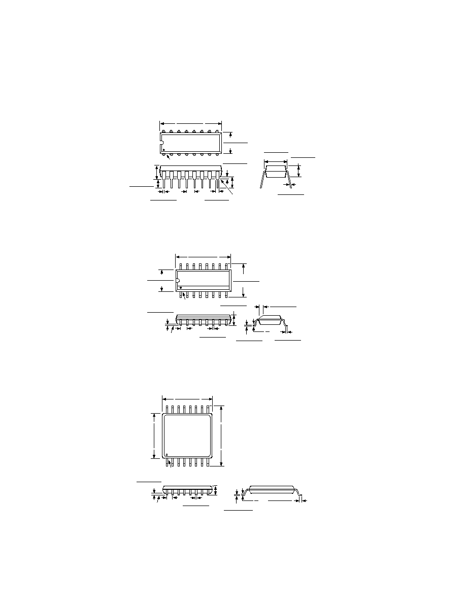
OUTLINE DIMENSIONS
Dimensions shown in inches and (mm).
16-Lead Plastic DIP
(N-16)
16
1
8
9
0.840 (21.33)
0.745 (18.93)
0.280 (7.11)
0.240 (6.10)
PIN 1
SEATING
PLANE
0.022 (0.558)
0.014 (0.356)
0.060 (1.52)
0.015 (0.38)
0.210 (5.33)
MAX
0.130
(3.30)
MIN
0.070 (1.77)
0.045 (1.15)
0.100
(2.54)
BSC
0.160 (4.06)
0.115 (2.93)
0.325 (8.25)
0.300 (7.62)
0.015 (0.381)
0.008 (0.204)
0.195 (4.95)
0.115 (2.93)
16-Lead Small Outline Package (SOIC)
(R-16A)
16
9
8
1
0.3937 (10.00)
0.3859 (9.80)
0.2550 (6.20)
0.2284 (5.80)
0.1574 (4.00)
0.1497 (5.80)
PIN 1
SEATING
PLANE
0.0098 (0.25)
0.0040 (0.10)
0.0192 (0.49)
0.0138 (0.35)
0.0688 (1.75)
0.0532 (1.35)
0.0500
(1.27)
BSC
0.0099 (0.25)
0.0075 (0.19)
0.0500 (1.27)
0.0160 (0.41)
8
∞
0
∞
0.0196 (0.50)
0.0099 (0.25)
x 45
∞
16-Lead Thin Shrink Outline Package (TSSOP)
(RU-16)
16
9
8
1
0.201 (5.10)
0.193 (4.90)
0.256 (6.50)
0.246 (6.25)
0.177 (4.50)
0.169 (4.30)
PIN 1
SEATING
PLANE
0.006 (0.15)
0.002 (0.05)
0.0118 (0.30)
0.0075 (0.19)
0.0256
(0.65)
BSC
0.0433
(1.10)
MAX
0.0079 (0.20)
0.0035 (0.090)
0.028 (0.70)
0.020 (0.50)
8
∞
0
∞
AD7811/AD7812
≠19≠
REV. B
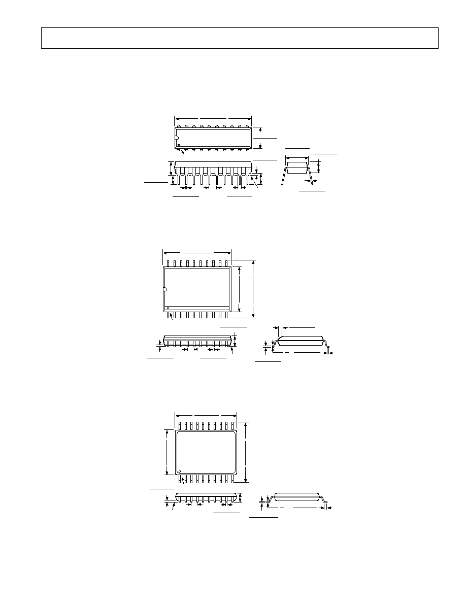
OUTLINE DIMENSIONS
Dimensions shown in inches and (mm).
20-Lead Plastic DIP
(N-20)
20
1
10
11
1.060 (26.90)
0.925 (23.50)
0.280 (7.11)
0.240 (6.10)
PIN 1
SEATING
PLANE
0.022 (0.558)
0.014 (0.356)
0.210 (5.33)
MAX
0.130
(3.30)
MIN
0.070 (1.77)
0.045 (1.15)
0.100
(2.54)
BSC
0.160 (4.06)
0.115 (2.93)
0.060 (1.52)
0.015 (0.38)
0.325 (8.25)
0.300 (7.62)
0.015 (0.381)
0.008 (0.204)
0.195 (4.95)
0.115 (2.93)
20-Lead Small Outline Package (SOIC)
(R-20A)
SEATING
PLANE
0.0118 (0.30)
0.0040 (0.10)
0.0192 (0.49)
0.0138 (0.35)
0.1043 (2.65)
0.0926 (2.35)
0.0500
(1.27)
BSC
0.0125 (0.32)
0.0091 (0.23)
0.0500 (1.27)
0.0157 (0.40)
8
∞
0
∞
0.0291 (0.74)
0.0098 (0.25)
x 45
∞
20
11
10
1
0.5118 (13.00)
0.4961 (12.60)
0.4193 (10.65)
0.3937 (10.00)
0.2992 (7.60)
0.2914 (7.40)
PIN 1
20-Lead Thin Shrink Outline Package (TSSOP)
(RU-20)
20
11
10
1
0.260 (6.60)
0.252 (6.40)
0.256 (6.50)
0.246 (6.25)
0.177 (4.50)
0.169 (4.30)
PIN 1
SEATING
PLANE
0.006 (0.15)
0.002 (0.05)
0.0118 (0.30)
0.0075 (0.19)
0.0256 (0.65)
BSC
0.0433
(1.10)
MAX
0.0079 (0.20)
0.0035 (0.090)
0.028 (0.70)
0.020 (0.50)
8
∞
0
∞
C01312a≠0≠10/00 (rev. B)
PRINTED IN U.S.A.