
REV. A
Information furnished by Analog Devices is believed to be accurate and
reliable. However, no responsibility is assumed by Analog Devices for its
use, nor for any infringements of patents or other rights of third parties that
may result from its use. No license is granted by implication or otherwise
under any patent or patent rights of Analog Devices.
AD10265
FEATURES
Dual, 65 MSPS Minimum Sample Rate
Channel-Channel Matching, 0.1% Gain Error
Channel-Channel Isolation, >80 dB
AC-Coupled Signal Conditioning Included
Selectable Bipolar Input Voltage Range
( 0.5 V, 1.0 V, 2.0 V)
Gain Flatness up to Nyquist: < 0.5 dB
80 dB Spurious-Free Dynamic Range
Two's Complement Output Format
3.3 V or 5 V CMOS-Compatible Output Levels
1.05 W Per Channel
Industrial and Military Grade
APPLICATIONS
Phased Array Receivers
Communications Receivers
FLIR Processing
Secure Communications
GPS Anti-Jamming Receivers
Multichannel, Multimode Receivers
FUNCTIONAL BLOCK DIAGRAM
D11B (MSB)
D10B
D9B
D8B
D7B
D0B
(LSB)
D1B
D2B
D3B
D4B
D5B
D6B
D9A
D10A
D11A
(MSB)
(LSB) D0A
D1A
D2A
D3A
D4A
D5A
D6A
D7A
D8A
ENCODEA
5
7
12
A
IN
B3
ENCODEB
ENCODEB
TIMING
ENCODEA
9
AD9631
AD9632
AIN
AIN
A
IN
A2
A
IN
A1
A
IN
A3
12
AD6640
OUTPUT BUFFERING
AD10265
A
IN
B2
A
IN
B1
OUTPUT BUFFERING
TIMING
AD9631
AD9632
AIN
AIN
AD6640
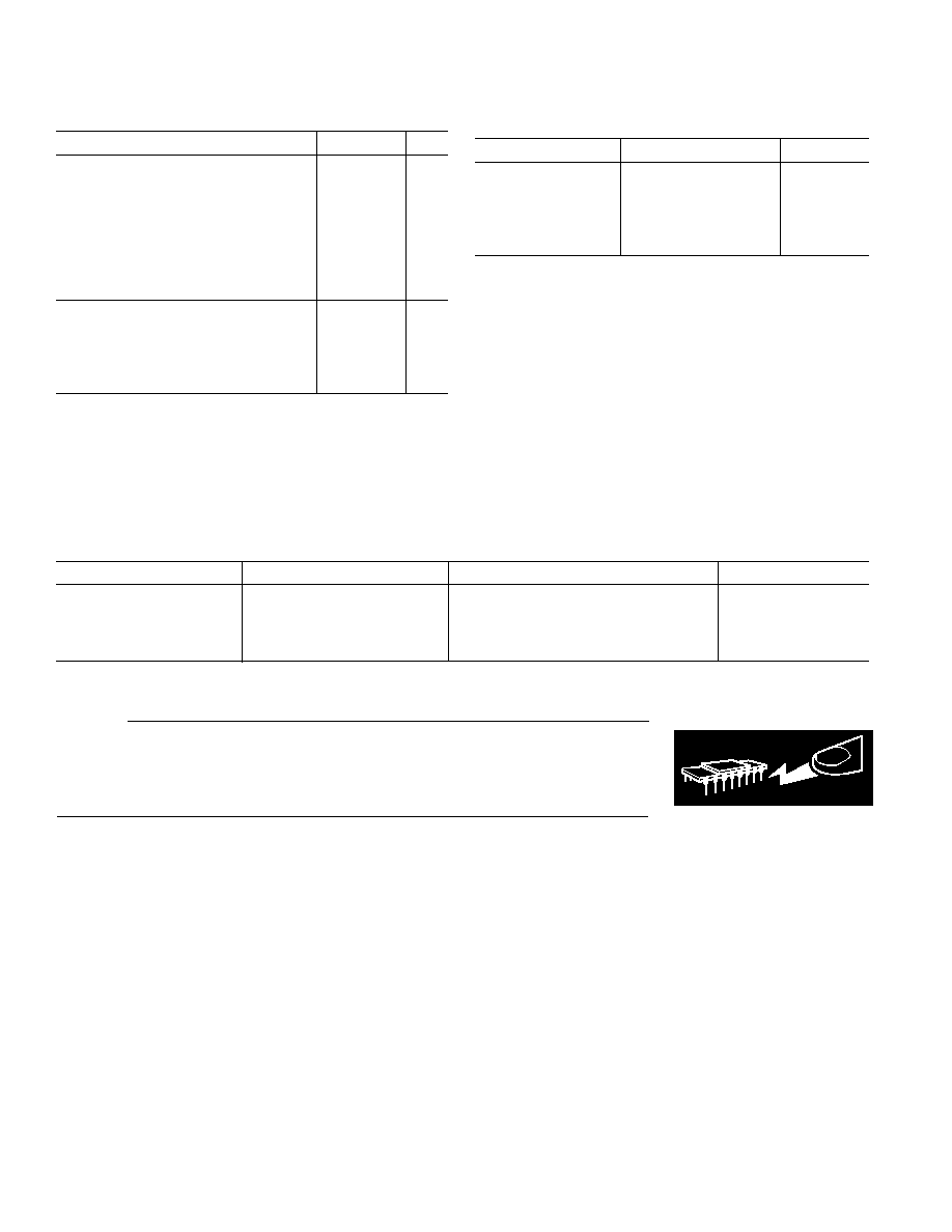
Dual Channel, 12-Bit, 65 MSPS A/D Converter
with Analog Input Signal Conditioning
a
PRODUCT DESCRIPTION
The AD10265 is a full channel ADC solution with on-module
signal conditioning for improved dynamic performance and
fully matched channel-to-channel performance. The module
includes two wide dynamic range AD6640 ADCs. Each AD6640
has an AD9631/AD9632 ac-coupled amplifier front end. The
AD6640s have on-chip track-and-hold circuitry, and utilize an
innovative multipass architecture, to achieve 12-bit, 65 MSPS
performance. The AD10265 uses innovative high-density
circuit design and laser-trimmed thin-film resistor networks to
achieve exceptional matching and performance while still main-
taining excellent isolation, and providing for significant board
area savings.
The AD10265 operates with
� 5.0 V for the analog signal
conditioning with a separate +3.3 V supply for the analog-to-
digital conversion. Each channel is completely independent
allowing operation with independent Encode and Analog
inputs. The AD10265 also offers the user a choice of Analog
Input Signal ranges to further minimize additional external
signal conditioning, while still remaining general-purpose.
The AD10265 is packaged in a 68-lead ceramic gull wing pack-
age, footprint compatible with the earlier generation AD10242
(12-bit, 40 MSPS). Manufacturing is done on Analog Devices'
MIL-38534 Qualified Manufacturers Line (QML) and com-
ponents are available up to Class-T (�25
�C to +125�C). The
AD6640 internal components are manufactured on Analog
Devices' high-speed complementary bipolar process (XFCB).
PRODUCT HIGHLIGHTS
1. Guaranteed sample rate of 65 MSPS.
2. Input amplitude options, user configurable.
3. Input signal conditioning included; both channels matched
for gain.
4. Fully tested/characterized performance for full channel.
5. Footprint compatible family; 68-lead LCCC.
One Technology Way, P.O. Box 9106, Norwood, MA 02062-9106, U.S.A.
Tel: 781/329-4700
www.analog.com
Fax: 781/326-8703
� Analog Devices, Inc., 2001

REV. A
�2�
AD10265�SPECIFICATIONS
Electrical Characteristics
(AV
CC
= +5 V; AV
EE
= �5.0 V; DV
CC
= +3.3 V; applies to each ADC unless otherwise noted.)
Test
Mil
AD10265AZ
Parameter
Temp
Level
Subgroup
Min
Typ
Max
Unit
RESOLUTION
12
Bits
ACCURACY
No Missing Codes
Full
IV
12
Guaranteed
Offset Error
Full
IV
2, 3
�10
+3.5
+10
mV
Gain Error
1
25
�C
I
1
�1.5
�0.5
+1.5
% FS
Full
VI
2, 3
�2.5
�0.8
+2.5
% FS
Gain Error Channel Match
Full
V
�0.2
%
Pass Band Ripple to Nyquist
Full
IV
12
0.2
0.5
dB
ANALOG INPUT (A
IN
)
Input Voltage Range
A
IN
1
Full
V
�0.5
V
A
IN
2
Full
V
�1.0
V
A
IN
3
Full
V
�2
V
Input Resistance
A
IN
1
Full
IV
12
99
100
101
A
IN
2
Full
IV
12
198
200
202
A
IN
3
Full
IV
12
396
400
404
Input Capacitance
2
25
�C
IV
12
0
4.0
7.0
pF
Analog Input Bandwidth High
3
25
�C
V
160
MHz
Analog Input Bandwidth Low
3
25
�C
V
50
kHz
ENCODE INPUT
4, 5
Logic Compatibility
IV
TTL/CMOS
Logic "1" Voltage
Full
IV
2.0
5.0
V
Logic "0" Voltage
Full
IV
0
0.8
V
Logic "1" Current (V
INH
= 5 V)
Full
IV
500
650
800
�A
Logic "0" Current (V
INL
= 0 V)
Full
IV
�400
�320
�200
�A
Input Capacitance
25
�C
IV
12
4.5
7.0
pF
SWITCHING PERFORMANCE
Maximum Conversion Rate
6
Full
VI
4, 5, 6
65
MSPS
Minimum Conversion Rate
6
Full
IV
12
6.5
MSPS
Aperture Delay (t
A
)
25
�C
V
400
ps
Aperture Delay Matching
25
�C
V
�2.0
ns
Aperture Uncertainty (Jitter)
25
�C
V
0.3
ps rms
ENCODE Pulsewidth High
25
�C
IV
12
6.5
ns
ENCODE Pulsewidth Low
25
�C
IV
12
6.5
ns
Output Delay (t
OD
)
Full
IV
12
7.0
9.0
12.5
ns
SNR
7
Analog Input @ 1.24 MHz
25
�C
I
4
62
66
dB
Full
II
5, 6
60.5
66
dB
@ 17 MHz
25
�C
I
4
61
65
dB
Full
II
5, 6
60
65
dB
@ 32 MHz
25
�C
I
4
61
63
dB
Full
II
5, 6
59.5
62
dB
SINAD
8
Analog Input @ 1.24 MHz
25
�C
I
4
61
65
dB
Full
II
5, 6
60
64
dB
@ 17 MHz
25
�C
I
4
61
64
dB
Full
II
5, 6
59.5
63
dB
@ 32 MHz
25
�C
I
4
61
62
dB
Full
II
5, 6
59
62
dB

Test
Mil
AD10265AZ
Parameter
Temp
Level
Subgroup
Min
Typ
Max
Unit
SPURIOUS-FREE DYNAMIC RANGE
9
Analog Input @ 1.24 MHz
25
�C
I
4
75
80
dBFS
Full
II
5, 6
74
80
dBFS
@ 17 MHz
25
�C
I
4
71
80
dBFS
Full
II
5, 6
70
79
dBFS
@ 32 MHz
25
�C
V
79
dBFS
Full
V
79
dBFS
TWO-TONE IMD REJECTION
10
f1, f2 @ �7 dBFS
Full
V
4, 5, 6
66
77
dBc
CHANNEL-TO-CHANNEL ISOLATION
11
25
�C
IV
12
80
dB
LINEARITY
Differential Nonlinearity
(Encode = 20 MHz)
25
�C
IV
12
�1.0
�0.5
+1.5
LSB
Integral Nonlinearity
(Encode = 20 MHz)
Full
V
�1.25
LSB
DIGITAL OUTPUTS
Logic Compatibility
CMOS
Logic "1" Voltage
Full
I
1, 2, 3
2.8
DV
CC
� 0.2
V
Logic "0" Voltage
Full
I
1, 2, 3
0.2
0.5
V
Output Coding
Two's Complement
POWER SUPPLY
AV
CC
Supply Voltage
Full
V
+5.0
V
I (AV
CC
) Current
Full
V
336
mA
AV
EE
Supply Voltage
Full
V
�5.0
V
I (AV
EE
) Current
Full
V
66
mA
DV
CC
Supply Voltage
Full
V
+3.3
V
I (DV
CC
) Current
Full
V
20
mA
I
CC
(Total) Supply Current
Full
I
1, 2, 3
422
520
mA
Power Dissipation (Total)
Full
I
1, 2, 3
2.1
2.4
W
Power Supply Rejection Ratio (PSRR)
Full
IV
12
0.01
0.02
% FSR/% V
S
NOTES
1
Gain tests are performed on A
IN
1 over specified input voltage range.
2
Input capacitance specifications show only ceramic package capacitance.
3
Full power bandwidth is the frequency at which the spectral power of the fundamental frequency (as determined by FFT analysis) is reduced by 3 dB.
4
ENCODE driven by single-ended source;
ENCODE bypassed to ground through 0.01
�F capacitor.
5
ENCODE may also be driven differentially in conjunction with
ENCODE; see "Encoding the AD10265" for details.
6
Minimum and maximum conversion rates allow for variation in Encode Duty Cycle of 50%
� 5%.
7
Analog Input signal power at �1 dBFS; signal-to-noise ratio (SNR) is the ratio of signal level to total noise (first 5 harmonics removed). Encode = 65 MSPS.
8
Analog Input signal power at �1 dBFS; signal-to-noise and distortion (SINAD) is the ratio of signal level to total noise + harmonics. Encode = 65 MSPS.
9
Analog Input signal equal �1 dBFS; SFDR is ratio of converter full scale to worst spur.
10
Both input tones at �7 dBFS; two-tone intermodulation distortio n (IMD) rejection is the ratio of either tone to the worst third order intermod product. f1 = 17.0 MHz
� 100 kHz, f2 = 18.0 MHz � 100 kHz.
11
Channel-to-channel isolation tested with A channel/50 ohm terminated <A
IN
2 grounded, and a full-scale signal applied to B channel (A
IN
1).
All specifications guaranteed within 100 ms of initial power-up, regardless of sequencing.
Specifications subject to change without notice.
AD10265
�3�
REV. A
AD10265
�4�
REV. A
ABSOLUTE MAXIMUM RATINGS
1
Parameter
Min
Max
Unit
ELECTRICAL
V
CC
Voltage
0
+7
V
V
EE
Voltage
�7
0
V
Analog Input Voltage
V
EE
V
CC
V
Analog Input Current
�10
+10
mA
Digital Input Voltage (ENCODE)
0
AV
CC
V
ENCODE,
ENCODE Differential Voltage
4
V
Digital Output Current
�10
+10
mA
ENVIRONMENTAL
2
Operating Temperature (Case)
�55
+125
�C
Maximum Junction Temperature
175
�C
Lead Temperature (Soldering, 10 sec)
300
�C
Storage Temperature Range (Ambient)
�65
+150
�C
NOTES
1
Absolute maximum ratings are limiting values to be applied individually, and
beyond which the serviceability of the circuit may be impaired. Functional
operability is not necessarily implied. Exposure to absolute maximum rating
conditions for an extended period of time may affect device reliability.
2
Typical thermal impedances for "Z" package:
JC
= 11
�C/W;
JA
= 30
�C/W.
Table I. Output Coding
MSB LSB
Base 10
Input
0111111111111
2047
+FS
0000000000001
+1
0000000000000
0
0.0 V
1111111111111
�1
1000000000000
2048
�FS
EXPLANATION OF TEST LEVELS
Test Level
I.
100% production tested.
II.
100% production tested at 25
�C, and sample tested at
specified temperatures. AC testing done on sample basis.
III. Sample tested only.
IV. Parameter is guaranteed by design and characteriza-
tion testing.
V.
Parameter is a typical value only.
VI. All devices are 100% production tested at 25
�C; sample
tested at temperature extremes.
ORDERING GUIDE
M
odel
Temperature Range
Package Description
Package Option
AD10265AZ
�25
�C to +85�C (Case)
68-Lead Ceramic Leaded Chip Carrier
ES-68C
AD10265/PCB
+25
�C
Evaluation Board with AD10265AZ
5962-9865901 HXA
�25
�C to +125�C (Case)
68-Lead Ceramic Leaded Chip Carrier
ES-68C
5962R0151901 TXA
�25
�C to +125�C (Case)
68-Lead Ceramic Leaded Chip Carrier
ES-68C
CAUTION
ESD (electrostatic discharge) sensitive device. Electrostatic charges as high as 4000 V readily
accumulate on the human body and test equipment and can discharge without detection.
Although the AD10265 features proprietary ESD protection circuitry, permanent damage may
occur on devices subjected to high-energy electrostatic discharges. Therefore, proper ESD
precautions are recommended to avoid performance degradation or loss of functionality.
WARNING!
ESD SENSITIVE DEVICE
REV. A
AD10265
�5�
PIN FUNCTION DESCRIPTIONS
Pin No.
Name
Function
1
SHIELD
Internal Ground Shield between channels.
2, 5, 9�11, 26, 27
GNDA
A Channel Ground. A and B grounds should be connected as close to the device as possible.
3, 4, 12, 15, 16,
NC
No Connect. Pins 15 and 16 are internal test pins: it is recommended to connect
34, 35, 55�57
them to GND.
6
A
IN
A1
Analog Input for A side ADC (nominally
�0.5 V).
7
A
IN
A2
Analog Input for A side ADC (nominally
�1.0 V).
8
A
IN
A3
Analog Input for A side ADC (nominally
�2.0 V).
13
AV
EE
Analog Negative Supply Voltage (nominally �5.0 V). For A side ADC.
14
AV
CC
Analog Positive Supply Voltage (nominally +5.0 V). For A side ADC.
17�25, 31�33
D0A�D11A
Digital Outputs for ADC A. D0 (LSB).
28
ENCODEA
ENCODE is complement of ENCODE.
29
ENCODEA
Data conversion initiated on rising edge of ENCODE input.
30
DV
CC
Digital positive supply voltage (nominally 3.3 V) for A side ADC.
36�42, 45�49
D0B�D11B
Digital Outputs for ADC B. D0 (LSB).
43, 44, 53, 54,
GNDB
B Channel Ground. A and B grounds should be connected as close to the device
58�61, 65, 68
as possible.
50
DV
CC
Digital Positive Supply Voltage (nominally 3.3 V) for B side ADC.
51
ENCODEB
Data conversion initiated on rising edge of
ENCODE input.
52
ENCODEB
ENCODE is complement of ENCODE.
62
A
IN
B1
Analog Input for B side ADC (nominally
�0.5 V).
63
A
IN
B2
Analog Input for B side ADC (nominally
�1.0 V).
64
A
IN
B3
Analog Input for B side ADC (nominally
�2.0 V).
66
AV
CC
Analog Positive Supply Voltage (nominally +5.0 V). For B side ADC.
67
AV
EE
Analog Negative Supply Voltage (nominally �5.0 V). For B side ADC.
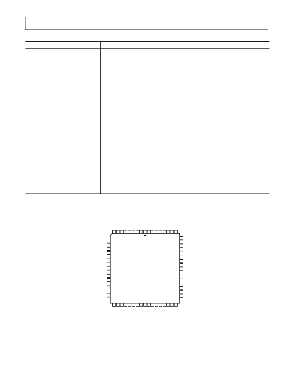
PIN CONFIGURATION
68-Lead Ceramic Leaded Chip Carrier
10
11
12
13
14
15
16
17
18
19
20
22
23
24
25
26
21
27
43
28 29 30 31 32 33 34 35 36 37 38 39 40 41 42
9
61
8
7
6
5
68 67 66 65 64 63 62
4
3
2
1
60
59
58
57
56
55
54
53
52
51
50
49
48
47
46
45
44
TOP VIEW
(Not to Scale)
GNDB
GNDB
GNDB
NC
NC
NC
GNDB
GNDB
ENCODEB
ENCODEB
DV
CC
D11B (MSB)
D10B
D9B
D8B
D7B
GNDB
GNDA
DV
CC
D9A
D10A
(MSB) D11A
ENCODEA
ENCODEA
NC
NC
D1B
D2B
D3B
D4B
D5B
D6B
GNDB
(LSB) D0B
GNDA
GNDA
NC
AV
EE
AV
CC
NC
NC
(LSB) D0A
D1A
D2A
D3A
D4A
D5A
D6A
D7A
D8A
GNDA
NC = NO CONNECT
GNDA
GNDB
GNDA
A
IN
A1
GNDA
NC
NC
AV
EE
A
IN
B3
AV
CC
GNDB
A
IN
A3
A
IN
A2
GNDB
A
IN
B1
A
IN
B2
SHIELD
AD10265
PIN 1