 | –≠–ª–µ–∫—Ç—Ä–æ–Ω–Ω—ã–π –∫–æ–º–ø–æ–Ω–µ–Ω—Ç: AD10680 | –°–∫–∞—á–∞—Ç—å:  PDF PDF  ZIP ZIP |
Document Outline
- ˛ˇ
- ˛ˇ
- ˛ˇ
- FUNCTIONAL BLOCK DIAGRAM
- ˛ˇ
- ˛ˇ
- ˛ˇ
- ˛ˇ
- ˛ˇ
- ˛ˇ
16-Bit, 100 MSPS A/D Converter
Preliminary Technical Data
AD10680
Rev. PrA
Information furnished by Analog Devices is believed to be accurate and reliable. However, no
responsibility is assumed by Analog Devices for its use, nor for any infringements of patents or other
rights of third parties that may result from its use. Specifications subject to change without notice. No
license is granted by implication or otherwise under any patent or patent rights of Analog Devices.
Trademarks and registered trademarks are the property of their respective owners.
One Technology Way, P.O. Box 9106, Norwood, MA 02062-9106, U.S.A.
Tel: 781.329.4700
www.analog.com
Fax: 781.461.3113
©2006 Analog Devices, Inc. All rights reserved.
FEATURES
100 MSPS sample rate
SNR of 85 dBFS @10 MHz
SFDR of 85 dBFS @10 MHz
VSWR of 1:1.5
AC-coupled input signal conditioning
Enhanced signal-to-noise ratio
Differential ENCODE signal
LVDS output levels
Twos complement output data
APPLICATIONS
Communications test equipment
Radar and satellite subsystems
Phased array antennas--digital beams
Multichannel, multimode receivers
Secure communications
Wireless and wired communications
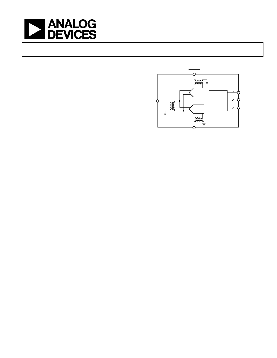
GENERAL DESCRIPTION
The AD10680 is a 16-bit analog-to-digital converter (ADC)
with a transformer-coupled, analog input and digital
postprocessing for enhanced signal-to-noise ratio (SNR). The
product operates at a 100 MSPS conversion rate with
outstanding dynamic performance. Internal filters can be
digitally selected for the appropriate bandwidth or externally
programmed.
The AD10680 requires 5.0 V analog, 3.3 V analog, 3.3 V digital,
2.5 V digital, and a 1.2V digital supply, and a differential encode
signal. No external reference is required.
Performance is rated over a 0∞C to 60∞C case temperature range.
FUNCTIONAL BLOCK DIAGRAM
ADC
A
ADC
B
AD10680
ENCODE
ENCODE
2
32
2
OVER RANGE
DIGITAL
POST
PROCESSING
D0 TO D15
DATA CLOCK
OUTPUT
A
IN
06188-
001
Figure 1.
PRODUCT HIGHLIGHTS
1.
Guaranteed sample rate up to 100 MSPS.
2.
Input signal conditioning with optimized dynamic
performance to 40 MHz.
3.
Additional performance options are available, such as
increased SNR performance with digitally selectable input
bandwidths, digitally selectable full-scale input ranges, and
digitally selectable Nyquist zones. Contact sales for more
information.

AD10680
Preliminary Technical Data
Rev. PrA | Page 2 of 8
TABLE OF CONTENTS
Features .............................................................................................. 1
Applications....................................................................................... 1
General Description ......................................................................... 1
Functional Block Diagram .............................................................. 1
Product Highlights ........................................................................... 1
Revision History ............................................................................... 2
Specifications..................................................................................... 3
DC Specifications ......................................................................... 3
AC Specifications ..........................................................................4
Pin Configurations and Function Descriptions ............................5
Theory of Operation .........................................................................6
Input Stage......................................................................................6
Encoding the AD10680 ................................................................6
Analog and Digital Power Supplies.............................................6
Analog and Digital Grounding....................................................6
REVISION HISTORY
6/06--Revision PrA: Initial Version

Preliminary Technical Data
AD10680
Rev. PrA | Page 3 of 8
SPECIFICATIONS
DC SPECIFICATIONS
AVDD1 = 3.3 V, AVDD2 = 5.0 V, DRVDD1 = 1.2 V, DRVDD2 = 2.5 V, DRVDD3 = 3.3 V, ENCODE = 100 MSPS, unless otherwise noted.
Table 1.
AD10680KWS
Parameter Case
Temp
Test
Level
Min
Typ
Max
Unit
RESOLUTION
12
Bits
ACCURACY
No Missing Codes
IV
Guaranteed
Offset
Error
60∞C
I
±7
LSB
Gain Error @ 10 MHz
60∞C
I
±0.6
%FS
Differential Nonlinearity (DNL)
60∞C
V
TBD
LSB
Integral Nonlinearity (INL)
60∞C
V
TBD
LSB
TEMPERATURE
DRIFT
Gain
Error
60∞C
V
TBD
%/∞C
ANALOG
INPUT
(AIN)
Full-Scale Input Voltage Range
60∞C
V
2.2
V p-p
Frequency Range
Full
IV
5
45
MHz
Flatness (5 MHz to 45MHz)
Full
IV
0.5
1.5
dB
Input VSWR (50 )
(300 KHz to 50 MHz)
60∞C
V
1.5
Analog Input Bandwidth
60∞C
V
100
MHz
POWER
SUPPLY
Supply
Voltage
AVDD1
Full
IV
3.3
V
AVDD2
Full
IV
5.0
V
DRVDD1
Full
IV
1.2
V
DRVDD2
Full
IV
2.5
V
DRVDD3
Full
IV
3.3
V
Supply
Current
I
AVDD1
(AVDD1 = 3.3 V)
60∞C
I
750
mA
I
AVDD2
(AVDD2 = 5.0 V)
60∞C
I
450
mA
I
DRVDD1
(DRVDD1 = 1.2 V)
60∞C
I
600
mA
I
DRVDD2
(DRVDD2 = 2.5 V)
60∞C
I
500
mA
I
DRVDD3
(DRVDD3 = 3.3 V)
60∞C
I
140
mA
Total Power Dissipation
60∞C
I
7.15
W
ENCODE
INPUTS
Differential Inputs (ENC, ENC)
Input Voltage Range
Full
IV
0.4
V
Input
Resistance
60∞C
V
100
Input
Capacitance
60∞C
V
4
pF
Common-Mode
Voltage
60∞C
V
±3
V
LOGIC INPUTS (RESET)
Logic 1 Voltage
Full
IV
2.0
V
Logic 0 Voltage
Full
IV
0.8
V
Source I
IH
60∞C
V
10
A
Source I
IL
60∞C
V
1
mA
LOGIC OUTPUTS (DRA, Output Bits)
Differential
Output
Voltage
Full
IV
247
454 mV
Output Drive Current
Full
IV
-4
+4
mA
Output Common-Mode Voltage
Full
IV
1.125
1.375
V
Start-Up
Time
Full
IV
600
ms

AD10680
Preliminary Technical Data
Rev. PrA | Page 4 of 8
AC SPECIFICATIONS
AVDD1 = 3.3 V, AVDD2 = 5.0 V, DRVDD1 = 1.2 V, DRVDD2 = 2.5 V, DRVDD3 = 3.3 V, ENCODE = 100 MSPS, unless otherwise noted.
Table 2.
AD10680KWS
Parameter Conditions
Case
Temp
Test
Level
Min
Typ
Max
Unit
DYNAMIC PERFORMANCE
SNR
Analog Input
10 MHz
60∞C
I
TBD
85
dBFS
@ -1.0 dBFS
30 MHz
60∞C
I
TBD
84.5
dBFS
40
MHz
Full
V
83.5
dBFS
SINAD
Analog Input
10 MHz
60∞C
I
TBD
84
dBFS
@ -1.0 dBFS
30 MHz
60∞C
I
TBD
83.5
dBFS
40
MHz
Full
V
83
dBFS
Spurious-Free Dynamic Range
Analog Input
10 MHz
60∞C
I
TBD
85
dBFS
@ -1.0 dBFS
30 MHz
60∞C
I
TBD
83
dBFS
40
MHz
Full
V
83
dBFS
Two-Tone IMD
1
F1, F2 @ -6 dBFS
60∞C
V
-75
dBc
SWITCHING SPECIFICATIONS
Conversion Rate
Full
IV
100
MSPS
ENCODE Pulse Width High (t
EH
)
60∞C
V
5
ns
ENCODE Pulse Width Low (t
EL
)
60∞C
V
5
ns
DIGITAL OUTPUT PARAMETERS
Valid Time (t
V
)
Full
IV
TBD
ns
Propagation Delay (t
PD
) 60∞C
V
TBD
ns
Rise Time (t
R
)
(20% to 80%)
60∞C
V
TBD
ns
Fall Time (t
F
)
(20% to 80%)
60∞C
V
TBD
ns
DR PROPAGATION DELAY (t
EDR
)
60∞C
V
TBD
ns
Data to DR Skew (t
EDR
- t
PD
)
60∞C
V
TBD
ns
Pipeline Latency
2
Full
IV
TBD
Cycles
Aperture Delay (t
A
)
60∞C
V
TBD
ns
Aperture Uncertainty (Jitter, t
J
)
60∞C V
TBD
ps
rms
1
F1 = 10 MHz, F2 = 12 MHz.
2
Pipeline latency is exactly TBD cycles.
Preliminary Technical Data
AD10680
Rev. PrA | Page 5 of 8
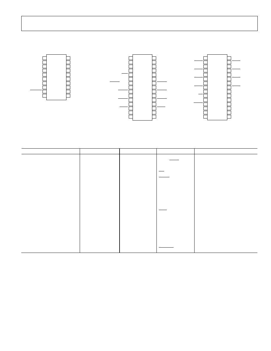
PIN CONFIGURATIONS AND FUNCTION DESCRIPTIONS
06
18
8-
00
2
AD10680
TOP VIEW
(Not to Scale)
AGND
1
AGND
2
3.3V
3
AIN
4
3.3V
5
AGND
6
AGND
7
AGND
8
5.0V
9
AGND
10
5.0V
11
AGND
12
AGND
13
AGND
14
ENCODE
15
AGND
16
ENCODE
17
AGND
18
AGND
19
AGND
20
Figure 2. Pin Configuration P1
06
18
8-
00
3
AD10680
TOP VIEW
(Not to Scale)
NC
1
NC
2
NC
3
NC
4
DGND
5
1.2VD
6
DCO
7
1.2VD
8
DCO
9
1.2VD
10
D
OUT
15 (MSB)
11
D
OUT
14
12
D
OUT
15 (MSB)
13
D
OUT
14
14
D
OUT
13
15
D
OUT
12
16
D
OUT
13
17
D
OUT
12
18
D
OUT
11
19
D
OUT
10
20
D
OUT
11
21
D
OUT
10
22
D
OUT
9
23
D
OUT
8
24
D
OUT
9
25
D
OUT
8
26
NC
27
DGND
28
NC
29
DGND
30
NC = NO CONNECT
Figure 3. Pin Configuration P2
06
18
8-
0
04
AD10680
TOP VIEW
(Not to Scale)
D
OUT
7
1
D
OUT
6
2
D
OUT
7
3
D
OUT
6
4
D
OUT
5
5
D
OUT
4
6
D
OUT
5
7
D
OUT
4
8
D
OUT
3
9
D
OUT
2
10
D
OUT
3
11
D
OUT
2
12
D
OUT
1
13
D
OUT
0 (LSB)
14
D
OUT
1
15
D
OUT
0 (LSB)
16
OR
17
DGND
18
OR
19
DGND
20
3.3VD
21
2.5VD
22
RESET
23
2.5VD
24
NC
25
NC
26
NC
27
NC
28
NC
29
NC
30
Figure 4. Pin Configuration P3
Table 3. Pin Function Descriptions
P1 Pin No.
1
P2 Pin No.
2
P3 Pin No.
3
Mnemonic Description
N/A
5, 28, 30
18, 20
DGND
Digital Ground
N/A
11 to 26
1 to 16
D
OUT
x, D
OUT
x
Data Bit Output, Complement
N/A N/A
17
OR
Overrange
N/A N/A
19
OR
Overrange, Complement
N/A N/A
23
RESET
Reset
N/A
6, 8, 10
N/A
1.2VD
Digital Voltage
N/A N/A
22,
24
2.5VD
Digital
Voltage
N/A N/A
21
3.3VD
Digital
Voltage
(V
DD
)
N/A
1 to 4, 27, 29
25 to 30
NC
No Connection
N/A
7
N/A
DCO
Data Clock Output
N/A 9
N/A
DCO
Data Clock Output, Complement
3, 5
N/A
N/A
3.3V
Encode Voltage (EV
CC
)
9, 11
N/A
N/A
5.0V
Analog Voltage (AV
CC
)
1, 2, 6, 7, 8, 10, 12,
13, 14, 16, 18, 19, 20
N/A N/A
AGND
Analog
Ground
4 N/A
N/A
AIN
Analog
Input
15 N/A
N/A
ENCODE
ENCODE
Input
17 N/A
N/A
ENCODE
ENCODE Input, Complement
1
Equivalent pin configuration is J1.
2
Equivalent pin configuration is J2.
3
Equivalent pin configuration is J3.

AD10680
Preliminary Technical Data
Rev. PrA | Page 6 of 8
THEORY OF OPERATION
The AD10680 uses two, high speed 16 bit ADCs with an
interleaved-averaging algorithm to improve the SNR. The
AD10680 is optimized for a 40 MHz bandwidth centered in the
first Nyquist zone. The AD10680 provides a single-ended,
analog input pin with a full-scale input range of 2.2 V p-p. The
analog input is designed for 50 input impedance. The
AD10680's differential ENCODE inputs are ac-coupled and
internally supplied to the two16 bit ADCs. The digital outputs
from the two ADCs are applied to the field-programmable gate
array (FPGA) for postprocessing. The result is a 16-bit parallel
LVDS word coded as twos complement.
INPUT STAGE
The user is provided with a single-to-differential, transformer-
coupled input. The input impedance is 50 and requires a
2.2 V p-p input level to achieve full scale.
ENCODING THE AD10680
The AD10680's differential ENCODE signal must be a high
quality, low phase noise source to prevent performance
degradation. The clock input must be treated as an analog input
signal because aperture jitter can affect dynamic performance.
For optimum performance, the AD10680 must be clocked
differentially.
ANALOG AND DIGITAL POWER SUPPLIES
Care must be taken when selecting a power source. Linear
supplies are recommended. Switching supplies tend to have
radiated components that can be coupled into the ADCs. The
AD10680 features separate analog and digital supply and
ground currents, helping to minimize digital corruption of
sensitive analog signals.
The 3.3 V digital supply provides power to the digital output
section of the ADCs. The 1.2 V and 2.5 V digital supplies
provide power for the FPGA. The digital supplies should be
decoupled to digital ground (DGND).
The 5.0 V and 3.3 V analog supplies provide power to the
analog sections of the ADCs. Decoupling capacitors are
strategically placed throughout the circuit to provide low
impedance noise shunts to ground. The analog supplies should
be decoupled to analog ground (AGND).
ANALOG AND DIGITAL GROUNDING
Although the AD10680 provides separate analog and digital
ground pins, the device should be treated as an analog
component. Proper grounding is essential in high speed, high
resolution systems. Multilayer printed circuit boards (PCBs) are
recommended to provide optimal grounding and power
distribution. The use of power and ground planes provides
distinct advantages. Power and ground planes minimize the
loop area encompassed by a signal and its return path,
minimize the impedance associated with power and ground
paths, and provide a distributed capacitor formed by the power
plane, printed circuit board material, and ground plane. The
AD10680 unit has five metal standoffs used to fasten the
AD10680 to the customer's PCB. The AD10680 pin connections
mate to a connector (FSI-115-06-L-D-AD-TR for J2 and J3 and
FSI-110-06-L-D-AD-TR for J1).

Preliminary Technical Data
AD10680
Rev. PrA | Page 7 of 8
NOTES

AD10680
Preliminary Technical Data
Rev. PrA | Page 8 of 8
NOTES
©2006 Analog Devices, Inc. All rights reserved. Trademarks and
registered trademarks are the property of their respective owners.
PR06188-0-6/06(PrA)