 | –≠–ª–µ–∫—Ç—Ä–æ–Ω–Ω—ã–π –∫–æ–º–ø–æ–Ω–µ–Ω—Ç: AD1376J | –°–∫–∞—á–∞—Ç—å:  PDF PDF  ZIP ZIP |

REV. B
Information furnished by Analog Devices is believed to be accurate and
reliable. However, no responsibility is assumed by Analog Devices for its
use, nor for any infringements of patents or other rights of third parties
which may result from its use. No license is granted by implication or
otherwise under any patent or patent rights of Analog Devices.
a
AD1376/AD1377
One Technology Way, P.O. Box 9106, Norwood, MA 02062-9106, U.S.A.
Tel: 617/329-4700
World Wide Web Site: http://www.analog.com
Fax: 617/326-8703
© Analog Devices, Inc., 1997
Complete, High Speed
16-Bit A/D Converters
FUNCTIONAL BLOCK DIAGRAM
PRODUCT DESCRIPTION
The AD1376/AD1377 are high resolution, 16-bit analog-to-
digital converters with internal reference, clock and laser-trim-
med thin-film applications resistors. They are packaged in a
compact 32-pin, ceramic scam sealed (hermetic) dual-in-line
packages (DIP). Thin-film scaling resistors provide bipolar
input ranges of
±
2.5 V,
±
5 V,
±
10 V and unipolar input ranges
of 0 V to +5 V, 0 V to +10 V and 0 V to +20 V.
Digital output data is provided in parallel and serial form with
corresponding clock and status outputs. All digital inputs and
outputs are TTL compatible.
APPLICATIONS
The AD1376/AD1377 are excellent for use in high resolution
applications requiring moderate speed and high accuracy or
FEATURES
Complete 16-Bit Converters with Reference and Clock
0.003% Maximum Nonlinearity
No Missing Codes to 14 Bits over Temperature
Fast Conversion
17 s to 16 Bits (AD1376)
10 s to 16 Bits (AD1377)
Short Cycle Capability
Adjustable Clock Rate
Parallel and Serial Outputs
Low Power: 645 mW Typical (AD1376)
585 mW Typical (AD1377)
Industry Standard Pinout
stability over commercial (0
∞
C to +70
∞
C) temperature ranges
(for extended temperature ranges, the pin compatible AD1378
is recommended.) Typical applications include medical and
analytic instrumentation, precision measurement for industrial
robotics, automatic test equipment (ATE), and multichannel
data acquisition systems, servo control systems or anywhere
wide dynamic range is required A proprietary monolithic DAC
and laser-trimmed thin-film resistors guarantee a maximum
nonlinearity of
±
0 003% (1/2 LSB
14
.) The converters may be
short cycled to achieve faster conversion times ≠ 15
µ
s to 14 bits
for the AD1376, or 8
µ
s to 14 bits for the AD1377.
PRODUCT HIGHLIGHTS
1. The AD1376/AD1377 provides 16-bit resolution with a maxi-
mum linearity error of
±
0.003% (1/2 LSB
14
) at +25
∞
C.
2. AD1376 conversion time is 14
µ
s (typical) short cycled to 14
bits, and 16
µ
s to 16 bits.
3. AD1377 conversion time is 8
µ
s (typical) short cycled to 14
bits, and 9
µ
s to 16 bits.
4. Two binary codes are available on the digital output. They are
CSB (Complementary Straight Binary) for unipolar input
voltage ranges and COB (Complementary Offset Binary) for
bipolar input ranges. Complementary Twos Complement
(CTC) coding may be obtained by inverting Pin 1 (MSB).
5. The AD1376 and AD1377 include internal reference and
clock, with external clock rate adjust pin, and serial and paral-
lel digital outputs.

≠2≠
REV. B
AD1376/AD1377≠SPECIFICATIONS
Model
AD1376JD/AD1377JD
AD1376KD/AD1377KD
Units
RESOLUTION
16 (max)
16 (max)
Bits
ANALOG INPUTS
Voltage Ranges
Bipolar
±
2.5,
±
5,
±
10
±
2.5,
±
5,
±
10
Volts
Unipolar
0 to +5, 0 to +10, 0 to +20
0 to +5, 0 to +10, 0 to +20
Volts
Impedance (Direct Input)
0 V to +5 V,
±
2.5 V
1.88
1.88
k
0 V to +10 V,
±
5.0 V
3.75
3.75
k
0 V to +20 V,
±
10 V
7.50
7.50
k
DIGITAL INPUTS
1
Convert command
Positive Pulse 50 ns Wide (min) Trailing Edge Initiates Conversion
Logic Loading
1
1
LS TTL Load
TRANSFER CHARACTERISTICS
2
ACCURACY
Gain Error
±
0.05
3
(
±
0.2 max)
±
0.05
3
(
±
0.2 max)
%
Offset Error
Unipolar
±
0.05
3
(
±
0.1 max)
±
0.05
3
(
±
0.1 max)
% of FSR
4
Bipolar
±
0.05
3
(
±
0.2 max)
±
0.05
3
(
±
0.2 max)
% of FSR
Linearity Error (max)
±
0.006
±
0.003
% of FSR
Inherent Quantization Error
±
1/2
±
1/2
LSB
Differential Linearity Error
±
0.003
±
0.003
% of FSR
POWER SUPPLY SENSITIVITY
±
15 V dc (
±
0.75 V)
0.0015
0.0015
% of FSR/%
V
S
+5 V dc (
±
0.25 V)
0.001
0.001
% of FSR/%
V
S
CONVERSION TIME
5
12 Bits (AD1376)
11.5 (13 max)
11.5 (13 max)
µ
s
14 Bits (AD1376)
13.5 (15 max)
13.5 (15 max)
µ
s
16 Bits (AD1376)
15.5 (17 max)
15.5 (17 max)
µ
s
14 Bits (AD1377)
8.75 max
8.75 max
µ
s
16 Bits (AD1377)
10 max
10 max
µ
s
POWER SUPPLY REQUIREMENTS
Rated Voltage, Analog
±
15,
±
0.5 (max)
±
15,
±
0.5 (max)
V dc
Rated Voltage, Digital
+5,
±
0.25 (max)
+5,
±
0.25 (max)
V dc
AD1376 Power Consumption
645 (850 max)
645 (850 max)
mW
+15 V Supply Drain
+16
+16
mA
≠15 V Supply Drain
≠21
≠21
mA
+5 V Supply Drain
+18
+18
mA
AD1377 Power Consumption
600 (800 max)
600 (800 max)
mW
+15 V Supply Drain
+10
+10
mA
≠15 V Supply Drain
≠23
≠23
mA
+5 V Supply Drain
+18
+18
mA
WARM-UP TIME
1
1
minutes
DRIFT
6
Gain
±
15 (max)
±
5 (
±
15 max)
ppm/
∞
C
Offset
Unipolar
±
2 (
±
4 max)
±
2 (
±
4 max)
ppm of FSR/
∞
C
Bipolar
±
10 (max)
±
3 (
±
10 max)
ppm of FSR/
∞
C
Linearity
±
2 (
±
3 max)
±
0.3 (
±
2 max)
ppm of FSR/
∞
C
Guaranteed No Missing Code
Temperature Range
0 to 70 (13 Bits)
0 to 70 (14 Bits)
∞
C
DIGITAL OUTPUT
1
(All Codes Complementary)
Parallel & Serial
Output Codes
7
Unipolar
CSB
CSB
Bipolar
COB, CTC
8
COB, CTC
8
Output Drive
5
5
LSTTL Loads
(typical at T
A
= +25 C, V
S
= 15, +5 V unless otherwise noted)

≠3≠
REV. B
AD1376/AD1377
ABSOLUTE MAXIMUM RATINGS*
Supply Voltage . . . . . . . . . . . . . . . . . . . . . . . . . . . . . . . .
±
18 V
Logic Supply Voltage . . . . . . . . . . . . . . . . . . . . . . . . . . . . +7 V
Analog Inputs (Pins 24 and 25) . . . . . . . . . . . . . . . . . . .
±
25 V
Analog Ground-to-Digital Ground . . . . . . . . . . . . . . .
±
0.3 V
Digital Inputs . . . . . . . . . . . . . . . . . . . ≠0.3 V to V
DD
+ 0.3 V
Junction Temperature . . . . . . . . . . . . . . . . . . . . . . . . . +175
∞
C
Storage . . . . . . . . . . . . . . . . . . . . . . . . . . . . . . . . . . . . .+15
∞
C
Lead Temperature (10 seconds) . . . . . . . . . . . . . . . . . +300
∞
C
*Absolute maximum ratings are limiting values to be applied individually, and
beyond which the service ability of the circuit may be impaired. Functional
operability is not necessarily implied. Exposure to absolute maximum rating
conditions for an extended period of time may affect device reliability.
ORDERING GUIDE
Maximum Conversion
Temperature
Linearity
Time
Package
Model
Range
Error
(16 Bits)
Option*
AD1376JD
0
∞
C to +70
∞
C
±
0.006%
17
µ
s
DH-32E
AD1376KD 0
∞
C to +70
∞
C
±
0.003%
17
µ
s
DH-32E
AD1377JD
0
∞
C to -70
∞
C
±
0.006%
10
µ
s
DH-32E
AD1377KD 0
∞
C to +70
∞
C
±
0.003%
10
µ
s
DH-32E
*DH-32E = Ceramic DIP.
Model
AD1376JD/AD1377JD
AD1376KD/AD1377KD
Units
Status
Logic "1" During Conversion
Status Output Drive
5 (max)
5 (max)
LSTTL Loads
Internal Clock
9
Clock Output Drive
5 (max)
5 (max)
LSTTL Loads
Frequency
1040/1750
1040/1750
kHz
TEMPERATURE RANGE
Specification
0 to ≠70
0 to ≠70
∞
C
Operating
≠25 to +85
≠25 to +85
∞
C
Storage
≠55 to +125
≠55 to +125
∞
C
NOTES
1
Logic "0" = 0.8 V, max. Logic "1" = 2.0 V, min for inputs. For digital outputs Logic "0" = +0.4 V max. Logic "1" = 2.4 V min.
2
Tested on
±
10 V and 0 V to +10 V ranges.
3
Adjustable to zero.
4
Full-Scale Range.
5
Guaranteed but not 100% production tested.
6
Conversion time may be shortened with "Short Cycle" set for lower resolution.
7
CSB≠Complementary Straight Binary. COB≠Complementary Offset Binary. CTC≠Complementary Twos Complement.
8
CTC coding obtained by inverting MSB (Pin 1).
9
With Pin 23, clock rate controls tied to digital ground.
Specifications subject to change without notice.
Figure 1. Linearity Error vs. Temperature
Figure 2. AD1376 Nonlinearity vs. Conversion Time
Figure 3. Gain Drift Error vs. Temperature
AD1376/AD1377
≠4≠
REV. B
DESCRIPTION OF OPERATION
On receipt of a CONVERT START command, the AD1376/
AD1377 converts the voltage at its analog input into an equiva-
lent 16-bit binary number. This conversion is accomplished as
follows: the 16-bit successive-approximation register (SAR) has
its 16-bit outputs connected both to the device bit output pins
and to the corresponding bit inputs of the feedback DAC. The
analog input is successively compared to the feedback DAC
output, one hit at a time (MSB first, LSB last). The decision to
keep or reject each bit is then made at the completion of each
bit comparison period, depending on the state of the compara-
tor at that time.
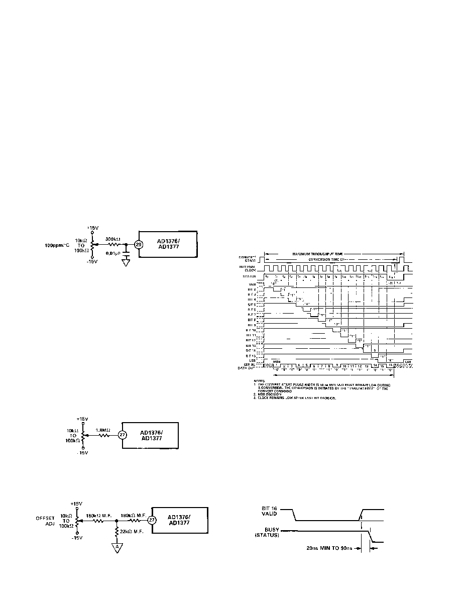
GAIN ADJUSTMENT
The gain adjust circuit consists of a 100 ppm/
∞
C potentiometer
connected across
±
V
S
with its slider connected through a
300 k
resistor to the gain adjust Pin 29 as shown in Figure 4.
If no external trim adjustment is desired, Pin 27 (offset adj) and
Pin 29 (gain adj) may be left open.
Figure 4. Gain Adjustment Circuit (
±
0.2% FSR)
OFFSET ADJUSTMENT
The zero adjust circuit consists of a 100 ppm/
∞
C potentiometer
connected across
±
V
S
with its slider connected through a
1.8 M
resistor to Comparator Input Pin 27 for all ranges. As
shown in Figure 5, the tolerance of this fixed resistor is not
critical, and a carbon composition type is generally adequate.
Using a carbon composition resistor having a ≠1200 ppm/
∞
C
tempco contributes a worst-case offset tempco of 32 LSB
14
61 ppm/LSB
14
1200 ppm/
∞
C = 2.3 ppm/
∞
C of FSR, if the
OFFSET ADJ potentiometer is set at either end of its adjust-
ment range. Since the maximum offset adjustment required is
typically no more than
±
16 LSB
14
, use of a carbon composition
offset summing resistor typically contributes no more than
1 ppm/
∞
C of FSR offset tempco.
Figure 5. Offset Adjustment Circuit (
±
0.3% FSR)
An alternate offset adjust circuit, which contributes negligible
offset tempco if metal film resistors (tempco <100 ppm/
∞
C) are
used, is shown in Figure 6.
Figure 6. Low Tempco Zero Adjustment Circuit
In either adjust circuit, the fixed resistor connected to Pin 27
should be located close to this pin to keep the pin connection
runs short. Comparator Input Pin 27 is quite sensitive to exter-
nal noise pick-up and should be guarded by analog common.
TIMING
The timing diagram is shown in Figure 7. Receipt of a CON-
VERT START signal sets the STATUS flag, indicating conver-
sion in progress. This, in turn, removes the inhibit applied to
the gated clock, permitting it to run through 17 cycles. All the
SAR parallel bits, STATUS flip-flops, and the gated clock in-
hibit signal are initialized on the trailing edge of the CONVERT
START signal. At time t
0
, B
1
is reset and B
2
≠B
16
are set uncon-
ditionally. At t
1
the Bit 1 decision is made (keep) and Bit 2 is
reset unconditionally. This sequence continues until the Bit 16
(LSB) decision (keep) is made at t
16
. The STATUS flag is reset,
indicating that the conversion is complete and that the parallel
output data is valid. Resetting the STATUS flag restores the
gated clock inhibit signal, forcing the clock output to the low
Logic "0" state. Note that the clock remains low until the next
conversion.
Corresponding parallel data bits become valid on the same
positive-going clock edge.
Figure 7. Timing Diagram (Binary Code
0110011101111010)
DIGITAL OUTPUT DATA
Both parallel and serial data from TTL storage registers is in
negative true form (Logic "1" = 0 V and Logic "0" = 2.4 V).
Parallel data output coding is complementary binary for
unipolar ranges and complementary offset binary for bipolar
ranges. Parallel data becomes valid at least 20 ns before the
STATUS flag returns to Logic "0", permitting parallel data
transfer to be clocked on the "1" to "0" transition of the STA-
TUS flag (see Figure 8).
Figure 8. LSB Valid to Status Low
AD1376/AD1377
≠5≠
REV. B
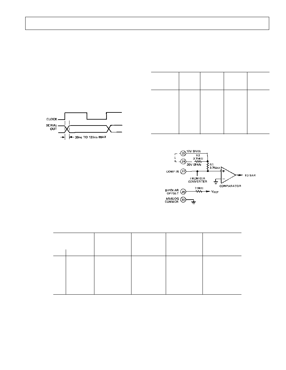
Serial data coding is complementary binary for unipolar input
ranges and complementary offset binary for bipolar input
ranges. Serial output is by bit (1M4SB first, LSB last) in NRZ
(nonreturn-to-zero) format. Serial and parallel data outputs
change state on positive-going clock edges. Serial data is guaran-
teed valid 120 ns after the rising clock edges, permitting serial
data to he clocked directly into a receiving register on the
negative-going clock edges as shown in Figure 9. There are 17
negative-going clock edges in the complete 16-bit conversion
cycle. The first negative edge shifts an invalid bit into the regis-
ter, which is shifted out on the last negative-going clock edge.
All serial data bits will have been correctly transferred and be in
the receiving shift register locations shown at the completion of
the conversion period.
Figure 9. Clock High to Serial Out Valid
Short Cycle Input
A Short Cycle Input, Pin 32, permits the timing cycle shown in
Figure 7 to be terminated after any number of desired bits has
been converted, permitting somewhat shorter conversion times
in applications not requiring full 16-bit resolution. When 10-bit
resolution is desired, Pin 32 is connected to Bit 11 output
Pin 11. The conversion cycle then terminates and the STATUS
flag resets after the Bit 10 decision (timing diagram of Figure 7).
Short cycle connections and associated 8-, 10-, 12-, 13-, 14-
and 15-bit conversion times are summarized in Table I, for a
1.6 MHz clock (AD1377) or 933 kHz (AD1376).
INPUT SCALING
The ADC (ADC) inputs should he scaled as close to the maxi-
mum input signal range as possible in order to utilize the maxi-
mum signal resolution of the A/D converter. Connect the input
signal as shown in Table II. See Figure 10 for circuit details.
Table II. Input Scaling Connections
Input
Connect
Connect
Connect
Signal
Output
Pin 26
Pin 24
Input
Line
Code
to Pin
to
Signal to
±
10 V
COB
27
Input
24
Signal
±
5 V
COB
27
Open
25
±
2.5 V
COB
27
Pin 27
25
0 V to +5 V
CSB
22
Pin 27
25
0 V to +10 V
CSB
22
Open
25
0 V to +20 V
CSB
22
Input
24
Signal
Note
Pin 27 is extremely sensitive to noise and should be guarded by Analog Common.
Figure 10. Input Scaling Circuit
Table I. Short Cycle Connections
Maximum
Maximum
Conversion
Conversion
Connect Short
Resolution
Time≠ s
Time≠ s
Status Flag
Cycle Pin 32 to
Bits
(% FSR)
(AD1377)
(AD1378)
Reset
Pin:
16
0.0015
10
17.1
t
16
NC (Open)
15
0.003
9.4
16.1
t
15
16
14
0.006
8.7
15.0
t
14
15
13
0.012
8.1
13.9
t
13
14
12
0.024
7.5
12.9
t
12
13
10
0.100
6.3
10.7
t
10
11
8
0.390
5.0
8.6
t
8
9