REV. A
Information furnished by Analog Devices is believed to be accurate and
reliable. However, no responsibility is assumed by Analog Devices for its
use, nor for any infringements of patents or other rights of third parties that
may result from its use. No license is granted by implication or otherwise
under any patent or patent rights of Analog Devices. Trademarks and
registered trademarks are the property of their respective companies.
One Technology Way, P.O. Box 9106, Norwood, MA 02062-9106, U.S.A.
Tel: 781/329-4700
www.analog.com
Fax: 781/326-8703
� 2003 Analog Devices, Inc. All rights reserved.
AD15700
1 MSPS 16-/14-Bit
Analog I/O Port
FEATURES
16-Bit A/D Converter
1 MSPS
S/(N + D): 90 dB Typ @ 250 kHz
No Pipeline Delay
14-Bit D/A Converter
Settling Time: 1 s
S/N: 92 dB Typ
2 80 MHz Amplifiers
30 V/ s Slew Rate
Rail-to-Rail Input and Output
Output Current 15 mA
2 Gain Setting Center Tapped Resistors
Resistor Ratio Tracking: 2 ppm/ C
Unipolar Operation
SPI
�
/QSPITM/MICROWIRETM/DSP Compatible
132 mW Typical Power Dissipation
APPLICATIONS
Optical MEMS Mirror Control
Industrial Process Control
Data Acquisition
Instrumentation
Communication
PRODUCT HIGHLIGHTS
1. Fast Throughput ADC.
The AD15700 incorporates a high speed, 1 MSPS, 16-bit
SAR ADC.
2. Superior ADC INL.
The 16-bit ADC has a maximum integral nonlineariy of
2.5 LSB with no missing codes.
3. Two Precision Resistor Networks with 2 ppm/
C Ratio
Tracking for Gain Setting.
4. Low Power Consumption.
Typically 132 mW at maximum performance levels.
5. Industrial Temperature Range: �40
C to +85C.
GENERAL DESCRIPTION
The AD15700 is a precision component to interface analog input
and output channels to a digital processor. It is ideal for area-
limited applications that require maximum circuit density. The
AD15700 contains the functionality of a 16-bit, 1 MSPS charge
redistribution SAR analog-to-digital converter that operates from
a 5 V power supply. The high speed 16-bit sampling ADC incor-
porates a resistor input scaler that allows various input ranges, an
internal conversion clock, error correction circuits, and both serial
and parallel system interface ports. The AD15700 also contains a
14-bit, serial input, voltage output DAC that operates from a 5 V
supply and has a settling time of 1
ms. Two single- or split-supply
voltage feedback amplifiers with rail-to-rail input and output
characteristics featuring 80 MHz of small signal bandwidth and
10
mV/C offset drift provide ADC and DAC buffering capability.
The center tapped 3 k
W resistors are precision resistor networks
with 2 ppm/
C ratio tracking that provide low gain drift when
used for scaling.
The ADC, DAC, and amp functions are electrically isolated from
each other to provide maximum design flexibility. Input and
output signal conditioning circuits for the converters can be easily
configured with short interconnects under the device at the board
level. The AD15700 is available in a 10 mm CSPBGA package.
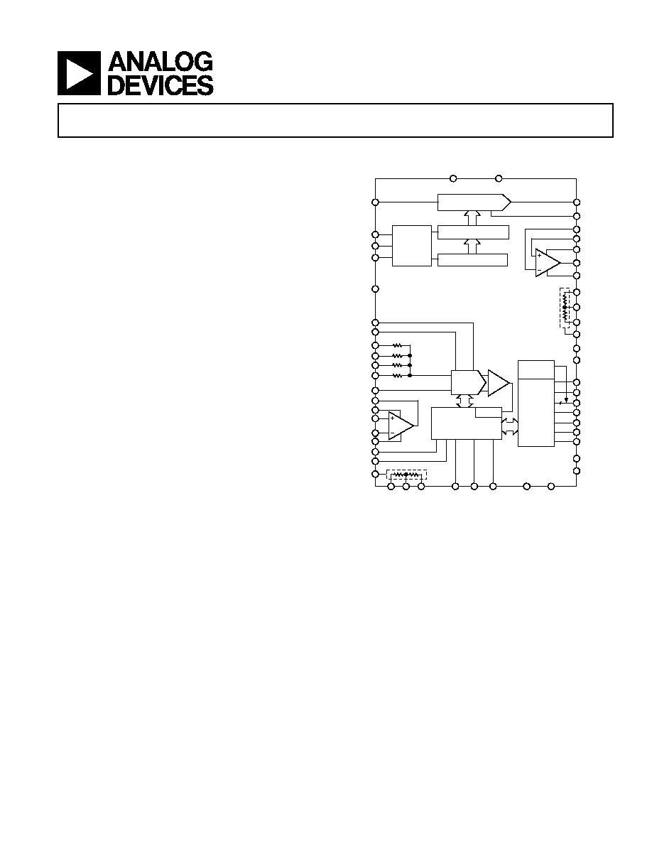
FUNCTIONAL BLOCK DIAGRAM
SERIAL
PORT
PARALLEL
INTERFACE
16
R
2R
4R
4R
SAR ADC
CONTROL LOGIC AND
CALIBRATION CIRCUITRY
CLOCK
SWITCHED
CAP DAC
OVDD
OGND
SER/
PAR
BUSY
D[15:0]
CS_ADC
RD
OB/
2C
BYTESWAP
WARP
IMPULSE
CNVST
AVDD
AGND_ADC
REF
REFGND
DVDD
DGND
ADC
IND(4R)
INC(4R)
INB(2R)
INA(R)
INGND
PD
RESET
SERIAL INPUT REGISTER
14-BIT DATA LATCH
CONTROL
LOGIC
14-BIT DAC
VDD_DAC
DGND_DAC
CS_DAC
DIN
SCLK
VREF
VOUT_DAC
AGND_DAC
�VS2
+VS2
�VS1
+VS1
AD15700
RA1
RB1
RC1
RB2 RC2
RA2
+IN2
�IN2
VOUT2
�IN1
+IN1
VOUT1
RPAD2
RPAD1
COMMON
1.5k
1.5k
1.5k
1.5k

REV. A
�2�
AD15700�SPECIFICATIONS
Parameter
Condition
Min
Typ
Max
Unit
RESOLUTION
16
Bits
ANALOG INPUT
Voltage Range
VIND � VINGND
�4 REF, 0 V to 4 REF, �2 REF (See Table I)
Common-Mode Input Voltage
VINGND
�0.1
+0.5
V
Analog Input CMRR
f
IN
= 100 kHz
74
dB
Input Impedance
See Table I
THROUGHPUT SPEED
Complete Cycle
In Warp Mode
1
ms
Throughput Rate
In Warp Mode
1
1000
kSPS
Time between Conversions
In Warp Mode
1
ms
Complete Cycle
In Normal Mode
1.25
ms
Throughput Rate
In Normal Mode
0
800
kSPS
Complete Cycle
In Impulse Mode
1.5
ms
Throughput Rate
In Impulse Mode
0
666
kSPS
DC ACCURACY
Integral Linearity Error
�2.5
+2.5
LSB
1
No Missing Codes
16
Bits
Transition Noise
0.7
LSB
Bipolar Zero Error
2
, T
MIN
to T
MAX
�5 V Range, Normal or
�45
+45
LSB
Impulse Modes
Other Range or Mode
�0.1%
% of FSR
Bipolar Full-Scale Error
2
, T
MIN
to T
MAX
�0.38
+0.38
% of FSR
Unipolar Zero Error
2
, T
MIN
to T
MAX
�0.18
+0.18
% of FSR
Unipolar Full-Scale Error
2
, T
MIN
to T
MAX
�0.76
+0.76
% of FSR
Power Supply Sensitivity
AVDD = 5 V
� 5%
�9.5
LSB
AC ACCURACY
Signal-to-Noise
f
IN
= 20 kHz
89
90
dB
3
f
IN
= 250 kHz
90
dB
Spurious-Free Dynamic Range
f
IN
= 250 kHz
100
dB
Total Harmonic Distortion
f
IN
= 20 kHz
�100
�96
dB
f
IN
= 250 kHz
�100
dB
Signal-to-(Noise + Distortion)
f
IN
= 20 kHz
88.5
90
dB
f
IN
= 250 kHz, �60 dB Input
30
dB
�3 dB Input Bandwidth
9.6
MHz
SAMPLING DYNAMICS
Aperture Delay
2
ns
Aperture Jitter
5
ps rms
Transient Response
Full-Scale Step
250
ns
REFERENCE
External Reference Voltage Range
2.3
2.5
3.0
V
External Reference Current Drain
1 MSPS Throughput
200
mA
DIGITAL INPUTS
Logic Levels
V
IL
�0.3
+0.8
V
V
IH
+2.0
DVDD + 0.3
V
I
IL
�1
+1
mA
I
IH
�1
+1
mA
16-BIT ADC ELECTRICAL CHARACTERISTICS
(�40 C to +85 C, AVDD = DVDD = 5 V, 0VDD = 2.7 V to 5.25 V, unless
otherwise noted.)

REV. A
AD15700
�3�
Parameter
Condition
Min
Typ
Max
Unit
DIGITAL OUTPUTS
Data Format
Parallel or Serial 16-Bit
Pipeline Delay
Conversion Results Available Immediately
after Completed Conversion
V
OL
I
SINK
= 1.6 mA
0.4
V
V
OH
I
SOURCE
= �570
mA
OVDD � 0.6
V
POWER SUPPLIES
Specified Performance
AVDD
4.75
5
5.25
V
DVDD
4.75
5
5.25
V
OVDD
2.7
5.25
V
Operating Current
4
AVDD
15
mA
DVDD
5
7.2
mA
OVDD
5
37
mA
Power Dissipation
5, 6
666 kSPS Throughput
7
84
95
mW
100 SPS Throughput
7
15
mW
1 MSPS Throughput
4
112
125
mW
In Power-Down Mode
8
1
mW
TEMPERATURE RANGE
Specified Performance
T
MIN
to T
MAX
�40
+85
C
NOTES
1
LSB means Least Significant Bit. With the
�5 V input range, one LSB is 152.588 mV.
2
These specifications do not include the error contribution from the external reference.
3
All specifications in dB are referred to a full-scale input FS. Tested with an input signal at 0.5 dB below full scale, unless otherwise specified.
4
In Warp Mode.
5
Tested in Parallel Reading Mode.
6
Tested with the 0 V to 5 V range and VIN � VINGND = 0 V.
7
In Impulse Mode.
8
With OVDD below DVDD + 0.3 V and all digital inputs forced to OVDD or OGND, respectively.
Specifications subject to change without notice.
Table I. Analog Input Configuration
Input Voltage Range
IND(4R)
INC(4R)
INB(2R)
INA(R)
Input Impedance
1
�4 REF
V
IN
INGND
INGND
REF
1.63 k
W
�2 REF
V
IN
V
IN
INGND
REF
948
W
� REF
V
IN
V
IN
V
IN
REF
711
W
0 V to 4 REF
V
IN
V
IN
INGND
INGND
948
W
0 V to 2 REF
V
IN
V
IN
V
IN
INGND
711
W
0 V to REF
V
IN
V
IN
V
IN
V
IN
Note 2
NOTES
1
Typical analog input impedance.
2
For this range, the input is high impedance.

REV. A
�4�
AD15700
16-BIT ADC TIMING CHARACTERISTICS
(�40 C to +85 C, AVDD = DVDD = 5 V, 0VDD = 2.7 V to 5.25 V, unless otherwise noted.)
Parameter
Symbol
Min
Typ
Max
Unit
Refer to Figures 14 and 15
Convert Pulsewidth
t
1
5
ns
Time between Conversions
t
2
1/1.25/1.5
Note 1
ms
(Warp Mode/Normal Mode/Impulse Mode)
CNVST LOW to BUSY HIGH Delay
t
3
30
ns
BUSY HIGH All Modes Except in Master Serial Read after
t
4
0.75/1/1.25
ms
Convert Mode (Warp Mode/Normal Mode/Impulse Mode)
Aperture Delay
t
5
2
ns
End of Conversion to BUSY LOW Delay
t
6
10
ns
Conversion Time (Warp Mode/Normal Mode/Impulse Mode)
t
7
0.75/1/1.25
ms
Acquisition Time
t
8
1
ms
RESET Pulsewidth
t
9
10
ns
Refer to Figures 16, 17, and 18 (Parallel Interface Modes)
CNVST LOW to DATA Valid Delay
t
10
0.75/1/1.25
ms
(Warp Mode/Normal Mode/Impulse Mode)
DATA Valid to BUSY LOW Delay
t
11
20
ns
Bus Access Request to DATA Valid
t
12
40
ns
Bus Relinquish Time
t
13
5
15
ns
Refer to Figures 20 and 21 (Master Serial Interface Modes)
2
CS_ADC LOW to SYNC Valid Delay
t
14
10
ns
CS_ADC LOW to Internal SCLK Valid Delay
t
15
10
ns
CS_ADC LOW to SDOUT Delay
t
16
10
ns
CNVST LOW to SYNC Delay (Read During Convert)
t
17
25/275/525
ns
(Warp Mode/Normal Mode/Impulse Mode)
SYNC Asserted to SCLK First Edge Delay
3
t
18
4
ns
Internal SCLK Period
3
t
19
25
40
ns
Internal SCLK HIGH
3
t
20
15
ns
Internal SCLK LOW
3
t
21
9
ns
SDOUT Valid Setup Time
3
t
22
4.5
ns
SDOUT Valid Hold Time
3
t
23
2
ns
SCLK Last Edge to SYNC Delay
3
t
24
3
ns
CS_ADC HIGH to SYNC HI-Z
t
25
10
ns
CS_ADC HIGH to Internal SCLK HI-Z
t
26
10
ns
CS_ADC HIGH to SDOUT HI-Z
t
27
10
ns
BUSY HIGH in Master Serial Read after Convert
3
t
28
See Table II
ms
CNVST LOW to SYNC Asserted Delay
t
29
0.75/1/1.25
ms
Master Serial Read after Convert
SYNC Deasserted to BUSY LOW Delay
t
30
25
ns
Refer to Figures 22 and 24 (Slave Serial Interface Modes)
External SCLK Setup Time
t
31
5
ns
External SCLK Active Edge to SDOUT Delay
t
32
3
16
ns
SDIN Setup Time
t
33
5
ns
SDIN Hold Time
t
34
5
ns
External SCLK Period
t
35
25
ns
External SCLK HIGH
t
36
10
ns
External SCLK LOW
t
37
10
ns
NOTES
1
In Warp Mode only, the maximum time between conversions is 1 ms; otherwise, there is no required maximum time.
2
In Serial Interface Modes, the SYNC, SCLK, and SDOUT timings are defined with a maximum load C
L
of 10 pF; otherwise, the load is 60 pF maximum.
3
In serial master Read during Convert Mode. See Table II.
Specifications subject to change without notice.
REV. A
AD15700
�5�
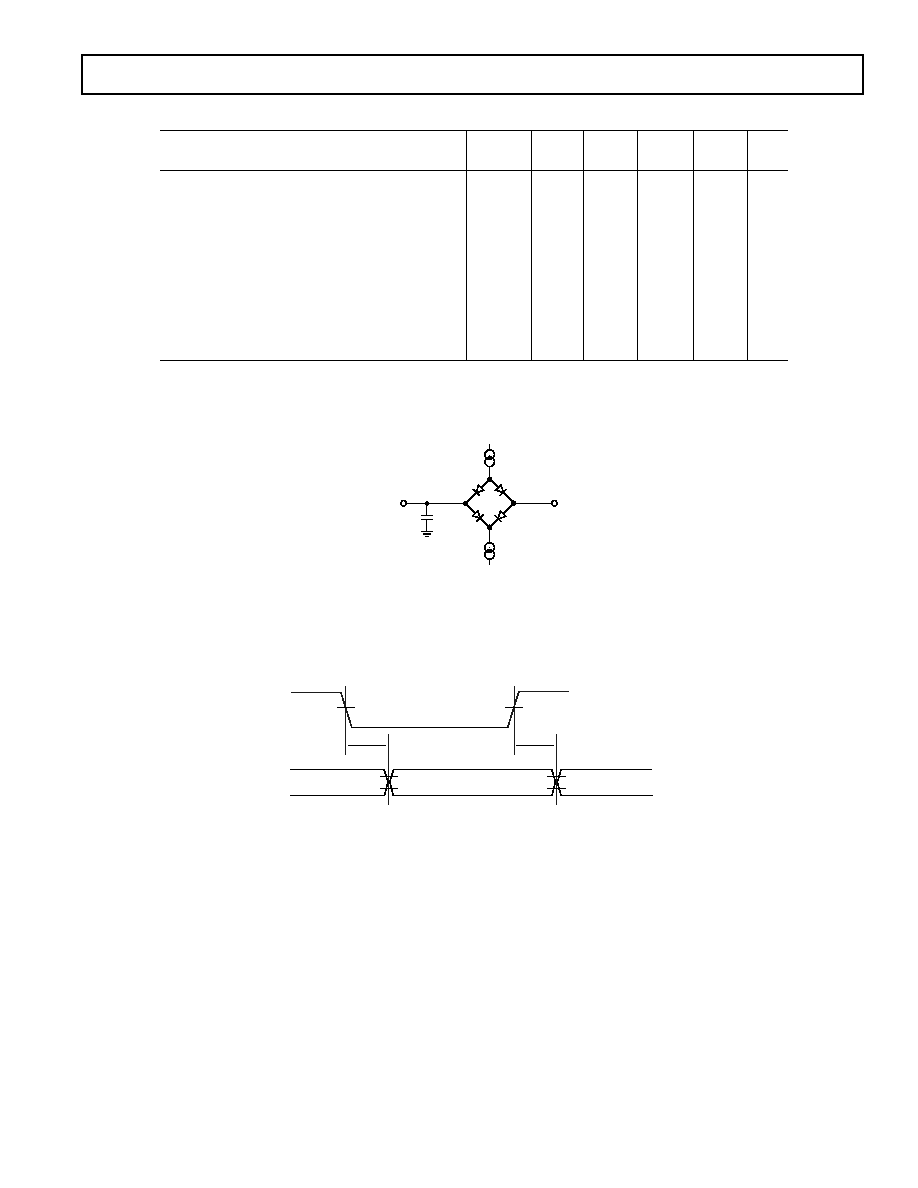
1.6mA
I
OL
I
OH
500mA
C
L
60pF
TO OUTPUT
PIN
IN SERIAL INTERFACE MODES, THE SYNC, SCLK, AND
SDOUT TIMINGS ARE DEFINED WITH A MAXIMUM LOAD
C
L
OF 10pF; OTHERWISE THE LOAD IS 60pF MAXIMUM.
1.4V
Figure 1. Load Circuit for Digital Interface Timing, SDOUT, SYNC, SCLK Outputs, C
L
= 10 pF
0.8V
t
DELAY
2V
t
DELAY
0.8V
2V
2V
0.8V
Figure 2. Voltage Reference Levels for Timing
Table II. Serial Clock Timings in Master Read after Convert
DIVSCLK[1]
0
0
1
1
DIVSCLK[0]
Symbol
0
1
0
1
Unit
SYNC to SCLK First Edge Delay Minimum
t
18
4
20
20
20
ns
Internal SCLK Period Minimum
t
19
25
50
100
200
ns
Internal SCLK Period Maximum
t
19
40
70
140
280
ns
Internal SCLK HIGH Minimum
t
20
15
25
50
100
ns
Internal SCLK LOW Minimum
t
21
9
24
49
99
ns
SDOUT Valid Setup Time Minimum
t
22
4.5
22
22
22
ns
SDOUT Valid Hold Time Minimum
t
23
2
4
30
89
ns
SCLK Last Edge to SYNC Delay Minimum
t
24
3
60
140
300
ns
BUSY HIGH Width Maximum (Warp)
t
28
1.5
2
3
5.25
ms
BUSY HIGH Width Maximum (Normal)
t
28
1.75
2.25
3.25
5.5
ms
BUSY HIGH Width Maximum (Impulse)
t
28
2
2.5
3.5
5.75
ms