 | –≠–ª–µ–∫—Ç—Ä–æ–Ω–Ω—ã–π –∫–æ–º–ø–æ–Ω–µ–Ω—Ç: AD1836AS | –°–∫–∞—á–∞—Ç—å:  PDF PDF  ZIP ZIP |
PRELIMINARY TECHNICAL DATA
REV. PrC
Information furnished by Analog Devices is believed to be accurate and
reliable. However, no responsibility is assumed by Analog Devices for its
use, nor for any infringements of patents or other rights of third parties
which may result from its use. No license is granted by implication or
otherwise under any patent or patent rights of Analog Devices.
a
Preliminary Technical Data AD1836
One Technology Way, P.O. Box 9106, Norwood, MA 02062-9106, U.S.A.
Tel: 781/329-4700
World Wide Web Site: www.analog.com
Fax: 781/326-8703
© Analog Devices, Inc., 2001
Multichannel 96 kHz Codec
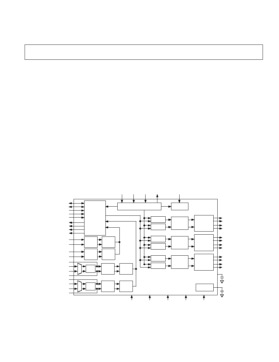
FUNCTIONAL BLOCK DIAGRAM
VOLUME
VOLUME
DIGITAL
FILTER
DAC
A
OUT
1
A
OUT
2
CLOCK
MCLK
COUT
V
REF
FILTD
CONTROL PORT
CCLK
CDATA CLATCH
SERIAL
DATA
I/O
PORT
DIGITAL
FILTER
48/96kHz
ADC1L
48/96kHz
DIGITAL
FILTER
48/96kHz
ADC1R
48/96kHz
MUX
PGA
ADC2L
48kHz
DIGITAL
FILTER
48kHz
DLRCLK
DBCLK
DSDATA1
DSDATA2
DSDATA3
ALRCLK
ABCLK
ASDATA1
ASDATA2
A
IN
1L
CAPL1
A
IN
2L1
A
IN
2L2
CAPL2
CAPR1
CAPR2
A
IN
2R1
A
IN
2R2
PWRDWN/RESET
AVDD
AGND
DVDD
DGND
2
4
3
2
MUX
PGA
ADC2R
48kHz
DIGITAL
FILTER
48kHz
A
IN
1R
VOLUME
VOLUME
DIGITAL
FILTER
DAC
A
OUT
3
A
OUT
4
VOLUME
VOLUME
DIGITAL
FILTER
DAC
A
OUT
5
A
OUT
6
FILTR
FEATURES
5 V Multichannel Audio System
Accepts 16-/18-/20-/24-Bit Data
Supports 24 Bits and 96 kHz Sample Rate
Multibit Sigma-Delta Modulators with Data Directed
Scrambling
Data-Directed Scrambling ADCs and DACs--Least
Sensitive to Jitter
Differential Output for Optimum Performance
ADCs: ≠92 dB THD + N, 105 dB SNR and Dynamic Range
DACs: ≠95 dB THD + N, 108 dB SNR and Dynamic Range
On-Chip Volume Control with "Autoramp" Function
Programmable Gain Amplifier for ADC Input
Hardware and Software Controllable Clickless Mute
Digital De-Emphasis Processing
Supports 256 f
S
, 512 f
S,
or 768 f
S
Master Clock
Power-Down Mode Plus Soft Power-Down Mode
Flexible Serial Data Port with Right-Justified, Left-
Justified, I
2
S-Compatible and DSP Serial Port Modes
TDM Interface Mode Supports 8 In/8 Out Using a
Single SHARC
Æ
SPORT
52-Lead MQFP (PQFP) Plastic Package
GENERAL DESCRIPTION
The AD1836 is a high-performance, single-chip codec pro-
viding three stereo DACs and two stereo ADCs using ADI's
patented multibit sigma-delta architecture. An SPI port is
included, allowing a microcontroller to adjust volume and
many other parameters. The AD1836 operates from a 5 V
supply, with provision for a separate output supply to interface
with low-voltage external circuitry. The AD1836 is available
in a 52-lead MQFP (PQFP) package.
APPLICATIONS
Home Theatre Systems
Automotive Audio Systems
DVD
Set-Top Boxes
Digital Audio Effects Processors
SHARC is a registered trademark of Analog Device, Inc.

PRELIMINARY TECHNICAL DATA
REV. PrC
≠2≠
AD1836≠SPECIFICATIONS
TEST CONDITIONS UNLESS OTHERWISE NOTED
Supply Voltages (AVDD, DVDD)
5.0 V
Ambient Temperature
25
∞C
Master Clock
12.288 MHz, (48 kHz f
S
, 256
◊ f
S
Mode)
Input Signal
1.000 kHz, 0 dBFS (Full Scale)
Input Sample Rate
48 kHz
Measurement Bandwidth
20 Hz to 20 kHz
Word Width
20 Bits
Load Capacitance
100 pF
Load Impedance
47 k
Input Voltage HI
2.4 V
Input Voltage LO
0.8 V
NOTE
Performance of all channels are identical (exclusive of the Interchannel Gain Mismatch and Interchannel Phase Deviation specifications).
ANALOG PERFORMANCE
Min
Typ
Max
Unit
ANALOG-TO-DIGITAL CONVERTERS
ADC Resolution (all ADCs)
24
Bits
Dynamic Range (20 Hz to 20 kHz, ≠60 dB Input)
No Filter
102
dB
With A-Weighted Filter
105
dB
Total Harmonic Distortion + Noise
≠92
dB
Interchannel Isolation
100
dB
Interchannel Gain Mismatch
0.01
dB
Programmable Input Gain
12
dB
Gain Step Size
3
dB
Offset Error
LSB
Full-Scale Input Voltage At Each Pin (Single-Ended)
1.0 (2.8)
V rms (V p-p)
Gain Drift
100
ppm/
∞C
Input Resistance
10
k
Input Capacitance
15
pF
Common-Mode Input Volts
2.25
V
DIGITAL-TO-ANALOG CONVERTERS
Dynamic Range (20 Hz to 20 kHz, ≠60 dB Input)
No Filter
105
dB
With A-Weighted Filter
108
dB
Total Harmonic Distortion + Noise
≠95
dB
Interchannel Isolation
100
dB
Interchannel Gain Mismatch
0.01(0.12)
dB (%)
DC Accuracy
%
Gain Error
±3.0
%
Interchannel Gain Mismatch
0.01
dB
Gain Drift
150
ppm/
∞C
Interchannel Crosstalk (EIAJ Method)
≠120
dB
Interchannel Phase Deviation
±0.1
Degrees
Volume Control Step Size (1023 Linear Steps)
0.098
%
Volume Control Range (Max Attenuation)
60
dB
Mute Attenuation
≠100
dB
De-Emphasis Gain Error
±0.1
dB
Full-Scale Output Voltage At Each Pin (Single-Ended)
1.0 (2.8)
V rms (V p-p)
Output Resistance At Each Pin
115
Common-Mode Output
2.25
V
PRELIMINARY TECHNICAL DATA
REV. PrC
≠3≠
AD1836
DIGITAL FILTERS at 44.1 kHz
Min
Typ
Max
Unit
ADC DECIMATION FILTER
Pass Band
20
kHz
Pass Band Ripple
±0.0001
dB
Transition Band
22
kHz
Stop Band
24
kHz
Stop Band Attenuation
120
dB
Group Delay
TBD
µs
DAC INTERPOLATION FILTER
Pass Band
20
kHz
Pass Band Ripple
±0.01
dB
Transition Band
22
kHz
Stop Band
24
kHz
Stop Band Attenuation
70
dB
Group Delay
TBD
µs
TIMING
Parameter
Min
Max
Unit
Comments
MASTER CLOCK AND RESET
t
MH
MCLK High
min
max
ns
256
◊ f
S
512
◊ f
S
768
◊ f
S
t
ML
MCLK Low
min
max
ns
t
MCLK
MCLK Period
min
max
ns
f
MCLK
MCLK Freq
min
max
ns
t
PDR
PD/RST Low
4500
MCLK Periods
Reset to SPI Register Write
SPI PORT
t
CCH
CCLK High
min
ns
t
CCL
CCLK Low
min
ns
t
CCP
CCLK Period
min
ns
t
CDS
CDATA Setup
min
ns
To CCLK Rising
t
CDH
CDATA Hold
min
ns
From CCLK Rising
t
CLS
CLATCH Setup
min
ns
To CCLK Rising
t
CLH
CLATCH Hold
min
ns
From CCLK Falling
t
CODE
COUT Enable
max
ns
From CCLK Falling
t
COD
COUT Delay
max
ns
From CCLK Falling
t
COH
COUT Hold
min
ns
From CCLK Falling
t
COTS
COUT Three-State
max
ns
From CCLK Falling
DAC SERIAL PORT
Normal Modes
t
DBH
DBCLK High
min
ns
t
DBL
DBCLK Low
min
ns
t
DBP
DBCLK Period
min
ns
f
DB
DBCLK Freq
max
ns
t
DLS
DLRCLK Setup
min
ns
To DBCLK Rising
t
DLH
DLRCLK Hold
min
ns
From DBCLK Rising
t
DDS
DSDATA Setup
min
ns
To DBCLK Rising
t
DDH
DSDATA Hold
min
ns
From DBCLK Rising
Packed 128, 256 Modes
t
DBH
DBCLK High
min
ns
t
DBL
DBCLK Low
min
ns
t
DBP
DBCLK Period
min
ns
f
DB
DBCLK Freq
max
ns
t
DLS
DLRCLK Setup
min
ns
To DBCLK Rising
t
DLH
DLRCLK Hold
min
ns
From DBCLK Rising
t
DDS
DSDATA Setup
min
ns
To DBCLK Rising
t
DDH
DSDATA Hold
min
ns
From DBCLK Rising

PRELIMINARY TECHNICAL DATA
REV. PrC
≠4≠
AD1836≠SPECIFICATIONS
TIMING (continued)
Parameter
Min
Max
Unit
Comments
ADC Serial Port
Normal Modes
t
ABH
ABCLK Delay High
max
ns
From MCLK Rising
256
◊ f
S
512
◊ f
S
768
◊ f
S
t
ABL
ABCLK Delay Low
max
ns
From MCLK Rising
256
◊ f
S
512
◊ f
S
768
◊ f
S
t
ALS
LRCLK Delay
max
ns
From ABCLK Falling
t
ABDD
ASDATA Delay
max
ns
From ABCLK Falling
t
ALRDD
ASDATA Delay
max
ns
From ALRCLK Changing
(Left-Justified)
Packed 128, 256 Modes
t
ABH
ABCLK Delay High
max
ns
From MCLK Rising
256
◊ f
S
512
◊ f
S
768
◊ f
S
t
ABL
ABCLK Delay Low
max
ns
From MCLK Rising
256
◊ f
S
512
◊ f
S
768
◊ f
S
t
ALS
LRCLK Delay
max
ns
From ABCLK Falling
t
ABDD
ASDATA Delay
max
ns
From ABCLK Falling
t
ALRDD
ASDATA Delay
max
ns
From ALRCLK Changing
(Left-Justified)
TDM PACKED AUX, MASTER MODE
t
ABH
ABCLK Delay High
max
ns
From MCLK Rising
256
◊ f
S
512
◊ f
S
768
◊ f
S
t
ABL
ABCLK Delay Low
max
ns
From MCLK Rising
256
◊ f
S
512
◊ f
S
768
◊ f
S
t
XBH
AUXBCLK Delay High
max
ns
From MCLK Rising
256
◊ f
S
512
◊ f
S
768
◊ f
S
t
XBL
AUXBCLK Delay Low
max
ns
From MCLK Rising
256
◊ f
S
512
◊ f
S
768
◊ f
S
t
ALS
LRCLK Delay
max
ns
From ABCLK Falling
t
XLS
AUXLRCLK Delay
max
ns
From ABCLK Falling
t
ABDD
ASDATA Delay
max
ns
From ABCLK Falling
t
ALRDD
ASDATA Delay
max
ns
From ALRCLK Changing
(Left-Justified)
t
DDS
AAUXDATA Setup
min
ns
To AUXBCLK Rising
t
DDH
AAUXDATA Hold
min
ns
From AUXBCLK Rising
t
DDS
DSDATA Setup
min
ns
To DBCLK Rising
t
DDH
DSDATA Hold
min
ns
From DBCLK Rising
t
DXDD
DAUXDATA Delay
max
ns
From AUXBCLK Falling
t
DXDD
DAUXDATA Delay
max
ns
From AUXLRCLK Changing
(Left-Justified)

PRELIMINARY TECHNICAL DATA
REV. PrC
≠5≠
AD1836
TIMING (continued)
Parameter
Min
Max
Unit
Comments
TDM, PACKED AUX, SLAVE MODE
t
ABH
ABCLK High
min
ns
t
ABL
ABCLK Low
min
ns
t
ABP
ABCLK Period
min
ns
f
AB
ABCLK Freq
max
ns
t
ALS
LRCLK Setup
min
ns
To ABCLK Rising
t
ALH
LRCLK Hold
min
ns
To ABCLK Rising
t
ABDD
ASDATA Delay
max
ns
From ABCLK Falling
t
ALRDD
ASDATA Delay
max
ns
From ALRCLK Changing
(Left-Justified)
t
AXDS
AAUXDATA Setup
min
ns
To AUXBCLK Rising
t
AXDH
AAUXDATA Hold
min
ns
From AUXBCLK Rising
t
DDS
DSDATA Setup
min
ns
To DBCLK Rising
t
DDH
DSDATA Hold
min
ns
From DBCLK Rising
t
DXDD
DAUXDATA Delay
max
ns
From AUXBCLK Falling
t
DXDD
DAUXDATA Delay
max
ns
From AUXLRCLK Changing
(Left-Justified)
POWER SUPPLIES
Parameter
Min
Typ
Max
Unit
Supplies
Voltage, Analog and Digital
4.5
5
5.5
V
Analog Current
108
mA
Analog Current, Power-Down
47
mA
Digital Current
78
mA
Digital Current, Power-Down
1.5
mA
Dissipation
Operation, Both Supplies
930
mW
Operation, Analog Supply
540
mW
Operation, Digital Supply
390
mW
Power-Down, Both Supplies
243
mW
Power Supply Rejection Ratio
1 kHz 300 mV p-p Signal at Analog Supply Pins
≠60
dB
20 kHz 300 mV p-p Signal at Analog Supply Pins
≠50
dB
TEMPERATURE RANGE
Parameter
Min
Typ
Max
Unit
Specifications Guaranteed
25
∞C
Functionality Guaranteed
≠40
+85
∞C
Storage
≠65
+150
∞C
Specifications subject to change without notice.