REV. B
Information furnished by Analog Devices is believed to be accurate and
reliable. However, no responsibility is assumed by Analog Devices for its
use, nor for any infringements of patents or other rights of third parties that
may result from its use. No license is granted by implication or otherwise
under any patent or patent rights of Analog Devices. Trademarks and
registered trademarks are the property of their respective companies.
One Technology Way, P.O. Box 9106, Norwood, MA 02062-9106, U.S.A.
Tel: 781/329-4700
www.analog.com
Fax: 781/326-8703
© 2003 Analog Devices, Inc. All rights reserved.
AD1837
2 ADC, 8 DAC,
96 kHz, 24-Bit -
Codec
FEATURES
5 V Stereo Audio System with 3.3 V Tolerant
Digital Interface
Supports up to 96 kHz Sample Rates
192 kHz Sample Rate Available on One DAC
Supports 16-/20-/24-Bit Word Lengths
Multibit - Modulators with
Perfect Differential Linearity Restoration for
Reduced Idle Tones and Noise Floor
Data Directed Scrambling DACs--Least
Sensitive to Jitter
Single-Ended Outputs
ADCs: ≠95 dB THD + N, 105 dB SNR and
Dynamic Range
DACs: ≠92 dB THD + N, 108 dB SNR and
Dynamic Range
On-Chip Volume Controls per Channel with
1024-Step Linear Scale
DAC and ADC Software Controllable Clickless Mutes
Digital De-emphasis Processing
Supports 256 f
S
, 512 f
S
, and 768 f
S
Master Mode
Clocks
Power-Down Mode Plus Soft Power-Down Mode
Flexible Serial Data Port with Right-Justified, Left-
Justified, I
2
S Compatible, and DSP Serial Port Modes
TDM Interface Mode Supports 8 In/8 Out Using a
Single SHARC
Æ
SPORT
52-Lead MQFP Plastic Package
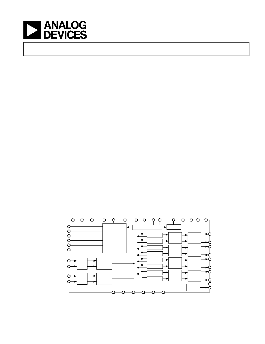
FUNCTIONAL BLOCK DIAGRAM
OUTL1
CONTROL PORT
CLOCK
FILTD
FILTR
ADCLP
ADCLN
ADCRP
ADCRN
DLRCLK
DBCLK
DSDATA1
DSDATA2
DSDATA3
DSDATA4
MCLK
ASDATA
ABCLK
ALRCLK
ODVDD
DVDD
AVDD
AVDD
DVDD
AGND
AGND
AGND
AGND
DGND
DGND
CIN
CLATCH
CCLK
COUT
DIGITAL
FILTER
PD/RST M/S
-
ADC
VOLUME
SERIAL DATA
I/O PORT
DIGITAL
FILTER
-
DAC
V
REF
OUTR1
VOLUME
OUTL2
VOLUME
DIGITAL
FILTER
-
DAC
OUTR2
VOLUME
OUTL3
VOLUME
DIGITAL
FILTER
-
DAC
OUTR3
VOLUME
OUTL4
VOLUME
DIGITAL
FILTER
-
DAC
OUTR4
VOLUME
DIGITAL
FILTER
-
ADC
AD1837
APPLICATIONS
DVD Video and Audio Players
Home Theater Systems
Automotive Audio Systems
Audio/Visual Receivers
Digital Audio Effects Processors
PRODUCT OVERVIEW
The AD1837 is a high performance single-chip codec featuring
four stereo DACs and one stereo ADC. Each DAC comprises a
high performance digital interpolation filter, a multibit -
modulator featuring Analog Devices' patented technology, and
a continuous-time voltage out analog section. Each DAC has
independent volume control and clickless mute functions. The
ADC comprises two 24-bit conversion channels with multibit
- modulators and decimation filters.
The AD1837 also contains an on-chip reference with a nominal
value of 2.25 V.
The AD1837 contains a flexible serial interface that allows for
glueless connection to a variety of DSP chips, AES/EBU receiv-
ers, and sample rate converters. The AD1837 can be configured
in left-justified, right-justified, I
2
S, or DSP compatible serial
modes. Control of the AD1837 is achieved by means of an SPI
compatible serial port. While the AD1837 can be operated from
a single 5 V supply, it also features a separate supply pin for its
digital interface that allows the device to be interfaced to other
devices using 3.3 V power supplies.
The AD1837 is available in a 52-lead MQFP package and is
specified for the industrial temperature range of ≠40∫C to +85∫C.

REV. B
≠2≠
AD1837≠SPECIFICATIONS
TEST CONDITIONS
Supply Voltages (AV
DD
, DV
DD
) 5.0 V
Ambient Temperature
25
C
Input Clock
12.288 MHz, (256
• f
S
Mode)
ADC Input Signal
1.0078125 kHz, ≠1 dBFS (Full Scale)
DAC Input Signal
1.0078125 kHz, 0 dBFS (Full Scale)
Input Sample Rate (f
S
)
48 kHz
Measurement Bandwidth
20 Hz to 20 kHz
Word Width
24 Bits
Load Capacitance
100 pF
Load Impedance
47 k
W
Performance of all channels is identical (exclusive of the Interchannel Gain Mismatch and Interchannel Phase Deviation specifications).
Parameter
Min
Typ
Max
Unit
ANALOG-TO-DIGITAL CONVERTERS
ADC Resolution
24
Bits
Dynamic Range (20 Hz to 20 kHz, ≠60 dB Input)
No Filter
103
dB
A-Weighted
100
105
dB
Total Harmonic Distortion + Noise (THD+N)
≠95
≠88.5
dB
Interchannel Isolation
100
dB
Interchannel Gain Mismatch
0.025
dB
Analog Inputs
Differential Input Range (
± Full Scale)
≠2.828
+2.828
V
Common-Mode Input Voltage
2.25
V
Input Impedance
4
k
W
Input Capacitance
15
pF
V
REF
2.25
V
DC Accuracy
Gain Error
±5
%
Gain Drift
35
ppm/∫C
DIGITAL-TO-ANALOG CONVERTERS
DAC Resolution
Dynamic Range (20 Hz to 20 kHz, ≠60 dBFS Input)
No Filter
103
105
dB
With A-Weighted Filter
105
108
dB
Total Harmonic Distortion + Noise
≠92
dB
Interchannel Isolation
100
dB
DC Accuracy
Gain Error
±4
%
Interchannel Gain Mismatch
0.025
dB
Gain Drift
200
ppm/
C
Interchannel Phase Deviation
±0.1
Degrees
Volume Control Step Size (1023 Linear Steps)
0.098
%
Volume Control Range (Max Attenuation)
60
dB
Mute Attenuation
≠100
dB
De-emphasis Gain Error
±0.1
dB
Full-Scale Output Voltage at Each Pin (Single-Ended)
1.0 (2.8)
V rms (V p-p)
Output Resistance at Each Pin
180
W
Common-Mode Output Voltage
2.25
V
ADC DECIMATION FILTER, 48 kHz
*
Pass Band
21.77
kHz
Pass-Band Ripple
±0.01
dB
Stop Band
26.23
kHz
Stop-Band Attenuation
120
dB
Group Delay
910
ms

REV. B
AD1837
≠3≠
Parameter
Min
Typ
Max
Unit
ADC DECIMATION FILTER, 96 kHz
*
Pass Band
43.54
kHz
Pass-Band Ripple
±0.01
dB
Stop Band
52.46
kHz
Stop-Band Attenuation
120
dB
Group Delay
460
ms
DAC INTERPOLATION FILTER, 48 kHz
*
Pass Band
21.77
kHz
Pass-Band Ripple
±0.06
dB
Stop Band
28.0
kHz
Stop-Band Attenuation
55
dB
Group Delay
340
ms
DAC INTERPOLATION FILTER, 96 kHz
*
Pass Band
43.54
kHz
Pass-Band Ripple
±0.06
dB
Stop Band
52.0
kHz
Stop-Band Attenuation
55
dB
Group Delay
160
ms
DAC INTERPOLATION FILTER, 192 kHz
*
Pass Band
81.2
kHz
Pass-Band Ripple
±0.06
dB
Stop Band
97.0
kHz
Stop-Band Attenuation
80
dB
Group Delay
110
ms
DIGITAL I/O
Input Voltage High
2.4
V
Input Voltage Low
0.8
V
Output Voltage High
ODV
DD
≠ 0.4
V
Output Voltage Low
0.4
V
Leakage Current
±10
mA
POWER SUPPLIES
Supply Voltage (AV
DD
and DV
DD
)
4.5
5.0
5.5
V
Supply Voltage (OV
DD
)
3.0
DV
DD
V
Supply Current I
ANALOG
84
95
mA
Supply Current I
ANALOG
,
Power-Down
55
67
mA
Supply Current I
DIGITAL
64
74
mA
Supply Current I
DIGITAL
,
Power-Down
1
4.5
mA
Dissipation
Operation, Both Supplies
740
mW
Operation, Analog Supply
420
mW
Operation, Digital Supply
320
mW
Power-Down, Both Supplies
280
mW
Power Supply Rejection Ratio
1 kHz, 300 mV p-p Signal at Analog Supply Pins
≠70
dB
20 kHz, 300 mV p-p Signal at Analog Supply Pins
≠75
dB
*Guaranteed by design.
Specifications subject to change without notice.