 | –≠–ª–µ–∫—Ç—Ä–æ–Ω–Ω—ã–π –∫–æ–º–ø–æ–Ω–µ–Ω—Ç: AD1853JRS | –°–∫–∞—á–∞—Ç—å:  PDF PDF  ZIP ZIP |

REV. A
Information furnished by Analog Devices is believed to be accurate and
reliable. However, no responsibility is assumed by Analog Devices for its
use, nor for any infringements of patents or other rights of third parties
which may result from its use. No license is granted by implication or
otherwise under any patent or patent rights of Analog Devices.
a
AD1853*
One Technology Way, P.O. Box 9106, Norwood, MA 02062-9106, U.S.A.
Tel: 781/329-4700
World Wide Web Site: http://www.analog.com
Fax: 781/326-8703
© Analog Devices, Inc., 1999
Stereo, 24-Bit, 192 kHz, Multibit
DAC
FEATURES
5 V Stereo Audio DAC System
Accepts 16-/18-/20-/24-Bit Data
Supports 24 Bits and 192 kHz Sample Rate
Accepts a Wide Range of Sample Rates Including:
32 kHz, 44.1 kHz, 48 kHz, 88.2 kHz, 96 kHz and 192 kHz
Multibit Sigma-Delta Modulator with "Perfect Differential
Linearity Restoration" for Reduced Idle Tones and
Noise Floor
Data Directed Scrambling DAC--Least Sensitive to Jitter
Differential Output for Optimum Performance
120 dB Signal to Noise (Not Muted) at 48 kHz
(A-Weighted Mono)
117 dB Signal to Noise (Not Muted) at 48 kHz
(A-Weighted Stereo)
119 dB Dynamic Range (Not Muted) at 48 kHz Sample
Rate (A-Weighted Mono)
116 dB Dynamic Range (Not Muted) at 48 kHz Sample
Rate (A-Weighted Stereo)
≠107 dB THD+N (Mono Application Circuit, See Figure 30)
≠104 dB THD+N (Stereo)
115 dB Stopband Attenuation (96 kHz)
On-Chip Clickless Volume Control
Hardware and Software Controllable Clickless Mute
Serial (SPI) Control for: Serial Mode, Number of Bits,
Interpolation Factor, Volume, Mute, De-Emphasis, Reset
Digital De-Emphasis Processing for 32, 44.1 and 48 kHz
Sample Rates
Clock Auto-Divide Circuit Supports Five Master-Clock
Frequencies
Flexible Serial Data Port with Right-Justified, Left-
Justified, I
2
S-Compatible and DSP Serial Port Modes
28-Lead SSOP Plastic Package
PRODUCT OVERVIEW
The AD1853 is a complete high performance single-chip stereo
digital audio playback system. It is comprised of a high per-
formance digital interpolation filter, a multibit sigma-delta
modulator, and a continuous-time current-out analog DAC
section. Other features include an on-chip clickless stereo at-
tenuator and mute capability, programmed through an SPI-
compatible serial control port. The AD1853 is fully compatible
with all known DVD formats and supports 48 kHz, 96 kHz and
192 kHz sample rates with up to 24 bits word lengths. It also
provides the "Redbook" standard 50
µs/15 µs digital de-emphasis
filters at sample rates of 32 kHz, 44.1 kHz and 48 kHz.
The AD1853 has a very flexible serial data input port that
allows for glueless interconnection to a variety of ADCs, DSP
chips, AES/EBU receivers and sample rate converters. The
AD1853 can be configured in left-justified, I
2
S, right-justified,
or DSP serial port compatible modes. The AD1853 accepts
serial audio data in MSB first, twos complement format.
The AD1853 operates from a single +5 V power supply. It is
fabricated on a single monolithic integrated circuit and is housed in
a 28-lead SSOP package for operation over the temperature
range 0
∞C to +70∞C.
FUNCTIONAL BLOCK DIAGRAM
SERIAL
DATA
INTERFACE
8
F
S
INTERPOLATOR
SERIAL CONTROL
INTERFACE
AUTO-CLOCK
DIVIDE CIRCUIT
VOLUME
MUTE
CONTROL DATA
INPUT
3
2
DIGITAL
SUPPLY
CLOCK
IN
ANALOG
OUTPUTS
2
2
ZERO
FLAG
ANALOG
SUPPLY
DE-EMPHASIS
MUTE
RESET
2
SERIAL
MODE
DIGITAL
DATA INPUT
AD1853
MULTIBIT SIGMA-
DELTA MODULATOR
ATTEN/
MUTE
IDAC
MULTIBIT SIGMA-
DELTA MODULATOR
8
F
S
INTERPOLATOR
ATTEN/
MUTE
VOLTAGE
REFERENCE
IDAC
INT2
INT4
APPLICATIONS
Hi End: DVD, CD, Home Theater Systems, Automotive
Audio Systems, Sampling Musical Keyboards, Digital
Mixing Consoles, Digital Audio Effects Processors
*Patents Pending.

REV. A
≠2≠
AD1853≠SPECIFICATIONS
TEST CONDITIONS UNLESS OTHERWISE NOTED
Supply Voltages (AV
DD
, DV
DD
)
+5.0 V
Ambient Temperature
+25
∞C
Input Clock
24.576 MHz (512
◊ F
S
Mode)
Input Signal
996.094 kHz
≠0.5 dB Full Scale
Input Sample Rate
48 kHz
Measurement Bandwidth
20 Hz to 20 kHz
Word Width
20 Bits
Input Voltage HI
3.5 V
Input Voltage LO
0.8 V
ANALOG PERFORMANCE (See Figures)
Min
Typ
Max
Units
Resolution
24
Bits
Signal-to-Noise Ratio (20 Hz to 20 kHz)
No Filter (Stereo)
114
dB
No Filter (Mono--See Figure 30)
117
dB
With A-Weighted Filter (Stereo)
117
dB
With A-Weighted Filter (Mono--See Figure 30)
120
dB
Dynamic Range (20 Hz to 20 kHz, ≠60 dB Input)
No Filter (Stereo)
107.5
113
dB
No Filter (Mono--See Figure 30)
116
dB
With A-Weighted Filter (Stereo)
110
116
dB
With A-Weighted Filter (Mono--See Figure 30)
119
dB
Total Harmonic Distortion + Noise (Stereo)
≠94
≠104
dB
0.00063
%
Total Harmonic Distortion + Noise (Mono--See Figure 30)
≠107
dB
0.00045
%
Analog Outputs
Differential Output Range (
±Full Scale w/1 mA into I
REF
)
3.0
mA p-p
Output Capacitance at Each Output Pin
30
pF
Out-of-Band Energy (0.5
◊ F
S
to 75 kHz)
≠90
dB
CMOUT
2.75
V
DC Accuracy
Gain Error
±3.0
%
Interchannel Gain Mismatch
≠0.15
0.01
+0.15
dB
Gain Drift
25
ppm/
∞C
Interchannel Crosstalk (EIAJ Method)
≠125
dB
Interchannel Phase Deviation
±0.1
Degrees
Mute Attenuation
≠100
dB
De-Emphasis Gain Error
±0.1
dB
NOTES
Single-ended current output range: 1 mA
± 0.75 mA.
Performance of right and left channels are identical (exclusive of the Interchannel Gain Mismatch and Interchannel Phase Deviation specifications).
Specifications subject to change without notice.
DIGITAL I/O (+25 C≠AV
DD
, DV
DD
= +5.0 V 10%)
Min
Typ
Max
Units
Input Voltage HI (V
IH
)
2.4
V
Input Voltage LO (V
IL
)
0.8
V
Input Leakage (I
IH
@ V
IH
= 3.5 V)
10
µA
Input Leakage (I
IL
@ V
IL
= 0.8 V)
10
µA
Input Capacitance
20
pF
Output Voltage HI (V
OH
)
DV
DD
≠0.5
DV
DD
≠0.4
V
Output Voltage LO (V
OL
)
0.2
0.5
V
Specifications subject to change without notice.

REV. A
≠3≠
AD1853
POWER
Min
Typ
Max
Units
Supplies
Voltage, Analog and Digital
4.5
5
5.5
V
Analog Current
12
15
mA
Digital Current
28
33
mA
Dissipation
Operation--Both Supplies
200
mW
Operation--Analog Supply
60
mW
Operation--Digital Supply
140
mW
Power Supply Rejection Ratio
1 kHz 300 mV p-p Signal at Analog Supply Pins
≠77
dB
20 kHz 300 mV p-p Signal at Analog Supply Pins
≠72
dB
Specifications subject to change without notice.
TEMPERATURE RANGE
Min
Typ
Max
Units
Specifications Guaranteed
25
∞C
Functionality Guaranteed
0
70
∞C
Storage
≠55
125
∞C
Specifications subject to change without notice.
DIGITAL FILTER CHARACTERISTICS
Sample Rate (kHz)
Passband (kHz)
Stopband (kHz)
Stopband Attenuation (dB)
Passband Ripple (dB)
44.1
DC≠20
24.1≠328.7
110
±0.0002
48
DC≠21.8
26.23≠358.28
110
±0.0002
96
DC≠39.95
56.9≠327.65
115
±0.0005
192
DC≠87.2
117≠327.65
95
+0/≠0.04 (DC≠21.8 kHz)
+0/≠0.5 (DC≠65.4 kHz)
+0/≠1.5 (DC≠87.2 kHz)
Specifications subject to change without notice.
GROUP DELAY
Chip Mode
Group Delay Calculation
F
S
Group Delay
Units
INT8x Mode
5553/(128
◊ F
S
)
48 kHz
903.8
µs
INT4x Mode
5601/(64
◊ F
S
)
96 kHz
911.6
µs
INT2x Mode
5659/(32
◊ F
S
)
192 kHz
921
µs
Specifications subject to change without notice.
DIGITAL TIMING (Guaranteed Over 0 C to +70 C, AV
DD
= DV
DD
= +5.0 V 10%)
Min
Units
t
DMP
MCLK Period (With F
MCLK
= 256
◊ F
LRCLK
)*
54
ns
t
DML
MCLK LO Pulsewidth (All Modes)
0.4
◊ t
DMP
ns
t
DMH
MCLK HI Pulsewidth (All Modes)
0.4
◊ t
DMP
ns
t
DBH
BCLK HI Pulsewidth
20
ns
t
DBL
BCLK LO Pulsewidth
20
ns
t
DBP
BCLK Period
140
ns
t
DLS
LRCLK Setup
20
ns
t
DLH
LRCLK Hold (DSP Serial Port Mode Only)
5
ns
t
DDS
SDATA Setup
5
ns
t
DDH
SDATA Hold
10
ns
t
PDRP
PD/RST LO Pulsewidth
5
ns
*Higher MCLK frequencies are allowable when using the on-chip Master Clock Auto-Divide feature.
Specifications subject to change without notice.
REV. A
AD1853
≠4≠
CAUTION
ESD (electrostatic discharge) sensitive device. Electrostatic charges as high as 4000 V readily
accumulate on the human body and test equipment and can discharge without detection.
Although the AD1853 features proprietary ESD protection circuitry, permanent damage may
occur on devices subjected to high energy electrostatic discharges. Therefore, proper ESD
precautions are recommended to avoid performance degradation or loss of functionality.
WARNING!
ESD SENSITIVE DEVICE
ABSOLUTE MAXIMUM RATINGS*
Min
Max
Units
DV
DD
to DGND
≠0.3
6
V
AV
DD
to AGND
≠0.3
6
V
Digital Inputs
DGND ≠ 0.3
DV
DD
+ 0.3
V
Analog Outputs
AGND ≠ 0.3
AV
DD
+ 0.3
V
AGND to DGND
≠0.3
0.3
V
Reference Voltage
(AV
DD
+ 0.3)/2
Soldering
+300
∞C
10
sec
*Stresses greater than those listed under Absolute Maximum Ratings may cause
permanent damage to the device. This is a stress rating only; functional operation
of the device at these or any other conditions above those indicated in the
operational section of this specification is not implied. Exposure to absolute
maximum rating conditions for extended periods may affect device reliability.
PACKAGE CHARACTERISTICS
Min
Typ
Max
Units
JA
(Thermal Resistance
[Junction-to-Ambient])
109
∞C/W
JC
(Thermal Resistance
[Junction-to-Case])
39
∞C/W
ORDERING GUIDE
Model
Temperature
Package Description
Package Options
AD1853JRS
0
∞C to +70∞C
28-Lead Shrink Small Outline
RS-28
AD1853JRSRL
0
∞C to +70∞C
28-Lead Shrink Small Outline
RS-28 on 13" Reels
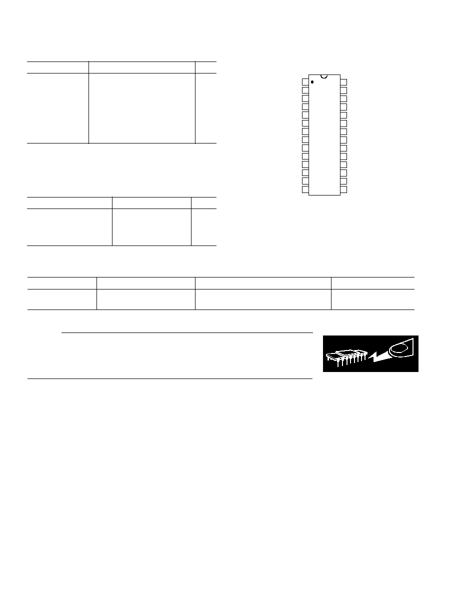
PIN CONFIGURATION
TOP VIEW
(Not to Scale)
28
27
26
25
24
23
22
21
20
19
18
17
16
15
1
2
3
4
5
6
7
8
9
10
11
12
13
14
AD1853
FILTR
OUTL≠
OUTL+
AGND
IREF
DEEMP
ZEROR
DGND
MCLK
CLATCH
CCLK
INT2
INT4
CDATA
FCR
OUTR≠
OUTR+
AVDD
FILTB
IDPM1
IDPM0
DVDD
SDATA
BCLK
L/RCLK
ZEROL
MUTE
RST

REV. A
AD1853
≠5≠
PIN FUNCTION DESCRIPTIONS
Pin
Input/Output
Pin Name
Description
1
I
DGND
Digital Ground.
2
I
MCLK
Master Clock Input. Connect to an external clock source. See Table II for allowable
frequencies.
3
I
CLATCH
Latch input for control data. This input is rising-edge sensitive.
4
I
CCLK
Control clock input for control data. Control input data must be valid on the rising edge
of CCLK. CCLK may be continuous or gated.
5
I
CDATA
Serial control input, MSB first, containing 16 bits of unsigned data. Used for specifying
control information and channel-specific attenuation.
6
I
INT4
◊
Assert HI to select interpolation ratio of 4
◊, for use with double-speed inputs (88 kHz or
96 kHz). Assert LO to select 8
◊ interpolation ratio.
7
I
INT2
◊
Assert HI to select interpolation ratio of 2
◊, for quad-speed inputs (176 kHz or 192 kHz).
Assert LO to select 8
◊ interpolation ratio.
8
O
ZEROR
Right Channel Zero Flag Output. This pin goes HI when Right Channel has no signal
input for more than 1024 LR Clock Cycles.
9
I
DEEMP
De-Emphasis. Digital de-emphasis is enabled when this input signal is HI. This is used to
impose a 50
µs/15 µs response characteristic on the output audio spectrum at an assumed
44.1 kHz sample rate. Curves for 32 kHz and 48 kHz sample rates may be selected via
SPI control register.
10
I
IREF
Connection point for external bias resistor. Voltage held at V
REF
.
11
I
AGND
Analog Ground.
12
O
OUTL+
Left Channel Positive line level analog output.
13
O
OUTL≠
Left Channel Negative line level analog output.
14
O
FILTR
Voltage Reference Filter Capacitor Connection. Bypass and decouple the voltage refer-
ence with parallel 10
µF and 0.1 µF capacitors to the AGND (Pin 11).
15
I
FCR
Filter cap return pin for cap connected to FILTB (Pin 19).
16
O
OUTR≠
Right Channel Negative line level analog output.
17
O
OUTR+
Right Channel Positive line level analog output.
18
I
AVDD
Analog Power Supply. Connect to analog +5 V supply.
19
O
FILTB
Filter Capacitor connection, connect 10
µF capacitor to FCR (Pin 15).
20
I
IDPM1
Input serial data port mode control one. With IDPM0, defines one of four serial modes.
21
I
IDPM0
Input serial data port mode control zero. With IDPM1, defines one of four serial modes.
22
O
ZEROL
Left Channel Zero Flag output. This pin goes HI when Left Channel has no signal input
for more than 1024 LR Clock Cycles.
23
I
MUTE
Mute. Assert HI to mute both stereo analog outputs. Deassert LO for normal operation.
24
I
RST
Reset. The AD1853 is placed in a reset state when this pin is held LO. The AD1853 is
reset on the rising edge of this signal. The serial control port registers are reset to the
default values. Connect HI for normal operation.
25
I
L/RCLK
Left/Right clock input for input data. Must run continuously.
26
I
BCLK
Bit clock input for input data.
27
I
SDATA
Serial input, MSB first, containing two channels of 16/18/20/24 bit twos-complement
data.
28
I
DVDD
Digital Power Supply Connect to digital +5 V supply.

REV. A
AD1853
≠6≠
SDATA
INPUT
LSB
MSB≠2
MSB≠1
LSB+2 LSB+1
MSB≠2
MSB≠1
MSB
LSB+2 LSB+1
LSB
BCLK
INPUT
L/RCLK
INPUT
LEFT CHANNEL
RIGHT CHANNEL
MSB
LSB
Figure 1. Right-Justified Mode
LEFT CHANNEL
RIGHT CHANNEL
MSB≠2
MSB≠1
LSB+2
LSB+1
LSB
MSB≠2
MSB≠1
MSB
LSB+2
LSB+1
LSB
MSB
L/RCLK
INPUT
BCLK
INPUT
SDATA
INPUT
MSB
Figure 2. I
2
S-Justified Mode
MSB≠2
MSB≠1
LSB+2
LSB+1
LSB
MSB≠2
MSB≠1
MSB
LSB+2
LSB+1
LSB
MSB≠1
MSB
L/RCLK
INPUT
BCLK
INPUT
SDATA
INPUT
LEFT CHANNEL
RIGHT CHANNEL
MSB
Figure 3. Left-Justified Mode
SDATA
INPUT
MSB≠1
LSB+2
LSB+1
LSB
MSB≠1
LSB+2
LSB+1
LSB
MSB
MSB≠1
MSB
L/RCLK
INPUT
LEFT CHANNEL
RIGHT CHANNEL
BCLK
INPUT
MSB
Figure 4. Left-Justified DSP Mode
L/RCLK
INPUT
LEFT CHANNEL
RIGHT CHANNEL
BCLK
INPUT
SDATA
INPUT
LSB
MSB≠1
MSB≠2
LSB+2
LSB+1
LSB
MSB
MSB≠1
MSB≠2
LSB+2
LSB+1
LSB
MSB
MSB≠1
MSB
Figure 5. 32
◊ F
S
Packed Mode

REV. A
AD1853
≠7≠
OPERATING FEATURES
Serial Data Input Port
The AD1853's flexible serial data input port accepts data in
twos-complement, MSB-first format. The left channel data field
always precedes the right channel data field. The serial mode is
set by using either the external mode pins (IDPM0 Pin 21 and
IDPM1 Pin 20) or the mode select bits (Bits 4 and 5) in the SPI
control register. To control the serial mode using the external
mode pins, the SPI mode select bits should be set to zero
(default at power-up). To control the serial mode using the SPI
mode select bits, the external mode control pins should be
grounded.
In all modes except for the right-justified mode, the serial port
will accept an arbitrary number of bits up to a limit of 24 (extra
bits will not cause an error, but they will be truncated inter-
nally). In the right-justified mode, control register Bits 8 and 9
are used to set the word length to 16, 20, or 24 bits. The default
on power-up is 24-bit mode. When the SPI Control Port is not
being used, the SPI pins (3, 4 and 5) should be tied LO.
Serial Data Input Mode
The AD1853 uses two multiplexed input pins to control the
mode configuration of the input data port mode.
Table I. Serial Data Input Modes
IDPM1
IDPM0
(Pin 20)
(Pin 21)
Serial Data Input Format
0
0
Right Justified (24 Bits) Default
0
1
I
2
S-Compatible
1
0
Left Justified
1
1
DSP
Figure 1 shows the right-justified mode. LRCLK is HI for the
left channel, LO for the right channel. Data is valid on the rising
edge of BCLK.
In normal operation, there are 64-bit clocks per frame (or 32
per half-frame). When the SPI word length control bits (Bits 8
and 9 in the control register) are set to 24 bits (0:0), the serial
port will begin to accept data starting at the 8th bit clock pulse
after the L/RCLK transition. When the word length control bits
are set to 20-bit mode, data is accepted starting at the 12th bit
clock position. In 16-bit mode, data is accepted starting at the
16th-bit clock position. These delays are independent of the
number of bit clocks per frame, and therefore other data formats
are possible using the delay values described above. For detailed
timing, see Figure 6.
Figure 2 shows the I
2
S mode. L/RCLK is LO for the left chan-
nel, and HI for the right channel. Data is valid on the rising
edge of BCLK. The MSB is left-justified to an L/RCLK transi-
tion but with a single BCLK period delay. The I
2
S mode can be
used to accept any number of bits up to 24.
Figure 3 shows the left-justified mode. L/RCLK is HI for the
left channel, and LO for the right channel. Data is valid on the
rising edge of BCLK. The MSB is left-justified to an L/RCLK
transition, with no MSB delay. The left-justified mode can
accept any word length up to 24 bits.
Figure 4 shows the DSP serial port mode. L/RCLK must pulse
HI for at least one bit clock period before the MSB of the left
channel is valid, and L/RCLK must pulse HI again for at least
one bit clock period before the MSB of the right channel is
valid. Data is valid on the falling edge of BCLK. The DSP serial
port mode can be used with any word length up to 24 bits.
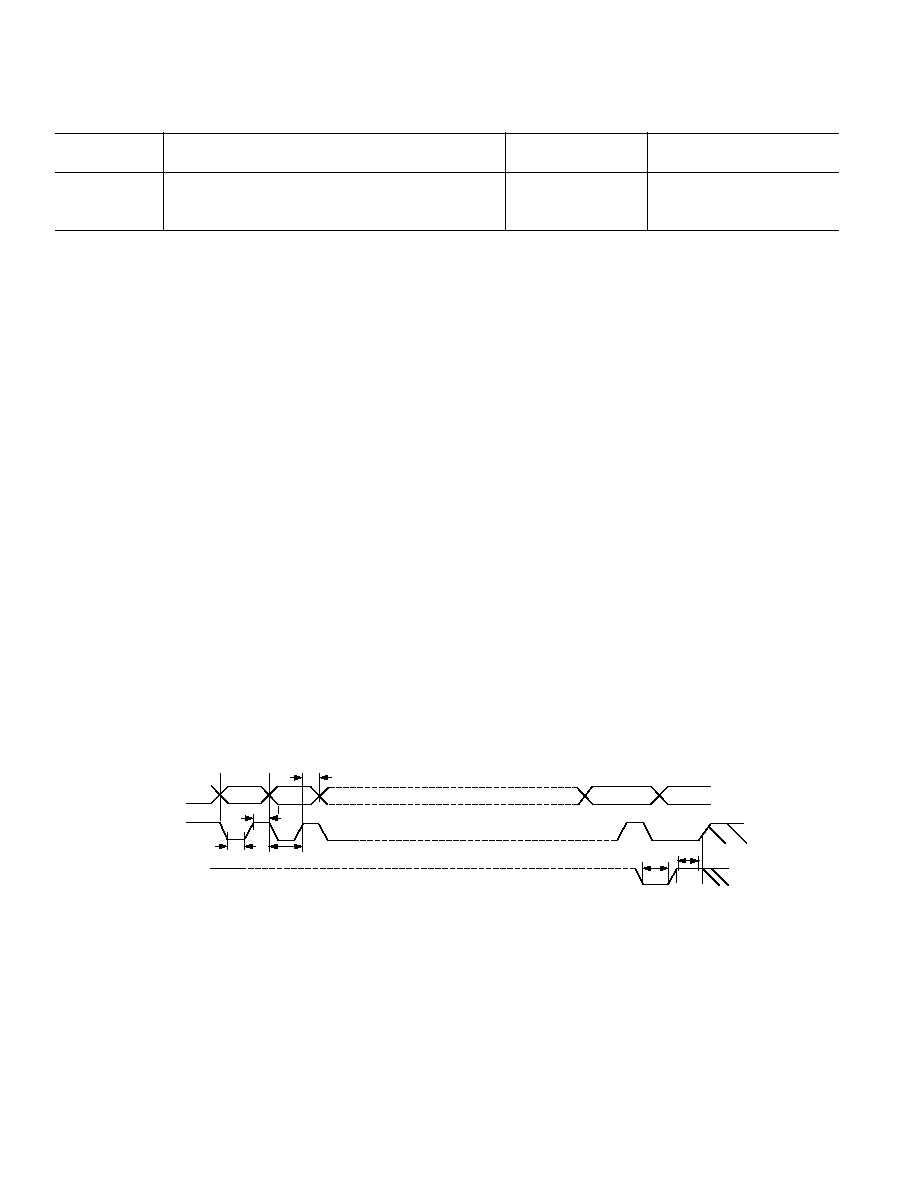
t
DLS
BCLK
L/RCLK
SDATA
LEFT-JUSTIFIED
MODE
SDATA
RIGHT-JUSTIFIED
MODE
LSB
SDATA
I
2
S-JUSTIFIED
MODE
t
DBH
t
DBP
t
DBL
t
DDS
MSB
MSB-1
t
DDH
t
DDS
MSB
t
DDH
t
DDS
t
DDS
t
DDH
t
DDH
MSB
8-BIT CLOCKS
(24-BIT DATA)
12-BIT CLOCKS
(20-BIT DATA)
16-BIT CLOCKS
(16-BIT DATA)
Figure 6. Serial Data Port Timing
REV. A
AD1853
≠8≠
In this mode, it is the responsibility of the DSP to ensure that
the left data is transmitted with the first LRCLK pulse, and that
synchronism is maintained from that point forward.
Note that the AD1853 is capable of a 32
◊ F
S
BCLK frequency
"packed mode" where the MSB is left-justified to an L/RCLK
transition, and the LSB is right-justified to the opposite L/RCLK
transition. L/RCLK is HI for the left channel, and LO for the
right channel. Data is valid on the rising edge of BCLK. Packed
mode can be used when the AD1853 is programmed in right-
justified or left-justified mode. Packed mode is shown is Figure 5.
Master Clock Auto-Divide Feature
The AD1853 has a circuit that autodetects the relationship
between master clock and the incoming serial data, and inter-
nally sets the correct divide ratio to run the interpolator and
modulator. The allowable frequencies for each mode are shown
above.
Serial Control Port
The AD1853 serial control port is SPI-compatible. SPI (Serial
Peripheral Interface) is an industry standard serial port protocol.
The write-only serial control port gives the user access to: select
input mode, soft reset, soft de-emphasis, channel specific at-
tenuation and mute (both channels at once). The SPI port is a
3-wire interface with serial data (CDATA), serial bit clock
(CCLK), and data latch (CLATCH). The data is clocked
into an internal shift register on the rising edge of CCLK.
The serial data should change on the falling edge of CCLK and
be stable on the rising edge of CCLK. The rising edge of
CLATCH is used internally to latch the parallel data from the
serial-to-parallel converter. This rising edge should be aligned
with the falling edge of the last CCLK pulse in the 16-bit frame.
The CCLK can run continuously between transactions.
The serial control data is 16-bit MSB first, and is unsigned. Bits
0 and 1 are used to select 1 of 3 registers (control, volume left,
and volume right). The remaining 14 bits (bits 15:2) are used to
carry the data for the selected register. If a volume register is
selected, then the upper 14 bits are used to multiply the digital
input signal by the control word, which is interpreted as an
unsigned number (for example, 11111111111111 is 0 dB, and
01111111111111 is ≠6 dB, etc.). The default volume control
words on power-up are all 1s (0 dB). The control register only
uses bits 11:2 to carry data; the upper bits (15:12) should al-
ways be written with zeroes, as several test modes are decoded
from these upper bits. The control register defaults on power-up
to 8
◊ interpolation mode, 24-bit right-justified serial mode,
unmuted, and no de-emphasis filter. The intent with these reset
defaults is to enable AD1853 applications without requiring the
use of the serial control port. For those users that do not use the
serial control port, it is still possible to mute the AD1853 output
by using the MUTE pin (Pin 23) signal.
Note that the serial control port timing is asynchronous to the
serial data port timing. Changes made to the attenuator level
will be updated on the next edge of the LRCLK after CLATCH
write pulse as shown in Figure 6.
Table II.
Nominal Input
Internal Sigma-Delta
Chip Mode
Allowable Master Clock Frequencies
Sample Rate
Clock Rate
INT8
◊ Mode
256
◊ F
S
, 384
◊ F
S
, 512
◊ F
S
, 768
◊ F
S
, 1024
◊ F
S
48 kHz
128
◊ F
S
INT4
◊ Mode
128
◊ F
S
, 192
◊ F
S
, 256
◊ F
S
, 384
◊ F
S
, 512
◊ F
S
96 kHz
64
◊ F
S
INT2
◊ Mode
64
◊ F
S
, 96
◊ F
S
, 128
◊ F
S
, 192
◊ F
S
, 256
◊ F
S
192 kHz
32
◊ F
S
D15
D14
D0
t
CHD
t
CCH
t
CSU
t
CCL
t
CLL
t
CLH
CDATA
CCLK
CLATCH
Figure 7. Serial Control Port Timing

REV. A
AD1853
≠9≠
Table III. Digital Timing
Min
Units
t
CCH
CCLK HI Pulsewidth
40
ns
t
CCL
CCLK LOW Pulsewidth
40
ns
t
CSU
CDATA Setup Time
10
ns
t
CHD
CDATA Hold Time
10
ns
t
CLL
CLATCH LOW Pulsewidth
10
ns
t
CLH
CLATCH HI Pulsewidth
10
ns
SPI REGISTER DEFINITIONS
The SPI port allows flexible control of many chip parameters.
It is organized around three registers; a LEFT-CHANNEL
VOLUME register, a RIGHT-CHANNEL VOLUME register
and a CONTROL register. Each WRITE operation to the
AD1853 SPI control port requires 16 bits of serial data in
MSB-first format. The bottom two bits are used to select one
of three registers, and the top 14 bits are then written to that
register. This allows a write to one of the three registers in a
single 16-bit transaction.
The SPI CCLK signal is used to clock in the data. The incom-
ing data should change on the falling edge of this signal. At the
end of the 16 CCLK periods, the CLATCH signal should rise
to latch the data internally into the AD1853.
Register Addresses
The lowest two bits of the 16-bit input word are decoded as
follows to set the register into which the upper 14 bits will be
written.
Bit 1
Bit 0
Register
0
0
Volume Left
1
0
Volume Right
0
1
Control Register
VOLUME LEFT and VOLUME RIGHT Registers
A write operation to the left or right volume registers will acti-
vate the "auto-ramp" clickless volume control feature of the
AD1853. This feature works as follows. The upper 10 bits of
the volume control word will be incremented or decremented by
1 at a rate equal to the input sample rate. The bottom 4 bits are
not fed into the auto-ramp circuit and thus take effect immedi-
ately. This arrangement gives a worst-case ramp time of about
1024/F
S
for step changes of more than 60 dB, which has been
determined by listening tests to be optimal in terms of pre-
venting the perception of a "click" sound on large volume
changes. See Figure 8 for a graphical description of how the
volume changes as a function of time.
The 14-bit volume control word is used to multiply the signal,
and therefore the control characteristic is linear, not dB. A con-
stant dB/step characteristic can be obtained by using a lookup
table in the microprocessor that is writing to the SPI port.
20ms
TIME
≠60
≠60
0
0
LEVEL
≠
dB
VOLUME REQUEST REGISTER
ACTUAL VOLUME REGISTER
Figure 8. Smooth Volume Control

REV. A
AD1853
≠10≠
Control Register
The following table shows the functions of the control register. The control register is addressed by having a "01" in the bottom 2 bits
of the 16-bit SPI word. The top 14 bits are then used for the control register.
Bit 11
Bit 10
Bit 9:8
Bit 7
Bit 6
Bit 5:4
Bit 3:2
INT2
◊ Mode
INT4
◊ Mode
Number of
Soft Reset.
Soft Mute OR'd Serial Mode OR'd
De-Emphasis Filter
OR'd with Pin.
OR'd with Pin.
Bits in Right-
Default = 0
with Pin.
with Mode Pins.
Select.
Default = 0
Default = 0
Justified Serial
Default = 0
IDPMI:IDPM0
0:0 No Filter
Mode.
0:0 Right-Justified
0:1 44.1 kHz Filter
0:0 = 24
0:1 I
2
S
1:0 32 kHz Filter
0:1 = 20
1:0 Left-Justified
1:1 48 kHz Filter
1:0 = 16
1:1 DSP Mode
Default = 0.0
Default = 0:0
Default = 0:0
Mute
The AD1853 offers two methods of muting the analog output.
By asserting the MUTE (Pin 23) signal HI, both the left and
right channel are muted. As an alternative, the user can assert
the mute bit in the serial control register (Bit 6) HI. The AD1853
has been designed to minimize pops and clicks when muting
and unmuting the device by automatically "ramping" the gain
up or down. When the device is unmuted, the volume returns to
the value set in the volume register.
Analog Attenuation
The AD1853 also offers the choice of using IREF (Pin 10) to
attenuate by up to 50 dB in the analog domain. This feature can
be used as an analog volume control. It is also a convenient
place to add a compressor/limiter gain control signal.
Output Drive, Buffering and Loading
The AD1853 analog output stage is able to drive a 1 k
(in
series with 2 nF) load. The analog outputs are usually ac
coupled with a 10
µF capacitor.
De-Emphasis
The AD1853 has a built-in de-emphasis filter that can be used
to decode CDs that have been encoded with the standard
"Redbook" 50
µs/15 µs emphasis response curve. Three curves
are available; one each for 32 kHz, 44.1 kHz and 48 kHz sam-
pling rates. The external "DEEMP" pin (Pin 9) turns on the
44.1 kHz de-emphasis filter. The other filters may be selected
by writing to control Bits 2 and 3 in the control register. If the
SPI port is used to control the de-emphasis filter, the external
DEEMP pin should be tied LO.
Control Signals
The IDPM0 and IDPM1 control inputs are normally con-
nected HI or LO to establish the operating state of the AD1853.
They can be changed dynamically (and asynchronously to
LRCLK and the master clock), but it is possible that a click
or pop sound may result during the transition from one serial
mode to another. If possible, the AD1853 should be placed in
mute before such a change is made.
Figures 9≠14 show the calculated frequency response of the
digital interpolation filters. Figures 15≠27 show the performance
of the AD1853 as measured by an Audio Precision System 2
Cascade. For the wideband plots, the noise floor shown in the
plots is higher than the actual noise floor of the AD1853. This is
caused by the higher noise floor of the "High Bandwidth" ADC
used in the Audio Precision measurement system. The two-tone
test shown in Figure 18 is per the SMPTE standard for measur-
ing Intermodulation Distortion.
FREQUENCY ≠ kHz
0.001
0
dB
2
10
12
14
16
20
0.0008
0.0006
0.0004
0.0002
0
≠0.0002
≠0.0004
≠0.0006
≠0.0008
≠0.001
4
6
8
18
Figure 9. Passband Response 8
◊ Mode, 48 kHz Sample
Rate
FREQUENCY ≠ kHz
0
ATTENUATION
≠
dB
≠60
≠100
≠160
≠20
≠40
≠80
≠120
≠140
0
150
200
50
100
250
300
350
Figure 10. Complete Response, 8
◊ Mode, 48 kHz
Sample Rate

REV. A
AD1853
≠11≠
Typical Performance Characteristics≠
FREQUENCY ≠ kHz
0.5
≠10
dB
5
10
15
20
25
30
35
40
0.4
0.3
0.2
0.1
0
≠0.1
≠0.2
≠0.3
≠0.4
≠0.5
Figure 11. 44 kHz Passband Response 4
◊ Mode, 96 kHz
Sample Rate
FREQUENCY ≠ kHz
2.0
1.5
1.0
0
dB
0
≠0.5
≠1.0
≠2.0
10
20
30
40
50
60
70
80
≠1.5
0.5
Figure 12. 88 kHz Passband Response 2
◊ Mode, 192 kHz
Sample Rate
FREQUENCY ≠ Hz
10
dBr
≠120
100
1k
10k
≠110
≠100
≠90
≠80
≠70
≠60
≠50
Figure 13. THD vs. Frequency Input @ ≠3 dBFS, SR 48 kHz
0
0
dB
150
200
≠60
≠100
50
100
250
≠20
≠40
≠80
≠120
≠140
300
FREQUENCY ≠ kHz
≠160
Figure 14. Complete Response, 4
◊ Mode, 96 kHz
Sample Rate
FREQUENCY ≠ kHz
0
dB
≠60
≠120
≠160
≠40
≠20
≠80
≠100
≠140
0
150
200
50
100
250
Figure 15. Complete Response, 2
◊ Mode, 192 kHz
Sample Rate
dBFS
dB
≠80
≠90
≠100
≠110
≠70
≠60
≠50
≠40
≠30
≠20
≠10
0
≠120
≠100
≠80
≠60
≠40
≠20
0
Figure 16. THD + N Ratio vs. Amplitude Input 1 kHz,
SR 48 kHz, 24-Bit

REV. A
AD1853
≠12≠
FREQUENCY ≠ Hz
10
dBr
≠12
100
1k
10k
≠10
≠8
≠6
≠4
≠2
0
2
Figure 17. Normal De-Emphasis Frequency Response
Input @ ≠10 dBFS, SR 48 kHz
FREQUENCY ≠ kHz
dBr
≠90
≠110
≠130
≠150
≠70
≠50
≠30
≠10
0
2
4
6
8
10
12
14
16
18
20
22
Figure 18. SMPTE/DIN 4:1 IMD 60 Hz/7 kHz @ 0 dBFS
dBFS
dBr
≠80
≠100
≠120
≠140
≠60
≠40
≠20
0
≠140
≠120
≠100
≠60
≠40
≠20
0
≠80
Figure 19. Linearity vs. Amplitude Input 200 Hz,
SR 48 kHz, 24-Bit Word
FREQUENCY ≠ kHz
dBr
≠130
≠140
≠150
≠120
≠110
≠100
≠90
0
2
4
6
8
10
12
14
16
18
20
22
≠80
≠70
≠60
≠50
≠40
≠30
≠20
≠10
0
Figure 21. Input 0 dBFS @ 1 kHz, BW 10 Hz to 22 kHz,
SR 48 kHz, THD+N 104 dBFS
FREQUENCY ≠ kHz
dBr
≠130
≠140
≠150
≠120
≠110
≠100
≠90
0
2
4
6
8
10
12
14
16
18
20
22
≠80
≠70
≠60
≠50
≠160
Figure 22. Dynamic Range for 1 kHz @ ≠60 dBFS,
116 dB, Triangular Dithered Input
FREQUENCY ≠ kHz
dBr
≠130
≠140
≠150
≠160
≠120
≠110
≠100
≠90
0
2
4
6
8
10
12
14
16
18
20
22
Figure 20. Noise Floor for Zero Input, SR 48 kHz,
SNR ≠117 dBFS A-Weighted

REV. A
AD1853
≠13≠
FREQUENCY ≠ Hz
10
dBr
≠100
≠90
≠60
100
1k
10k
≠70
≠80
Figure 23. Power Supply Rejection vs. Frequency
AV
DD
5 V dc + 100 mV p-p ac
FREQUENCY ≠ kHz
0
≠100
120
20
dBr
40
60
80
100
≠10
≠40
≠70
≠80
≠90
≠20
≠30
≠50
≠60
≠110
≠120
≠130
≠140
Figure 24. Wideband Plot, 15 kHz Input, 8
◊ Interpolation,
SR 48 kHz
FREQUENCY ≠ kHz
0
≠100
120
20
dBr
40
60
80
100
≠10
≠40
≠70
≠80
≠90
≠20
≠30
≠50
≠60
≠110
≠120
≠130
≠140
Figure 25. Wideband Plot, 37 kHz Input, 4
◊ Interpolation,
SR 96 kHz
FREQUENCY ≠ kHz
0
≠100
30
5
dBr
10 15 20 25
≠10
≠40
≠70
≠80
≠90
≠20
≠30
≠50
≠60
≠110
≠120
≠130
≠140
≠150
≠160
35 40 45 50 55 60 65 70 75 80
Figure 26. Wideband Plot, 25 kHz Input, 2
◊ Interpolation,
SR 192 kHz
FREQUENCY ≠ kHz
0
≠100
30
5
dBr
10 15 20 25
≠10
≠40
≠70
≠80
≠90
≠20
≠30
≠50
≠60
≠110
≠120
≠130
≠140
≠150
≠160
35 40 45 50 55 60 65 70 75 80
Figure 27. Wideband Plot, 75 kHz Input, 2
◊ Interpolation,
SR 192 kHz

REV. A
AD1853
≠14≠
STEREO MODE OUTPUT FILTER
HDR3 F
N
1
2
44/48
0
0
96
1
0
192
0
1
NO
1
1
C37
47pF
C11
100nF
DVDD
C24
47nF
R4
1k
DVDD AVDD
OUTR+
OUTR≠
OUTL+
OUTL≠
FILTB
DGND
AGND
FCR
U5
AD1853JRS
C26
10 F
C56
100nF
SIGNAL
SOURCE
J1
R3
750
R1
75
R8
10k
R7
10k
R9
10k
C9
100nF
DVDD
C8
100nF
AVDD
DVDD
DS1
ZERO
LEFT
C10
100nF
FB3
600Z
NOTE:
= DGND
= AGND
INT4
INT2
SDATA
L/RCLK
BCLK
MCLK
IDPM0
IDPM1
DEEMP
MUTE
CLATCH
CCLK
CDATA
ZEROR
ZEROL
RST
FILTR
IREF
CLATCH
CCLK
CDATA
ZR
ZL
RST
+
≠
R28
2.67k
AGND
DGND
SAMPLE RATE
MODE
R5
10k
R6
10k
DVDD
R19
10k
CLK/I0
I1
I 2
I 3
I 4
I 5
I 6
I 7
I 8
I 9
I10
I11
I /O9
I / O 8
I /O7
I /O6
I /O5
I /O4
I /O3
I /O2
I / O 1
I/O 0
U4
PALCE22V10-J
MCLK
EXT MCLK
EXT SCLK
EXT L/RCLK
EXT SDATA
HDR3
R18
10k
3
8
IDPM1
DVDD
R17
10k
2
9
IDPM0
DVDD
S2B
S2C
VREF
R23
274
Q1
2N2222
DS4
DVDD
VERF
PREEMPH
1
2
3
DVDD
U3A
74HC00D
C5
100nF
DVDD
C6
100nF
SDATA
FSYNC
SCK
MCK
M0
M1
M2
M3
C
U
CBL
VERF
ERF
C0/E0
Ca/E1
Cb/E2
Cc/F0
Cd/F1
Ce/F2
SEL
CSI2/FCK
DGND
AGND
VA+
VD+
FB2
600Z
R24
100
R12
10k
C35
47pF
R25
100
R13
10k
C36
47pF
R26
100
R14
10k
C34
47pF
R27
100
R15
10k
EXT SDATA
EXT L/RCLK
EXT SCLK
EXT MCLK
DVDD
R11
10k
1
10
DVDD
S2A
SPDIF/EXT
SPDIF/EXT
I/F
SELECT
ROUT+
ROUT≠
LOUT+
LOUT≠
V
REF
+2.7V
HDR2
EXT I/F
IN
F
S
64F
S
256F
S
U2
CS8414-CS
12
13
11
U3D
74HC00D
SET Ib = 1mA
DS2
ZERO
RIGHT
R21
274
9
10
8
U3C
74HC00D
DS3
DEEMPH
R22
274
4
5
6
U3B
74HC00D
DVDD
R20
274
DVDD
C12
100nF
ZR
ZL
FILT
C1
10nF
S1
C2
10nF
RXP
RXN
1
0
SPNIF
IN
DGND
SHLD DGND
U1
TORX173
OUT
DVDD
TOSLINK
IN
C4
100nF
R2
3.40k
500mVp-p
FB1
600Z
DVDD
R10
10k
MUTE
R16
10k
4
7
DEEMPH
DVDD
S2D
ON
OFF
DEEMPH
5
6
MUTE
S2E
OFF
ON
CDATA
CCLK
CLATCH
MCLK
DVDD
HDR1
EXT C
I/F
1
2
3
4
5
1
0
U2 DATA SOURCE
I
2
S SERIAL
DATA MODE
DEEMPH OFF
MUTE OFF
S2A
S2B
S2C
S2D
S2E
#98107-02-3 REV. 1.1
1
1
Figure 28. Digital Receiver, MUX and AD1853 DAC

REV. A
AD1853
≠15≠
U8B
OP275
C38
220pF
NP0
R29
2.94k
R41
604
R34
2.74k
C43
680pF
NP0
R33
2.74k
C42
680pF
NP0
R30
2.94k
R35
2.74k
R36
2.74k
C39
220pF
NP0
C50
2.2nF
NP0
RIGHT
OUT
J2
1
GAUSSIAN FILTER RESPONSE
≠3dB CORNER FREQUENCY: 75kHz
OUTPUT BUFFERS AND LP FILTERS
0
R43
49.9k
C46
330pF, NP0
C52*
NP
C21
100nF
≠AV
SS
C23
100nF
+AV
CC
OP275
U6A
R48
4.12k
U6B
OP275
C53*
NP
C47
330pF, NP0
R49
4.12k
C57
220pF
NP0
+
≠
C7
100nF
U8A
OP275
C40
220pF
NP0
R31
2.94k
R42
604
R38
2.74k
C45
680pF
NP0
R37
2.74k
C44
680pF
NP0
R32
2.94k
R39
2.74k
R40
2.74k
C41
220pF
NP0
C51
2.2nF
NP0
LEFT
OUT
J3
1
0
R44
49.9k
C48
330pF, NP0
C54*
NP
C20
100nF
≠AV
EE
C22
100nF
+AV
CC
OP275
U7A
R50
4.12k
U7B
OP275
C55*
NP
C49
330pF, NP0
R51
4.12k
C58
220pF
NP0
C19
100nF
≠AV
SS
C18
100nF
+AV
CC
R52
402
R53
402
C25
10 F
ROUT+
LOUT+
LOUT≠
V
REF
+2.7V
AVDD
AGND
+15V dc
DS5
POWER
FB4
600Z
IN
IN
ERR
SD
OUT
OUT
NR
GND
+AV
CC
J6
U11
ADP3303-5.0
C3
10nF
C16
100nF
+
≠
C31
10 F
+
≠
C30
10 F
C15
100nF
+
≠
C32
10 F
+5V REG
R47
332
≠AV
SS
CR2
1SMB15AT3
0V
AGND
J7
+
≠
C33
10 F
≠15V dc
J8
VOLTAGE REGULATORS AND SUPPLY FILTERING
DVDD
+9V dc
TO
+15V dc
FB5
600Z
J4
U9
LM317
+
≠
C29
10 F
+
≠
V
IN
R46
715
CR1
1SMB15AT3
0V
DGND
J5
+
≠
C28
10 F
V
OUT
GND
R45
243
+5V REG
DGND
C13
100nF
C27
10 F
CR3
1N4001
C14
100nF
DVDD
PFI
MR
V
CC
RESET
RESET
PFO
GND
RST
U10
ADM707AR
S3
RESET
C17
100nF
RESET GENERATOR
NOTE:
= DGND
= AGND
*NOT POPULATED
ROUT≠
Figure 29. DAC Output LP Filter, Power and Reset

REV. A
AD1853
≠16≠
C3503a
≠
8
≠
4/99
PRINTED IN U.S.A.
U1
AD797
C1
220pF
NP0
R1
2.94k
R7
604
R4
2.74k
C4
680pF
NP0
R3
2.74k
C3
680pF
NP0
R2
2.94k
R5
2.74k
R6
2.74k
C2
220pF
NP0
C5
2.2nF
NP0
GAUSSIAN FILTER RESPONSE
≠3dB CORNER FREQUENCY: 75kHz
I/V CONVERTERS AND LP FILTER
R8
49.9k
C6
68pF, NP0
AD797
U2
R9*
2.87k
U3
C7
68pF, NP0
R10*
2.87k
+
≠
C8
100nF
R12
100
PIN 13
LOUT≠
PIN 12
LOUT+
V
REF
+2.78V
R11
100
AD797
OUT
6Vrms
J1
1
0
PIN 16
ROUT≠
PIN 17
ROUT+
NOTES:
1. R9, R10 MUST BE LOW NOISE TYPES.
METAL FILM IS RECOMMENDED.
2. RIGHT CHANNEL DIGITAL DATA MUST BE INVERTED.
C15
10 F
TANT
+AV
CC
≠AV
SS
J2
+
≠
C14
100nF
0V
AGND
J4
+
≠
C17
10 F
TANT
J3
C13
100nF
C16
10 F
TANT
C12
100nF
C11
100nF
C10
100nF
C9
100nF
+16.5V dc
≠16.5V dc
NOTE:
= AGND
Figure 30. Mono Application Circuit
OUTLINE DIMENSIONS
Dimensions shown in inches and (mm).
28-Lead Shrink Small Outline Package (SSOP)
(RS-28)
0.009 (0.229)
0.005 (0.127)
0.03 (0.762)
0.022 (0.558)
8∞
0∞
0.008 (0.203)
0.002 (0.050)
0.07 (1.79)
0.066 (1.67)
0.078 (1.98)
0.068 (1.73)
0.015 (0.38)
0.010 (0.25)
SEATING
PLANE
0.0256
(0.65)
BSC
0.311 (7.9)
0.301 (7.64)
0.212 (5.38)
0.205 (5.21)
28
15
14
1
0.407 (10.34)
0.397 (10.08)
PIN 1