 | ÐлекÑÑоннÑй компоненÑ: AD1854J/K | СкаÑаÑÑ:  PDF PDF  ZIP ZIP |
AD1854 Data Sheet
a
AD1854
Information furnished by Analog Devices is believed to be accurate and
reliable. However, no responsibility is assumed by Analog Devices for its
use, nor for any infringements of patents or other rights of third parties
which may result from its use. No license is granted by implication or
otherwise under any patent or patent rights of Analog Devices.
REV. A
One Technology Way, P.O. Box 9106, Norwood, MA 02062-9106, U.S.A.
Tel: 781/329-4700
World Wide Web Site: http://www.analog.com
Fax: 781/326-8703
© Analog Devices, Inc., 2000
Stereo, 96 kHz, Multibit
DAC
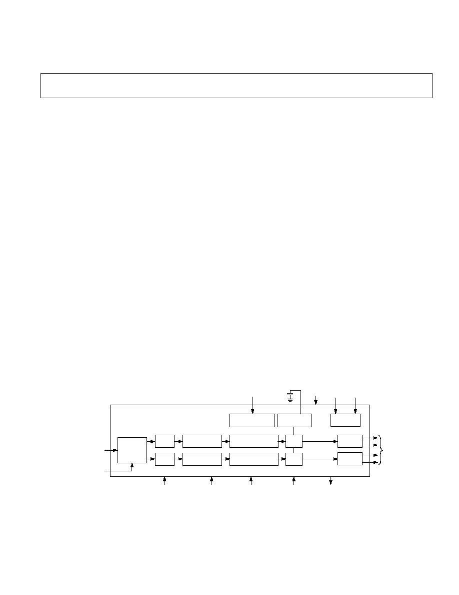
FUNCTIONAL BLOCK DIAGRAM
ATTEN/
MUTE
ATTEN/
MUTE
SERIAL
DATA
INTERFACE
8
F
S
INTERPOLATOR
MULTIBIT SIGMA-
DELTA MODULATOR
SERIAL CONTROL
INTERFACE
CLOCK
CIRCUIT
OUTPUT
BUFFER
OUTPUT
BUFFER
DAC
DAC
MULTIBIT SIGMA-
DELTA MODULATOR
VOLTAGE
REFERENCE
VOLUME
MUTE
CONTROL DATA
INPUT
3
2
DIGITAL
SUPPLY
CLOCK
IN
96/
48F
S
CLOCK
ANALOG
OUTPUTS
2
2
ZERO
FLAG
ANALOG
SUPPLY
DE-EMPHASIS
MUTE
PD/RST
2
SERIAL
MODE
16-/18-/20-/24-BIT
DIGITAL
DATA INPUT
AD1854
8
F
S
INTERPOLATOR
FEATURES
5 V Stereo Audio DAC System
Accepts 16-/18-/20-/24-Bit Data
Supports 24 Bits and 96 kHz Sample Rate
Multibit Sigma-Delta Modulator with "Perfect Differential
Linearity Restoration" for Reduced Idle Tones and
Noise Floor
Data Directed Scrambling DAC--Least Sensitive to Jitter
Differential Output for Optimum Performance
113 dB Dynamic
Range at 48 kHz Sample Rate
(AD1854KRS)
112 dB Signal-to-Noise at 48 kHz Sample Rate
(AD1854KRS)
101 THD+N (AD1854KRS)
On-Chip Volume Control with 1024 Steps
Hardware and Software Controllable Clickless Mute
Zero Input Flag Outputs for Left and Right Channels
Digital De-Emphasis Processing
Supports 256 F
S
or 384 F
S
Master Mode Clock
Switchable Clock Doubler
Power-Down Mode Plus Soft Power-Down Mode
Flexible Serial Data Port with Right-Justified, Left-
Justified, and I
2
S-Compatible
28-Lead SSOP Plastic Package
APPLICATIONS
DVD, CD, Set-Top Boxes, Home Theater Systems,
Automotive Audio Systems, Sampling Musical
Keyboards, Digital Mixing Consoles, Digital Audio
Effects Processors
PRODUCT OVERVIEW
The AD1854 is a high performance, single-chip stereo, audio
DAC delivering 113 dB Dynamic Range and 112 dB SNR
(A-weighted--not muted) at 48 kHz sample rate. It is comprised
of a multibit sigma-delta modulator with dither, continuous
time analog filters and analog output drive circuitry. Other features
include an on-chip stereo attenuator and mute, programmed
through an SPI-compatible serial control port. The AD1854
is fully compatible with current DVD formats, including 96 kHz
sample frequency and 24 bits. It is also backwards compatible
by supporting 50
µs/15 µs digital de-emphasis intended for
"redbook" 44.1 kHz sample frequency playback from com-
pact discs.
The AD1854 has a very simple but very flexible serial data input
port that allows for glueless interconnection to a variety of ADCs,
DSP chips, AES/EBU receivers and sample rate converters.
The AD1854 can be configured in left-justified, I
2
S, and right-
justified. The AD1854 accepts serial audio data in MSB first,
twos-complement format. A power-down mode is offered to mini-
mize power consumption when the device is inactive. The AD1854
operates from a single 5 V power supply. It is fabricated on a single
monolithic integrated circuit and housed in a 28-lead SSOP
package for operation over the temperature range 0
°C to 70°C.

2
REV. A
AD1854SPECIFICATIONS
TEST CONDITIONS UNLESS OTHERWISE NOTED
Supply Voltages (AV
DD
, DV
DD
)
5.0 V
Ambient Temperature
25
°C
Input Clock
12.288 MHz (256
× F
S
Mode)
Input Signal
1.0013 kHz
0.5 dB Full Scale
Input Sample Rate
48 kHz
Measurement Bandwidth
20 Hz to 20 kHz
Word Width
20 Bits
Load Capacitance
100 pF
Load Impedance
47 k
Input Voltage HI
2.4 V
Input Voltage LO
0.8 V
Performance of right and left channels are identical (exclusive of the Interchannel Gain Mismatch and Interchannel Phase Deviation specifications).
ANALOG PERFORMANCE
Min
Typ
Max
Unit
Resolution
20
Bits
Signal-to-Noise Ratio (20 Hz to 20 kHz)
No Filter (AD1854JRS)
105
dB
No Filter (AD1854KRS)
110
dB
With A-Weighted Filter (AD1854JRS)
108
dB
With A-Weighted Filter (AD1854KRS)
112
dB
Dynamic Range (20 Hz to 20 kHz, 60 dB Input)
No Filter (AD1854JRS)
105
dB
No Filter (AD1854KRS)
106
110
dB
With A-Weighted Filter (AD1854JRS)
108
dB
With A-Weighted Filter (AD1854KRS)
108
113
dB
Total Harmonic Distortion + Noise (AD1854JRS) V
O
= 0 dB
88
97
dB
Total Harmonic Distortion + Noise (AD1854KRS) V
O
= 0 dB
94
101
dB
Total Harmonic Distortion + Noise (AD1854JRS and
89
dB
AD1854KRS) V
O
= 20 dB
Total Harmonic Distortion + Noise (AD1854JRS and
49
dB
AD1854KRS) V
O
= 60 dB
Analog Outputs
Differential Output Range (
±Full Scale)
5.6
V p-p
Output Impedance at Each Output Pin
<200
Output Capacitance at Each Output Pin
20
pF
Out-of-Band Energy (0.5
× F
S
to 100 kHz)
72.5
dB
CMOUT
2.25
V
DC Accuracy
Gain Error
11.0
±3.0
+11.0
%
Interchannel Gain Mismatch
0.15
+0.15
dB
Gain Drift
200
300
ppm/
°C
Interchannel Crosstalk (EIAJ Method)
120
dB
Interchannel Phase Deviation
±0.1
Degrees
Mute Attenuation
100
dB
De-Emphasis Gain Error
±0.1
dB
DIGITAL I/O (0 C to 70 C)
Min
Typ
Max
Unit
Input Voltage HI (V
IH
)
2.2
V
Input Voltage LO (V
IL
)
0.8
V
High Level Output Voltage (V
OH
) I
OH
= 1 mA
2.0
V
Low Level Output Voltage (V
OL
) I
OL
= 1 mA
0.4
V
Input Leakage (I
IH
@ V
IH
= 2.4 V)
10
µA
Input Leakage (I
IL
@ V
IL
= 0.8 V)
10
µA
Input Capacitance
20
pF
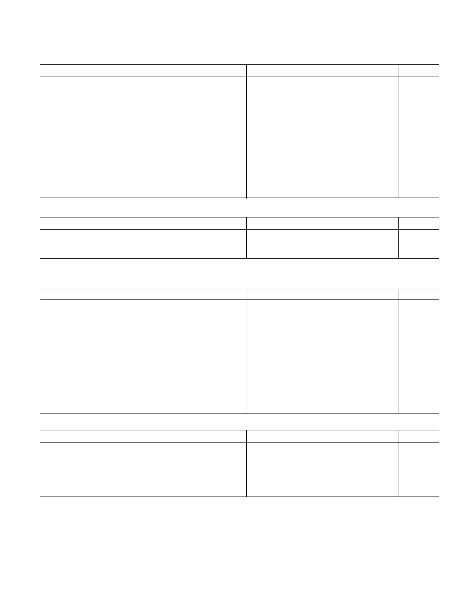
3
REV. A
AD1854
POWER
Min
Typ
Max
Unit
Supplies
Voltage, Analog and Digital
4.5
5
5.5
V
Analog Current
26
30
35
mA
Analog Current--Power-Down
26
29
33.5
mA
Digital Current
14
17
20
mA
Digital Current--Power-Down
1.5
2.5
5.5
mA
Dissipation
Operation--Both Supplies
250
mW
Operation--Analog Supply
150
mW
Operation--Digital Supply
100
mW
Power-Down--Both Supplies
190
mW
Power Supply Rejection Ratio
1 kHz 300 mV p-p Signal at Analog Supply Pins
60
dB
20 kHz 300 mV p-p Signal at Analog Supply Pins
50
dB
TEMPERATURE RANGE
Min
Typ
Max
Unit
Specifications Guaranteed
25
°C
Functionality Guaranteed
0
70
°C
Storage
55
+125
°C
DIGITAL TIMING (Guaranteed over 0 C to 70 C, AV
DD
= DV
DD
= 5.0 V 10%)
Min
Max
Unit
t
DMP
MCLK Period (512 F
S
Mode)
35
ns
t
DMP
MCLK Period (384 F
S
Mode)
48
ns
t
DMP
MCLK Period (256 F
S
Mode)
70
ns
t
DML
MCLK LO Pulsewidth (All Mode)
0.4
× t
DMP
ns
t
DMH
MCLK HI Pulsewidth (All Mode)
0.4
× t
DMP
ns
t
DBH
BCLK HI Pulsewidth
20
ns
t
DBL
BCLK LO Pulsewidth
20
ns
t
DBP
BCLK Period
140
ns
t
DLS
L/RCLK Setup
20
ns
t
DLH
L/RCLK Hold (DSP Serial Port Mode Only)
5
ns
t
DDS
SDATA Setup
5
ns
t
DDH
SDATA Hold
10
ns
t
PDRP
PD/RST LO Pulsewidth
4 MCLK Periods
ns
DIGITAL FILTER CHARACTERISTICS
Min
Typ
Max
Unit
Passband Ripple
±0.04
dB
Stopband
Attenuation
47
dB
Passband
0.448
F
S
Stopband
0.552
F
S
Group Delay
106/F
S
sec
Group Delay Variation
0
µs
Specifications subject to change without notice.
4
AD1854
REV. A
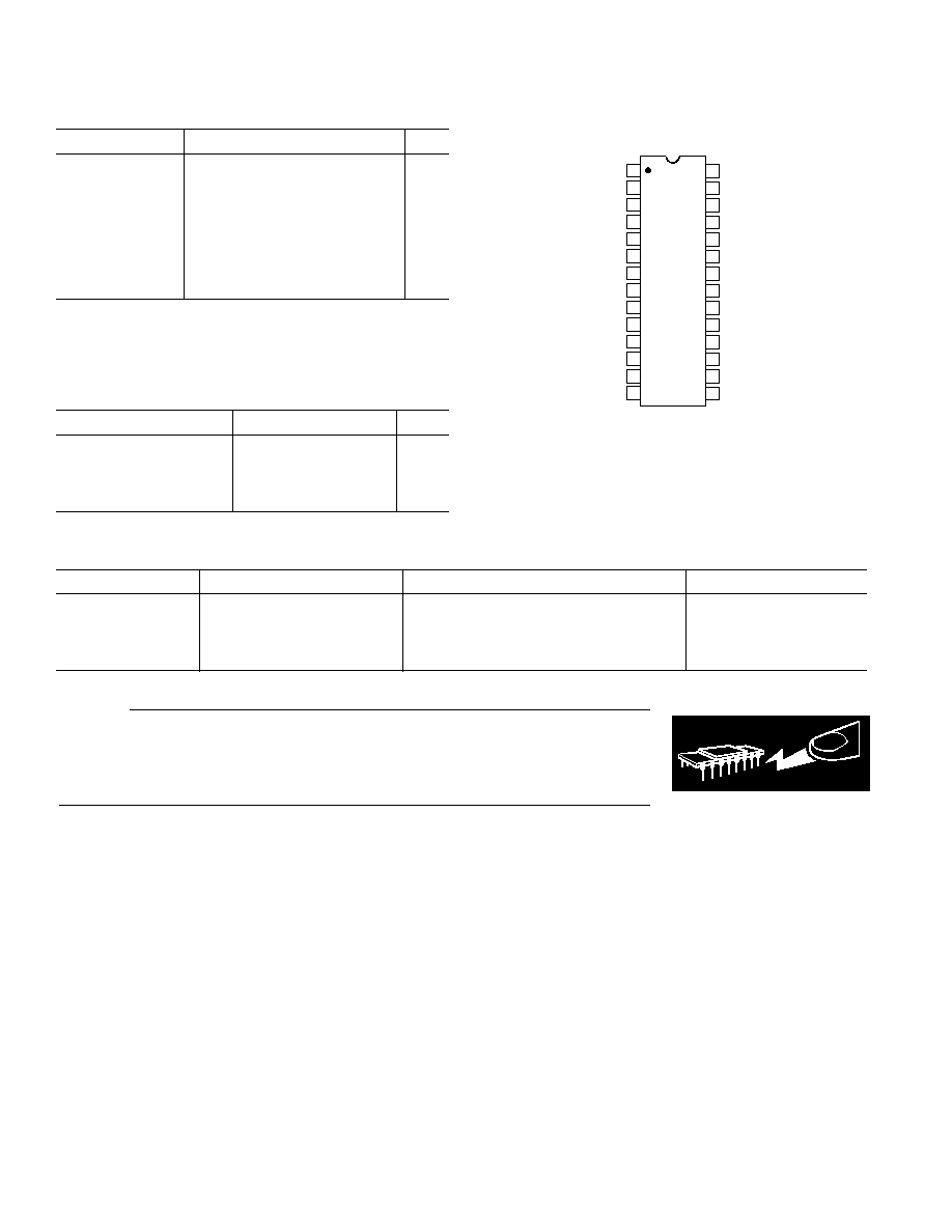
CAUTION
ESD (electrostatic discharge) sensitive device. Electrostatic charges as high as 4000 V readily
accumulate on the human body and test equipment and can discharge without detection.
Although the AD1854 features proprietary ESD protection circuitry, permanent damage may
occur on devices subjected to high-energy electrostatic discharges. Therefore, proper ESD
precautions are recommended to avoid performance degradation or loss of functionality.
WARNING!
ESD SENSITIVE DEVICE
ABSOLUTE MAXIMUM RATINGS
*
Min
Max
Unit
DV
DD
to DGND
0.3
+6
V
AV
DD
to AGND
0.3
+6
V
Digital Inputs
DGND 0.3
DV
DD
+ 0.3
V
Analog Outputs
AGND 0.3
AV
DD
+ 0.3
V
AGND to DGND
0.3
+0.3
V
Reference Voltage
(AV
DD
+ 0.3)/2
Soldering
300
°C
10
sec
*Stresses greater than those listed under Absolute Maximum Ratings may cause
permanent damage to the device. This is a stress rating only; functional operation
of the device at these or any other conditions above those indicated in the
operational section of this specification is not implied. Exposure to absolute
maximum rating conditions for extended periods may affect device reliability.
PACKAGE CHARACTERISTICS
Min
Typ
Max
Unit
JA
(Thermal Resistance
109
°C/W
[Junction-to-Ambient])
JC
(Thermal Resistance
39
°C/W
[Junction-to-Case])
ORDERING GUIDE
Model
Temperature
Package Description
Package Option
AD1854JRS
0
°C to 70°C
28-Lead Shrink Small Outline
RS-28
AD1854JRSRL
0
°C to 70°C
28-Lead Shrink Small Outline
RS-28 on 13" Reels
AD1854KRS
0
°C to 70°C
28-Lead Shrink Small Outline
RS-28
AD1854KRSRL
0
°C to 70°C
28-Lead Shrink Small Outline
RS-28 on 13" Reels
PIN CONFIGURATION
TOP VIEW
(Not to Scale)
28
27
26
25
24
23
22
21
20
19
18
17
16
15
1
2
3
4
5
6
7
8
9
10
11
12
13
14
AD1854
FILTR
OUTR
OUTR+
AGND
96/
48
DEEMP
ZEROR
DGND
MCLK
CLATCH
CCLK
X2MCLK
384/
256
CDATA
AGND
OUTL
OUTL+
AVDD
FILTB
IDPM1
IDPM0
DVDD
SDATA
BCLK
L/
RCLK
ZEROL
MUTE
PD/RST
AD1854
5
REV. A
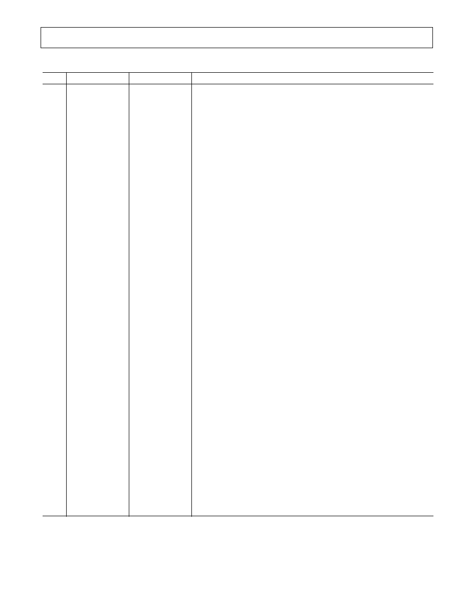
PIN FUNCTION DESCRIPTIONS
Pin
Input/Output
Pin Name
Description
1
I
DGND
Digital Ground.
2
I
MCLK
Master Clock Input. Connect to an external clock source at either 256, 384
or 512 F
S
.
3
I
CLATCH
Latch input for control data. This input is rising-edge sensitive.
4
I
CCLK
Control clock input for control data. Control input data must be valid on the
rising edge of CCLK. CCLK may be continuous or gated.
5
I
CDATA
Serial control input, MSB first, containing 16 bits of unsigned data per
channel. Used for specifying channel-specific attenuation and mute.
6
I
384/256
Selects the master clock mode as either 384 times the intended sample
frequency (HI) or 256 times the intended sample frequency (LO). The state
of this input should be hardwired to logic HI or logic LO, or may be changed
while the AD1854 is in power-down/reset. It must not be changed while the
AD1854 is operational.
7
I
X2MCLK
Selects internal clock doubler (LO) or internal clock = MCLK (HI).
8
O
ZEROR
Right Channel Zero Flag Output. This pin goes HI when Right Channel has
no signal input for more than 1024 LR Clock Cycles.
9
I
DEEMP
De-Emphasis. Digital de-emphasis is enabled when this input signal is HI.
This is used to impose a 50
µs/15 µs response characteristic on the output
audio spectrum at an assumed 44.1 kHz sample rate.
10
I
96/48
Selects 48 kHz (LO) or 96 kHz Sample Frequency Control.
11, 15
I
AGND
Analog Ground.
12
O
OUTR+
Right Channel Positive line level analog output.
13
O
OUTR
Right Channel Negative line level analog output.
14
O
FILTR
Voltage Reference Filter Capacitor Connection. Bypass and decouple the
voltage reference with parallel 10
µF and 0.1 µF capacitors to the AGND.
16
O
OUTL
Left Channel Negative line level analog output.
17
O
OUTL+
Left Channel Positive line level analog output.
18
I
AVDD
Analog Power Supply. Connect to analog 5 V supply.
19
O
FILTB
Filter Capacitor connection, connect 10
µF capacitor to AGND.
20
I
IDPM1
Input serial data port mode control one. With IDPM0, defines one of four
serial modes.
21
I
IDPM0
Input serial data port mode control zero. With IDPM1, defines one of four
serial modes.
22
O
ZEROL
Left Channel Zero Flag Output. This pin goes HI when Left Channel has no
signal input for more than 1024 LR Clock Cycles.
23
I
MUTE
Mute. Assert HI to mute both stereo analog outputs. Deassert LO for nor-
mal operation.
24
I
PD/RST
Power-Down/Reset. The AD1854 is placed in a low power consumption
mode when this pin is held LO. The AD1854 is reset on the rising edge of
this signal. The serial control port registers are reset to the default values.
Connect HI for normal operation.
25
I
L/RCLK
Left/Right clock input for input data. Must run continuously.
26
I
BCLK
Bit clock input for input data. Need not run continuously; may be gated or
used in a burst fashion.
27
I
SDATA
Serial input, MSB first, containing two channels of 16, 18, 20, and 24 bits of
twos complement data per channel.
28
I
DVDD
Digital Power Supply Connect to digital 5 V supply.
6
AD1854
REV. A
OPERATING FEATURES
Serial Data Input Port
The AD1854's flexible serial data input port accepts data in
twos-complement, MSB-first format. The left channel data field
always precedes the right channel data field. The input data
consists of either 16, 18, 20, or 24 bits, as established by the
mode select pins (IDPM0 Pin 21 and IDPM1 Pin 20) or the
mode select bits (Bits 15 and 14) in the control register through
the SPI (Serial Peripheral Interface) control port. Neither the
pins nor the SPI controls has preference; to ensure proper control,
the selection not being used should be tied LO. Therefore,
when the SPI bits are used to control Serial Data Input Format,
Pins 20 and 21 should be tied LO. Similarly, when the pins are
to be used to select the Data Format, the SPI bits should be set
to zeros. When the SPI Control Port is not being used, the SPI
Pins (3, 4, and 5) should be tied LO.
Serial Data Input Mode
The AD1854 uses two multiplexed input pins to control the
mode configuration of the input data port mode as follows:
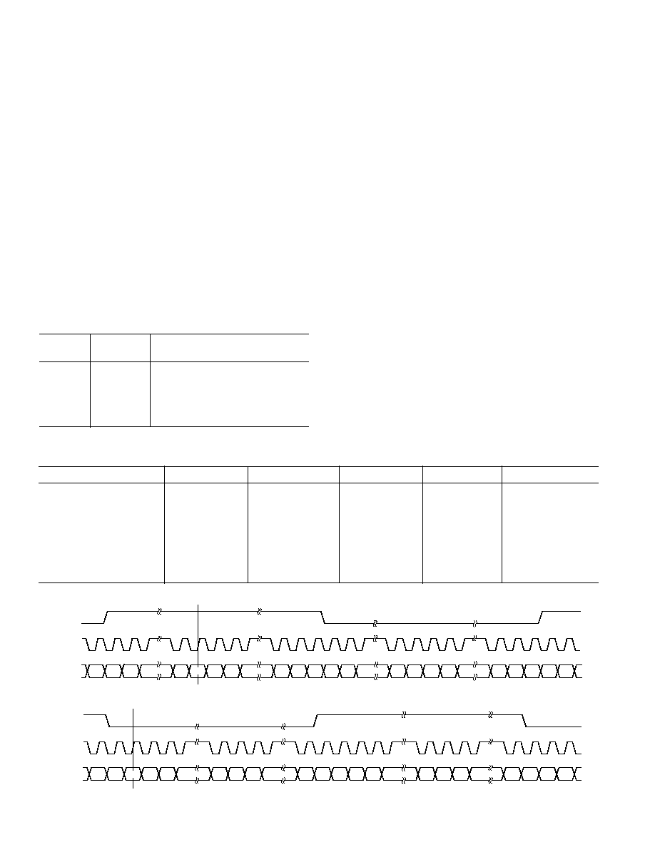
Table I. Serial Data Input Modes
IDPM1
IDPM0
(Pin 20)
(Pin 21)
Serial Data Input Format
0
0
Right Justified (16 Bits)
0
1
I
2
S-Compatible
1
0
Right Justified (20 Bits)
1
1
Right Justified (24 Bits)
Bit Clock
0
Left Justified
Figure 1 shows the right-justified mode (16-bit mode). L/RCLK
is HI for the left channel, LO for the right channel. Data is valid
on the rising edge of BCLK. The MSB is delayed 16-bit clock
periods from an L/RCLK transition, so that when there are 64
BCLK periods per L/RCLK period, the LSB of the data will be
right justified to the next L/RCLK transition. The right-justified
mode can also be used with 20-bit or 24-bit inputs as selected
in Table I.
Figure 2 shows the I
2
S-justified mode. L/RCLK is LO for the
left channel and HI for the right channel. Data is valid on the
rising edge of BCLK. The MSB is left justified to an L/RCLK
transition but with a single BCLK period delay. The I
2
S-justified
mode can be used with 16-/18-/20- or 24-bit inputs.
Figure 3 shows the left-justified mode. Note: Left-justified mode
is selected by pulsing IDPM1 (Pin 20) with bit clock, that is, tying
bit clock to IDPM1 while IDPM0 (Pin 21) is tied LO. Left-
justified can only be selected this way, it cannot be selected through
SPI Control Port.
L/RCLK is HI for the left channel, and LO for the right channel.
Data is valid on the rising edge of BCLK. The MSB is left-
justified to an L/RCLK transition, with no MSB delay. The
left-justified mode can be used with 16-/18-/20- or 24-bit inputs.
Note that the AD1854 is capable of a 32
× F
S
BCLK frequency
"packed mode" where the MSB is left-justified to an L/RCLK
transition, and the LSB is right-justified to an L/RCLK transi-
tion. L/RCLK is HI for the left channel, and LO for the right
channel. Data is valid on the rising edge of BCLK. Packed
mode can be used when the AD1854 is programmed in right-
justified mode. Packed mode is shown is Figure 4.
Table II. Frequency Mode Settings
F
S
96/48
MCLK
X2MCLK
384/256
Note
Normal, 32 kHz48 kHz
0
256
× F
S
0
0
Normal, 32 kHz48 kHz
0
384
× F
S
0
1
Normal, 32 kHz48 kHz
0
512
× F
S
1
0
Normal, 32 kHz48 kHz
0
1
1
Not Allowed
Double F
S
(96 kHz)
1
128
× F
S
0
0
Double F
S
(96 kHz)
1
(384/2)
× F
S
0
1
Double F
S
(96 kHz)
1
256
× F
S
1
0
Double F
S
(96 kHz)
1
1
1
Not Allowed
SDATA
INPUT
LSB
MSB2
MSB1
LSB+2 LSB+1
MSB2
MSB1
MSB
LSB+2 LSB+1
LSB
BCLK
INPUT
L/
RCLK
INPUT
LEFT CHANNEL
RIGHT CHANNEL
MSB
LSB
Figure 1. Right-Justified Mode
LEFT CHANNEL
RIGHT CHANNEL
MSB2
MSB1
LSB+2
LSB+1
LSB
MSB2
MSB1
MSB
LSB+2
LSB+1
LSB
MSB
L/
RCLK
INPUT
BCLK
INPUT
SDATA
INPUT
MSB
Figure 2. I
2
S-Justified Mode
AD1854
7
REV. A
MSB2
MSB1
LSB+2
LSB+1
LSB
MSB2
MSB1
MSB
LSB+2
LSB+1
LSB
MSB1
MSB
L/
RCLK
INPUT
BCLK
INPUT
SDATA
INPUT
LEFT CHANNEL
RIGHT CHANNEL
MSB
Figure 3. Left-Justified Mode
L/
RCLK
INPUT
LEFT CHANNEL
RIGHT CHANNEL
BCLK
INPUT
SDATA
INPUT
LSB
MSB1
MSB2
LSB+2
LSB+1
LSB
MSB
MSB1
MSB2
LSB+2
LSB+1
LSB
MSB
MSB1
MSB
Figure 4. 32
× F
S
Packed Mode
D15
D14
D0
t
CHD
t
CCH
t
CSU
t
CCL
t
CLL
t
CLH
CDATA
CCLK
CLATCH
t
CCP
Figure 5. Serial Control Port Timing
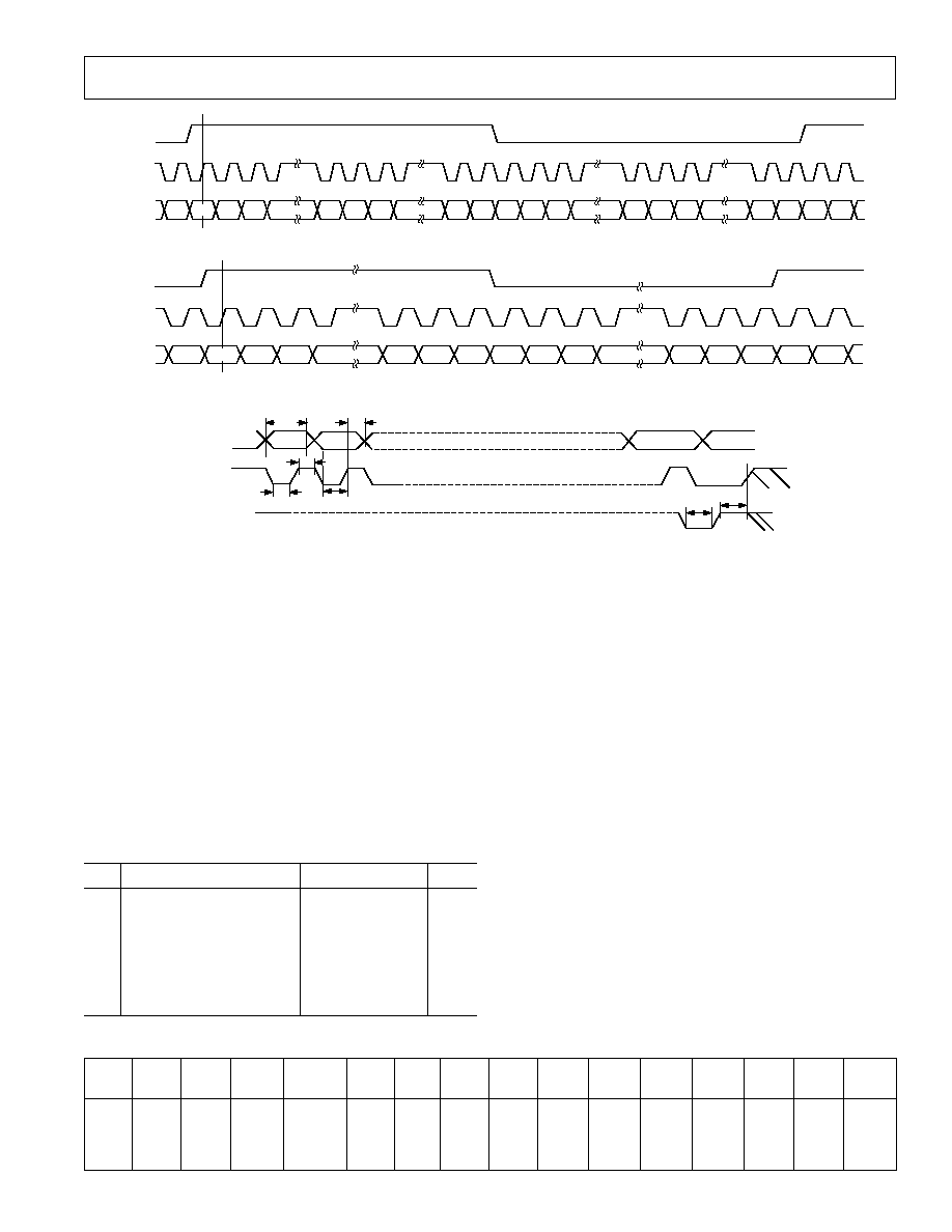
Serial Control Port
The AD1854 serial control port is SPI-compatible. SPI (Serial
Peripheral Interface) is an industry standard serial port protocol.
The write-only serial control port gives the user access to: select
input mode, soft power-down control, soft de-emphasis, channel-
specific attenuation and mute (both channels at once). The
AD1854 serial control port consists of three signals, control
clock CCLK (Pin 4), control data CDATA (Pin 5), and control
latch CLATCH (Pin 3). The control data input must be valid
on the control clock rising edge, and the control clock must make a
LO to HI transition when there is valid data. The control latch
must make a LO-to-HI transition after the LSB has been clocked
into the AD1854, while the control clock is inactive. The timing
relation between these signals is shown in Figure 5. The control
bits are assigned as in Table IV.
Table III. Digital Timing
Min
Unit
t
CCH
CCLK HI Pulsewidth
40 (Burst Mode)
ns
t
CCL
CCLK LO Pulsewidth
40 (Burst Mode)
ns
t
CCP
CCLK Period
80 (Burst Mode)
ns
t
CSU
CDATA Setup Time
10
ns
t
CHD
CDATA Hold Time
10
ns
t
CLL
CLATCH LO Pulsewidth
10
ns
t
CLH
CLATCH HI Pulsewidth
130 (Burst Mode)
ns
The serial control port is byte oriented. The data is MSB first,
and is unsigned. There is one control register for the left
channel or the right channel, as distinguished by Bit Data 10.
For power-up and reset, the default settings are: Data 11 the
mute control bit, reset default state is LO, which is the normal
(nonmuted) setting. Data 10 is LO, the Volume 9 through
Volume 0 control bits have a reset default value of 11 1111 1111,
which is an attenuation of 0.0 dB (i.e., full scale, no attenuation).
The intent with these reset defaults is to enable AD1854 applica-
tions without requiring the use of the serial control port. For those
users who do not use the serial control port, it is still possible to
mute the AD1854 output by using the MUTE (Pin 23) signal.
Note that the serial control port timing is asynchronous to the
serial data port timing. Changes made to the attenuator level
will be updated on the next edge of the L/RCLK after the
CLATCH write pulse as shown in Figure 8.
The SPI port can be used in either of two modes, Burst Mode,
or Continuous CCLK Mode, as described below.
Continuous CCLK Mode
In this mode, the maximum CCLK frequency is 3 MHz. The
CCLK can run continuously between transactions. Please note
that the LO-to-HI transition of the CLATCH with respect to
the rising edge of CCLK must be at least 130 ns, as shown in
Figure 6.
Table IV. Serial Control Bit Definitions
MSB
LSB
Data 15 Data 14
Data 13 Data 12
Data 11
Data 10 Data 9
Data 8
Data 7
Data 6
Data 5
Data 4
Data 3
Data 2
Data 1
Data 0
IDPM1
IDPM0
Soft
Soft
1/Mute
1/Right
Volume Volume
Volume
Volume
Volume
Volume
Volume
Volume
Volume Volume
Input
Input
Power-
De-
0/Normal
0/Left
Control Control
Control
Control
Control
Control
Control
Control
Control Control
Mode1
Mode0
Down
Emphasis (Nonmute)
Data
Data
Data
Data
Data
Data
Data
Data
Data
Data
Select
Select
8
AD1854
REV. A
Burst Mode
To operate with SPI CCLK frequencies up to 12.288 MHz, the
SPI port can be operated in Burst Mode. This means that when
CLATCH is high, CCLK cannot be HI, as shown in Figure 7.
Mute
The AD1854 offers two methods of muting the analog output.
By asserting the MUTE (Pin 23) signal HI, both the left and
right channel are muted. As an alternative, the user can assert
the mute bit in the serial control register (Data 11) HI. The
AD1854 has been designed to minimize pops and clicks when
muting and unmuting the device.
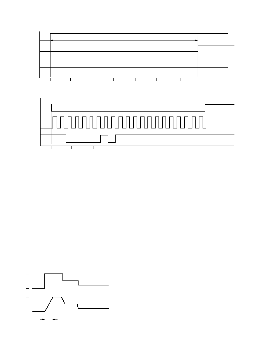
Smooth Volume Control with Auto Ramp Up/Down
The AD1854 incorporates ADI's 1024 step "Smooth Volume
Control" with auto ramp up/down. Once per L/RCLK cycle, the
AD1854 compares current volume level register to the volume
level request register Data 9:0. If different, volume is adjusted
one step/sample. Therefore, a change from max to min volume
takes 1024 samples or about 20 ms as shown in Figure 8.
20ms
TIME
60
60
0
0
LEVEL
dB
VOLUME REQUEST REGISTER
ACTUAL VOLUME REGISTER
Figure 8. Smooth Volume Control
Output Drive, Buffering and Loading
The AD1854 analog output stage is able to drive a 1 k
(in
series with 2 nF) load.
Power-Down Reset
The AD1854 offers two methods for power-down and reset.
When the PD/RST input (Pin 24) is asserted LO, the AD1854
is reset. As an alternative, the user can assert the soft power-
down bit (Data 13) HI. All the registers in the AD1854 digital
engine (serial data port, interpolation filter and modulator) are
zeroed. The two 8-bit registers in the serial control port are
initialized back to their default values. The user should wait
100 ms after bringing PD/RST HI before using the serial data
input port and the serial control input. The AD1854 is designed
to minimize pops and clicks when entering and exiting the power-
down state.
De-Emphasis
The AD1854 offers digital de-emphasis, supporting 50
µs/15 µs
digital de-emphasis intended for "Redbook" 44.1 kHz sample
frequency playback from Compact Discs. The AD1854 offers
control of de-emphasis by asserting the DEEMP input (Pin 9)
HI or by asserting the de-emphasis register bit (Data 12) HI.
The AD1854's de-emphasis is optimized for 44.1 kHz but will
scale to the other sample frequencies.
Control Signals
The IDPM0, IDPM1, and DEEMP control inputs are normally
connected HI or LO to establish the operating state of the
AD1854. They can be changed dynamically (and asynchronously
to L/RCLK and the master clock) as long as they are stable
before the first serial data input bit (i.e., MSB) is presented to
the AD1854.
CLATCH
CCLK
20
40
60
80
100
120
140
160
180
CDATA
>130ns
TIME ns
Figure 6. SPI Port Continuous CCLK Mode
CLATCH
CCLK
CDATA
TIME ns
200
400
600
800
1000
1200
1400
1600
1800
Figure 7. SPI Port Burst Mode
AD1854
9
REV. A
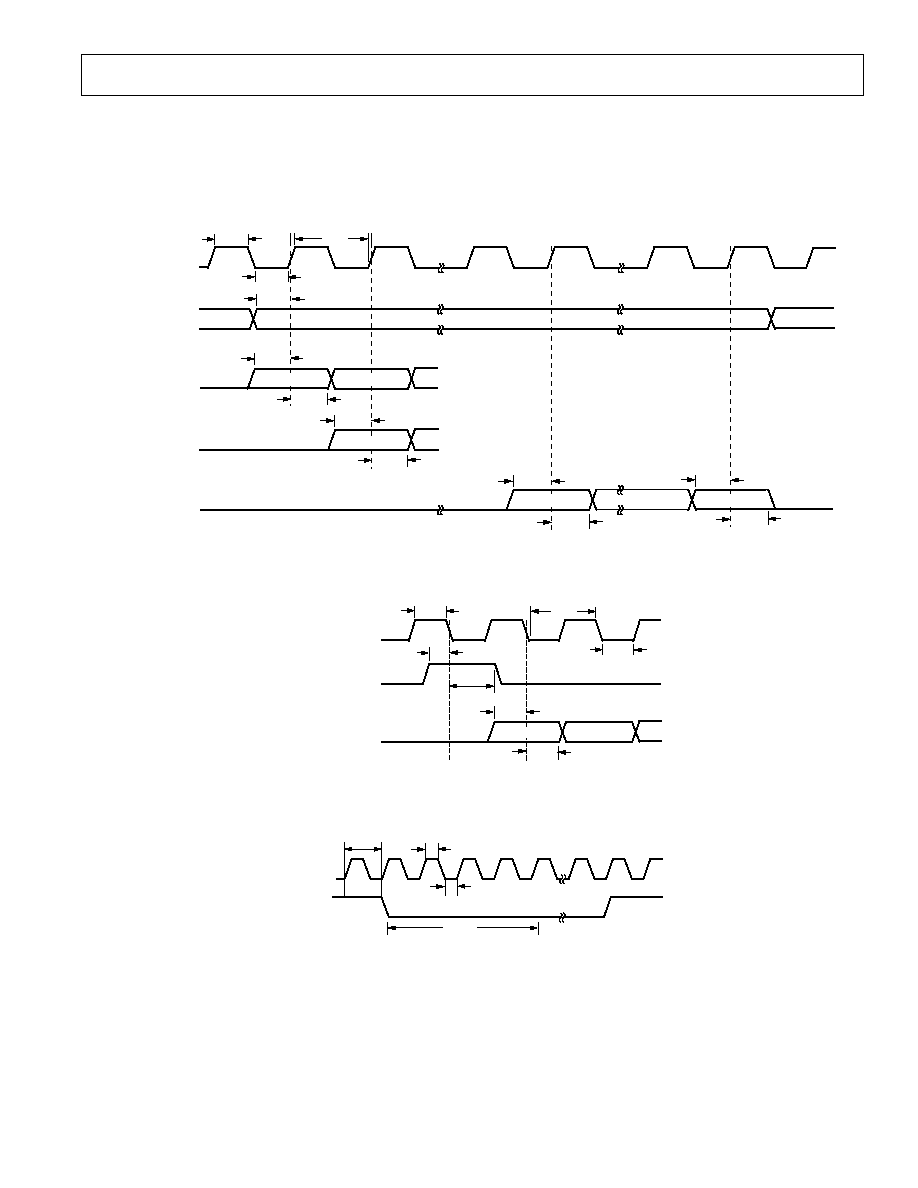
t
DLS
BCLK
L/
RCLK
SDATA
LEFT-JUSTIFIED
MODE
SDATA
RIGHT-JUSTIFIED
MODE
LSB
SDATA
I
2
S-JUSTIFIED
MODE
t
DBH
t
DBP
t
DBL
t
DDS
MSB
MSB-1
t
DDH
t
DDS
MSB
t
DDH
t
DDS
t
DDS
t
DDH
t
DDH
MSB
Figure 9. Serial Data Port Timing
BCLK
L/
RCLK
SDATA
LEFT-JUSTIFIED
DSP SERIAL
PORT STYLE MODE
MSB-1
t
DBH
t
DBP
t
DBL
t
DLS
t
DLH
t
DDS
t
DDH
MSB
Figure 10. Serial Data Port TimingDSP Serial Port Style Mode
PD/RST
MCLK
t
PDRP
t
DMP
t
DMH
t
DML
Figure 11.
Power-Down/Reset Timing
Timing Diagrams
The serial data port timing is shown in Figures 9 and 10. The
minimum bit clock HI pulsewidth is t
DBH
and the minimum bit
clock LO pulsewidth is t
DBL
. The minimum bit clock period is
t
DBP
. The left/right clock minimum setup time is t
DLS
and the
left/right clock minimum hold time is t
DLH
. The serial data
minimum setup time is t
DDS
and the minimum serial data hold
time is t
DDH
.
The power-down/reset timing is shown in Figure 11. The mini-
mum reset LO pulse width is t
PDRP
(four MCLK periods) to
accomplish a successful AD1854 reset operation.
10
AD1854
REV. A
I/F MODE
IDPM1 IDPM0
RJ, 16-BIT
0
0
I
2
S
0
1
RJ, 20-BIT
1
0
RJ, 24-BIT
1
1
LJ BCLK 0
U3B
SSM2135
C9
390pF
NP0
R8
953
R20
549
R9
2.15k
C14
1nF, NP0
R16
1.96k
C13
1nF, NP0
R10
953
R17
1.96k
R11
2.15k
C10
390pF
NP0
C15
2.2nF
NP0
LEFT
OUT
J1
1
C11
390pF
NP0
R12
953
R21
549
R13
2.15k
C17
1nF, NP0
R18
1.96k
C16
1nF, NP0
R14
953
R15
2.15k
C12
390pF
NP0
C18
2.2nF
NP0
RIGHT
OUT
J2
C6
100nF
AV
EE
C5
100nF
+AV
CC
3RD ORDER LP BESSEL FILTER
CORNER FREQUENCY: 92kHz
GROUP DELAY:
~
2.8 s
96/
48
384/
256
X2MCLK
SDATA
L/
RCLK
BCLK
MCLK
IDPM0
IDPM1
DEEMP
MUTE
CLATCH
CCLK
CDATA
ZEROR
ZEROL
PD/RST
DVDD
AVDD
OUTL+
OUTL
OUTR+
OUTR
FILTR
FITLB
DGND
AGND AGND
U1
AD1854JRS
C8
10 F
C1
100nF
+
C7
10 F
CLATCH
CCLK
CDATA
ZL
ZR
DE-EMPHASIS
MUTE
I/F
MODE
JP2
R5
10k
R4
10k
DVDD
RST
DGND
CDATA
CCLK
CLATCH
SDATA
LRCLK
SCLK
MCLK
JP1
MCLK/SR
SEL
R2
10k
R3
10k
DVDD
R1
10k
C3
100nF
DVDD
C2
100nF
AVDD
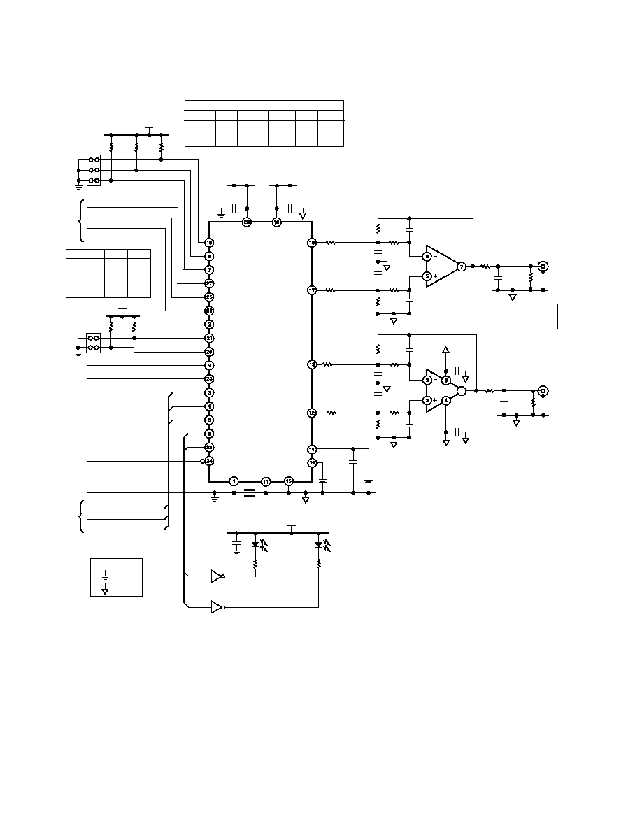
AD1854 STEREO DAC
OUTPUT BUFFERS AND LP FILTERS
MCLK/SR SELECT
SELECT RATE X2MCLK 384/
256 96/48
MCLK
SPDIF
DIRECT
DIRECT
44.1
48.0
96.0
0
0
0
0
0
0
0
0
1
11.2896
12.2880
12.2880
DVDD
U2A
HC04
1
2
ZL
U2B
HC04
3
4
ZR
R6
221
CR1
ZERO LEFT
C4
100nF
R7
221
CR2
ZERO RIGHT
FB1
600Z
+
NOTE:
= DGND
= AGND
SSM2135
1
R19
1.96k
U3A
AUDIO
DATA
CONTROL
PORT
53.6k
53.6k
Figure 12. Evaluation Board Circuit
AD1854
11
REV. A
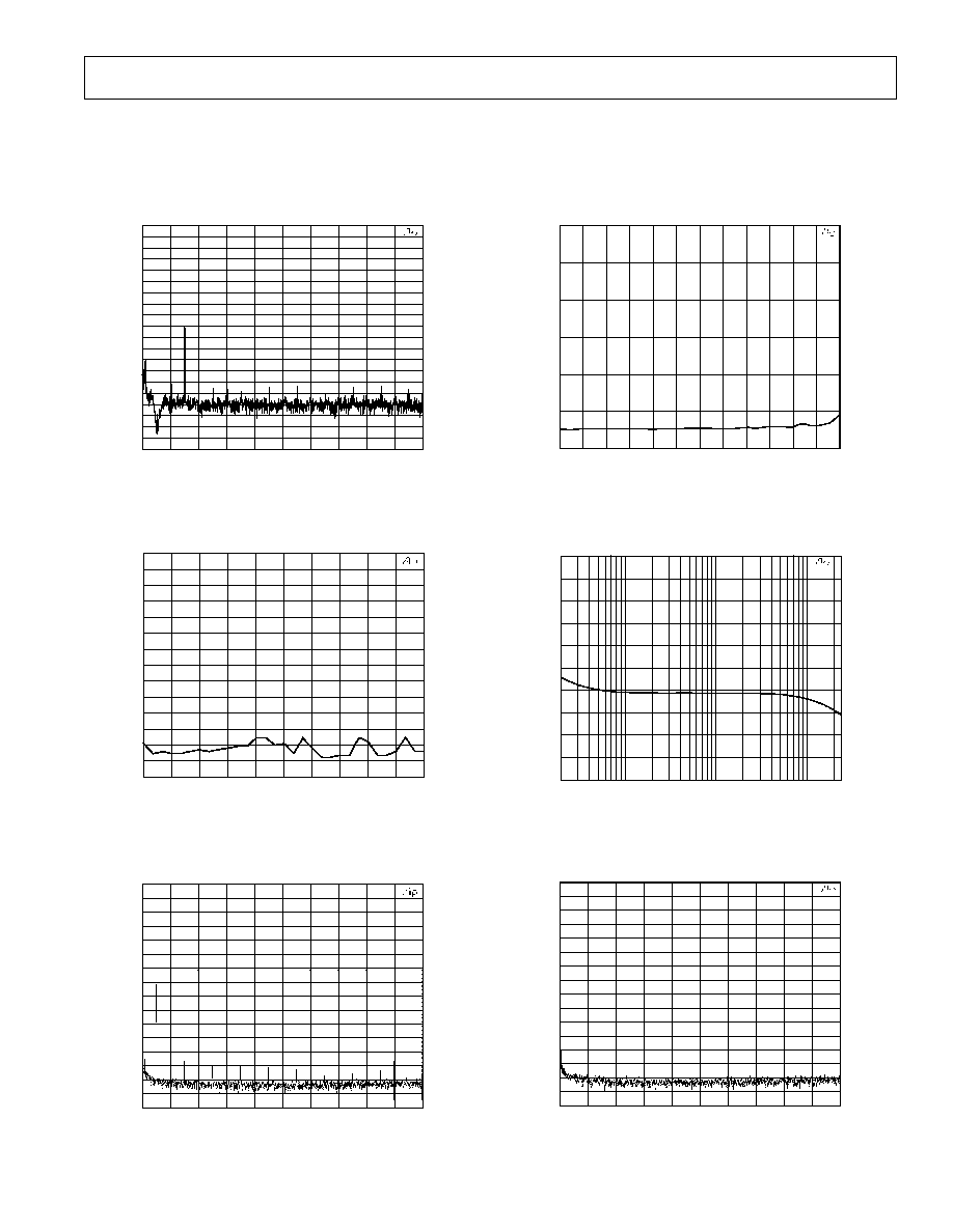
TYPICAL PERFORMANCE
Figures 13 through 20 illustrate the typical analog performance
of the AD1854 as measured by an Audio Precision System Two.
Signal-to-Noise and THD+N performance are shown under a
range of conditions. Figure 14 shows the power supply rejection
0
20
2
4
6
8
10
12
14
16
18
60
65
105
85
90
95
100
75
80
70
110
115
120
125
130
dBr
A
FREQUENCY kHz
135
140
145
150
155
160
60
65
105
85
90
95
100
75
80
70
110
115
120
125
130
dBr
B
135
140
145
150
155
160
Figure 13. THD+N at 1 kHz, 0.5 dBFS (8K-Point FFT)
0
20
2
4
6
8
10
12
14
16
18
40
45
85
65
70
75
80
55
60
50
100
105
dBr
A
FREQUENCY kHz
110
90
95
40
45
50
55
60
65
70
75
80
85
90
95
100
105
110
dBr
B
Figure 14. THD+N vs. Frequency at 0.5 dBFS
0
20
2
4
6
8
10
12
14
16
18
0
10
90
50
60
70
80
30
40
20
100
110
120
130
140
dBr
A
FREQUENCY kHz
150
160
0
10
90
50
60
70
80
30
40
20
100
110
120
130
140
dBr
B
150
160
Figure 15. Dynamic Range: 1 kHz at 60 dBFS
(8K Point FFT)
120
0
110 100 90 80 70 60 50 40 30
0
60
80
40
20
100
120
dBr
A
AMPLITUDE dBFS
20 10
0
20
40
60
80
100
120
dBr
B
Figure 16. THD+N vs. Level at 1 kHz
20
50
100
200
500
1k
dBr
A
2k
5k
10k
20k
FREQUENCY Hz
40
45
65
70
75
80
55
60
50
85
90
dBr
B
40
45
65
70
75
80
55
60
50
85
90
Figure 17. Power Supply Rejection to 300 mV p-p on AV
DD
0
20
2
4
6
8
10
12
14
16
18
0
10
90
50
60
70
80
30
40
20
100
110
120
130
140
dBr
A
FREQUENCY kHz
150
0
10
20
30
40
50
60
70
80
90
100
110
120
130
140
150
dBr
B
160
160
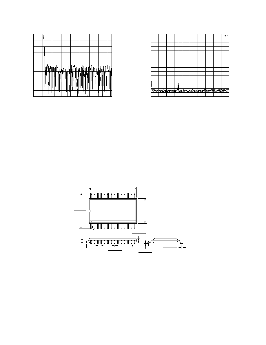
Figure 18. Noise Floor, A-Weighted (8K-Point FFT)
performance of the AD1854. Figure 15 shows the noise floor of
the AD1854. The digital filter transfer function is shown in
Figure 16. The two-tone test in Figure 17 is per the SMPTE
Standard for Measuring Intermodulation Distortion.
12
C3694
2.5
4/00 (rev. A)
PRINTED IN U.S.A.
AD1854
REV. A
FREQUENCY kHz
0
100
0
160
40
MAGNITUDE RESPONSE
dB
20
60
80
100
120
140
10
40
60
80
90
20
30
50
70
Figure 19. Digital Filter Response
OUTLINE DIMENSIONS
Dimensions shown in inches and (mm).
28-Lead Shrink Small Outline Package (SSOP)
(RS-28)
0.01 (0.25)
0.004 (0.09)
0.037 (0.95)
0.022 (0.55)
8°
0°
0.002
(0.05)
MIN
0.073 (1.85)
0.065 (1.65)
0.079 (2.0)
MAX
0.015 (0.38)
0.009 (0.22)
SEATING
PLANE
0.026
(0.65)
BSC
0.32 (8.20)
0.29 (7.40)
0.22 (5.60)
0.20 (5.00)
28
15
14
1
0.407 (10.34)
0.397 (10.08)
PIN 1
0
20
2
4
6
8
10
12
14
16
18
0
10
90
50
60
70
80
30
40
20
100
110
120
130
140
dBr
A
FREQUENCY kHz
150
0
10
20
30
40
50
60
70
80
90
100
110
120
130
140
150
dBr
B
Figure 20. Two-Tone Test