 | –≠–ª–µ–∫—Ç—Ä–æ–Ω–Ω—ã–π –∫–æ–º–ø–æ–Ω–µ–Ω—Ç: AD1858JRS | –°–∫–∞—á–∞—Ç—å:  PDF PDF  ZIP ZIP |
REV. 0
Information furnished by Analog Devices is believed to be accurate and
reliable. However, no responsibility is assumed by Analog Devices for its
use, nor for any infringements of patents or other rights of third parties
which may result from its use. No license is granted by implication or
otherwise under any patent or patent rights of Analog Devices.
a
AD1857/AD1858
Stereo, Single Supply
16-, 18- and 20-Bit Sigma-Delta DACs
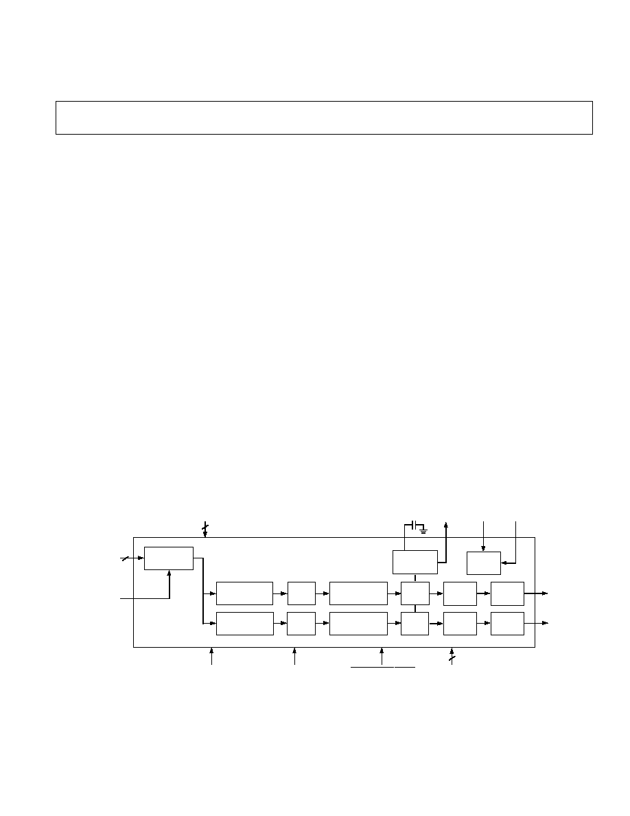
FUNCTIONAL BLOCK DIAGRAM
One Technology Way, P.O. Box 9106, Norwood, MA 02062-9106, U.S.A.
Tel: 617/329-4700
World Wide Web Site: http://www.analog.com
Fax: 617/326-8703
© Analog Devices, Inc., 1997
PRODUCT OVERVIEW
The AD1857/AD1858 are complete single-chip stereo digital
audio playback components. They each comprise an advanced
digital interpolation filter, a revolutionary "linearity-compensated"
multibit sigma-delta (
) modulator with dither, a jitter-tolerant
DAC, switched capacitor and continuous time analog filters and
analog output drive circuitry. Other features include digital
de-emphasis processing and mute. The AD1857/AD1858
support continuously variable sample rates with essentially
linear phase response, and support 50/15
µ
s digital de-emphasis
intended for "Redbook" 44.1 kHz sample frequency playback
from Compact Discs. The user must provide a master clock that
is synchronous with the left/right clock at 256 or 384 times the
intended sample frequency.
The AD1857/AD1858 have a simple but very flexible serial data
input port that allows for glueless interconnection to a variety of
ADCs, DSP chips, AES/EBU receivers and sample rate con-
verters. The AD1857 serial data input port can be configured
in either 16-bit, 18-bit or 20-bit left-justified or I
2
S-justified
modes. The AD1858 serial data input port can be configured in
either 16-bit right-justified or DSP serial port compatible modes.
The AD1857/AD1858 accept serial audio data in MSB first,
twos-complement format. A power-down mode is offered to
minimize power consumption when the device is inactive. The
AD1857/AD1858 operate from a single +5 V power supply.
They are fabricated on a single monolithic integrated circuit and
housed in 20-pin SSOP packages for operation over the
temperature range 0
∞
C to +70
∞
C.
FEATURES
Low Cost, High Performance Stereo DACs
128 Times Oversampling Interpolation Filter
Multibit
Modulator with Triangular PDF Dither
Discrete Time and Continuous Time Analog
Reconstruction Filters
Extremely Low Out-of-Band Energy
Buffered Outputs with 2 k
Output Load Drive
94 dB Dynamic Range, ≠90 dB THD+N Performance
Digital De-emphasis and Mute
0.1 C Maximum Phase Linearity Deviation
Continuously Variable Sample Rate Support
Power-Down Mode
16-, 18- and 20-Bit I
2
S-Justified, Left-Justified Modes
Offered on AD1857
Accepts 24-Bit Word
16-Bit Right-Justified and DSP Serial Port Modes
Offered on AD1858
Single +5 V Supply
20-Pin SSOP Package
APPLICATIONS
Digital Cable TV and Direct Broadcast Satellite Set-Top
Decoder Boxes
Video Laser Disk, Video CD and CD-I Players
High Definition Televisions, Digital Audio Broadcast
Receivers
CD, CD-R, DAT, DCC and MD Players
Digital Audio Workstations, Computer Multimedia
Products
MUTE
MUTE
MULTIBIT
MODULATOR
AD1857/AD1858
ANALOG
SUPPLY
DIGITAL
SUPPLY
16-/18-/20-BIT
DIGITAL
DATA INPUT
ANALOG
OUTPUTS
MUTE
CLOCK
MODE
CLOCK
IN
SERIAL
MODE
COMMON
MODE
2
4
3
DE-EMPHASIS
POWER-DOWN
/
RESET
128x
INTERPOLATION
FILTER
SERIAL DATA
INTERFACE
MULTIBIT
MODULATOR
128x
INTERPOLATION
FILTER
VOLTAGE
REFERENCE
ANALOG
FILTER
CLOCK
CIRCUIT
OUTPUT
BUFFER
ANALOG
FILTER
OUTPUT
BUFFER
DAC
DAC

TEST CONDITIONS UNLESS OTHERWISE NOTED
Supply Voltages (AV
DD
, DV
DD
)
+5.0 V
Ambient Temperature
25
∞
C
Input Clock (F
MCLK
)
11.2896 MHz (256
◊
F
S
Mode)
Input Signal
1.0013 kHz
≠0.5 dB Full Scale
Input Sample Rate
44.1 kHz
Measurement Bandwidth
20 Hz to 20 kHz
AD1857 Input Data Wordwidth
18 Bits
AD1858 Input Data Wordwidth
16 Bits
Load Capacitance
100 pF
Load Impedance
47 k
Input Voltage HI (V
IH
)
2.4 V
Input Voltage LO (V
IL
)
0.8 V
I
2
S-Justified Mode (Ref. Figure 7) for AD1857, Right-Justified Mode (Ref. Figure 8) for AD1858.
Performance of the right and left channels are identical (exclusive of the Interchannel Gain Mismatch and Interchannel Phase Deviation specifications).
Values in bold typeface are tested, all others are guaranteed, not tested.
ANALOG PERFORMANCE
Min
Typ
Max
Units
AD1857 Resolution
18
Bits
AD1858 Resolution
16
Bits
Dynamic Range (20 Hz to 20 kHz, ≠60 dB Input)
No A-Weight Filter
91
dB
With A-Weight Filter
94
dB
Total Harmonic Distortion + Noise
≠90
≠85
dB
0.003
0.006
%
Analog Outputs
Single-Ended Output Range (
±
Full Scale)
2.8
3.0
3.2
V p-p
Output Impedance at Each Output Pin
<200
Output Capacitance at Each Output Pin
20
pF
Out-of-Band Energy (0.5
◊
F
S
to 100 kHz)
≠72.5
dB
CMOUT
2.1
2.25
2.4
V
DC Accuracy
Gain Error
±
3.0
7.5
%
Interchannel Gain Mismatch
0.01
0.2
dB
Gain Drift
150
300
ppm/
∞
C
Interchannel Crosstalk (EIAJ method)
≠120
≠100
dB
Interchannel Phase Deviation
±
0.1
Degrees
Mute Attenuation
≠100
≠90
dB
De-emphasis Gain Error
±
0.1
dB
DIGITAL I/O
Min
Max
Units
Input Voltage HI (V
IH
)
2.4
V
Input Voltage LO (V
IL
)
0.8
V
Input Leakage (I
IH
@ V
IH
= 2.4 V)
10
µ
A
Input Leakage (I
IL
@ V
IL
= 0.8 V)
10
µ
A
Input Capacitance
20
pF
REV. 0
≠2≠
AD1857/AD1858≠SPECIFICATIONS

DIGITAL TIMING (Guaranteed over 0
∞
C to +70
∞
C, AV
DD
= DV
DD
= +5.0 V
±
5%)
Min
Max
Units
t
DML
MCLK LO Pulse Width (256
◊
F
S
Mode)
35
ns
t
DMH
MCLK HI Pulse Width (256
◊
F
S
Mode)
40
ns
t
DMP
MCLK Period (256
◊
F
S
Mode)
88.577
ns
t
DML
MCLK LO Pulse Width (384
◊
F
S
Mode)
25
ns
t
DMH
MCLK HI Pulse Width (384
◊
F
S
Mode)
25
ns
t
DMP
MCLK Period (384
◊
F
S
Mode)
59.0514
ns
t
DBH
BCLK HI Pulse Width
20
ns
t
DBL
BCLK LO Pulse Width
20
ns
t
DBP
BCLK Period
354.308
ns
t
DLS
L
RCLK Setup
20
ns
t
DLH
L
RCLK Hold
5
ns
t
DDS
SDATA Setup
5
ns
t
DDH
SDATA Hold
10
ns
t
PDRP
PD/RST LO Pulse Width
4 MCLK Periods
ns
(355 ns @ 11.2896 MHz)
POWER
Min
Typ
Max
Units
Supplies
Voltage, Analog and Digital
4.75
5
5.25
V
Analog Current
35
40
mA
Analog Current ≠ Power-Down
30
60
µ
A
Digital Current
20
25
mA
Digital Current ≠ Power-Down
5
11
mA
Dissipation
Operation ≠ Both Supplies
275
325
mW
Operation ≠ Analog Supply
175
200
mW
Operation ≠ Digital Supply
100
125
mW
Power-Down ≠ Both Supplies
25
56
mW
Power Supply Rejection Ratio
1 kHz 300 mV p-p Signal at Analog Supply Pins
≠60
dB
20 kHz 300 mV p-p Signal at Analog Supply Pins
≠50
dB
TEMPERATURE RANGE
Min
Typ
Max
Units
Specifications Guaranteed
25
∞
C
Functionality Guaranteed
0
70
∞
C
Storage
≠55
125
∞
C
ABSOLUTE MAXIMUM RATINGS*
Min
Typ
Max
Units
DV
DD
to DGND
≠0.3
6
V
AV
DD
to AGND
≠0.3
6
V
Digital Inputs
DGND ≠ 0.3
DV
DD
+ 0.3
V
Analog Outputs
AGND ≠ 0.3
AV
DD
+ 0.3
V
AGND to DGND
≠0.3
0.3
V
Reference Voltage
Indefinite Short Circuit to Ground
Soldering
+300
∞
C
10
sec
*Stresses greater than those listed under Absolute Maximum Ratings may cause permanent damage to the device. This is a stress rating only; functional operation of the
device at these or any other conditions above those indicated in the operational section of this specification is not implied. Exposure to absolute maximum rating conditions
for extended periods may affect device reliability.
REV. 0
≠3≠
AD1857/AD1858
AD1857/AD1858
REV. 0
≠4≠
PACKAGE CHARACTERISTICS
Min
Typ
Max
Units
JA
(Thermal Resistance [Junction-to-Ambient])
195
∞
C/W
JC
(Thermal Resistance [Junction-to-Case])
13
∞
C/W
DIGITAL FILTER CHARACTERISTICS
Min
Max
Units
Passband Ripple
±
0.045
dB
Stopband
1
Attenuation
62
dB
48 kHz F
S
Passband
0
21.312
kHz
Stopband
26.688
6117
kHz
44.1 kHz F
S
Passband
0
19.580
kHz
Stopband
24.520
5620
kHz
32 kHz F
S
Passband
0
14.208
kHz
Stopband
17.792
4078
kHz
Other F
S
Passband
0
0.444
F
S
Stopband
0.556
127.444
F
S
Group Delay
40/F
S
sec
Group Delay Variation
0
µ
s
ANALOG FILTER CHARACTERISTICS
Min
Typ
Max
Units
Passband Ripple
≠0.075
dB
Stopband Attenuation (at 64
◊
F
S
)
58
dB
NOTES
1
Stopband nominally repeats itself at multiples of 128
◊
F
S
, where F
S
is the input word rate. Thus the digital filter will attenuate to 62 dB across the frequency
spectrum, except for a range
±
0.55
◊
F
S
wide at multiples of 128
◊
F
S
.
Specifications subject to change without notice.
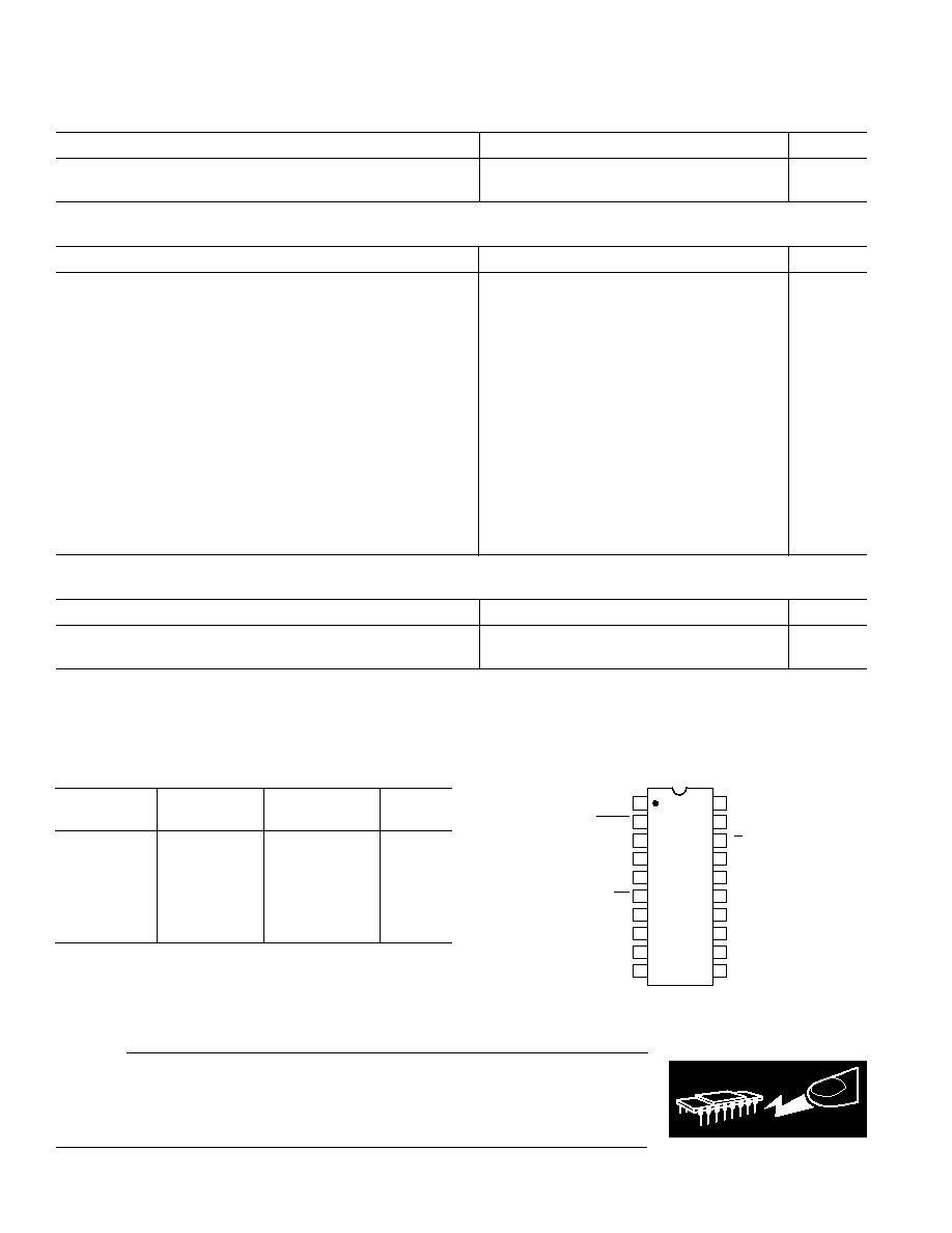
PIN CONFIGURATION
ORDERING GUIDE
Package
Package
Model
Temperature
Description
Option*
AD1857JRS
0
∞
C to +70
∞
C
20-Lead SSOP
RS-20
AD1857JRSRL
0
∞
C to +70
∞
C
20-Lead SSOP
RS-20 on
13" Reels
AD1858JRS
0
∞
C to +70
∞
C
20-Lead SSOP
RS-20
AD1858JRSRL
0
∞
C to +70
∞
C
20-Lead SSOP
RS-20 on
13" Reels
*RS = Shrink Small Outline
WARNING!
ESD SENSITIVE DEVICE
CAUTION
ESD (electrostatic discharge) sensitive device. Electrostatic charges as high as 4000 V readily
accumulate on the human body and test equipment and can discharge without detection. Although
the AD1857/AD1858 feature proprietary ESD protection circuitry, permanent damage may occur on
devices subjected to high energy electrostatic discharges. Therefore, proper ESD precautions are
recommended to avoid performance degradation or loss of functionality.
14
13
12
11
17
16
15
20
19
18
10
9
8
1
2
3
4
7
6
5
TOP VIEW
(Not to Scale)
AD1857
AD1858
NC = NO CONNECT
MCLK
DV
DD
L
R
CLK
BCLK
SDATA
PD
/
RST
MODE
NC
AV
DD
MUTE
DGND
DEEMP
384/
256
AV
DD
OUTL
AGND
CMOUT
FILT
AGND
OUTR

AD1857/AD1858
REV. 0
≠5≠
PIN LIST
Digital Audio Serial Input Interfaces
Pin Name
Number
I/O
Description
SDATA
20
I
Serial input, MSB first, containing two channels of 16, 18 or 20 bits (AD1857) or
16 bits (AD1858) of twos complement data per channel.
BCLK
19
I
Bit clock input for input data. Need not run continuously; may be gated or used in a
burst fashion.
L
RCLK
18
I
Left/
right clock input for input data. Must run continuously.
MODE
3
I
Input serial data port mode control. Selects between I
2
S-justified (HI) and left-justified
(LO) on the AD1857. Selects between DSP serial port style mode (HI) and right-
justified (LO) on the AD1858. The state of the mode pin should be changed only when
the AD1857/AD1858 is held in reset (
PD/RST LO). Otherwise, the AD1857/
AD1858 serial port may lose synchronism.
Control and Clock Signals
Pin Name
Number
I/O
Description
PD/RST
2
I
Power-Down/Reset. The AD1857/AD1858 are placed in a low power consumption
"sleep" mode when this pin is held LO. The AD1857/AD1858 are reset on the
rising edge of this signal. Connect HI for normal operation.
DEEMP
5
I
De-emphasis. Digital de-emphasis is enabled when this input signal is HI. This is
used to impose a 50/15
µ
s response characteristic on the output audio spectrum at
an assumed 44.1 kHz sample rate.
MUTE
15
I
Mute. Assert HI to mute both stereo analog outputs of the AD1857/AD1858.
Deassert LO for normal operation.
MCLK
1
I
Master Clock Input. Connect to an external clock source at either 256 or 384 times
the intended sample frequency as determined by the 384/
256 pin. Must be synchro-
nous with L
RCLK, but may have any phase with respect to LRCLK.
384/
256
6
I
Selects the master clock mode as either 384 times the intended sample frequency
(HI) or 256 times the intended sample frequency (LO). The state of this input
should be hardwired to logic LO or logic HI or may be changed while the AD1857/
AD1858 is in power-down/reset. It must not be changed while the AD1857/AD1858
is operational.
Analog Signals
Pin Name
Number
I/O
Description
FILT
11
O
Voltage Reference Filter Capacitor Connection. Bypass and decouple the voltage
reference with parallel 10
µ
F and 0.1
µ
F capacitors to the AGND pin.
CMOUT
10
O
Voltage Reference Common Mode Output. Should be decoupled with 10
µ
F
capacitor to the AGND pin or plane. This output is available externally for dc
coupling and level-shifting. CMOUT should not have any signal dependent load,
or used where it will sink or source current.
OUTL
8
O
Left channel line level analog output.
OUTR
13
O
Right channel line level analog output.
Power Supply Connections and Miscellaneous
Pin Name
Number
I/O
Description
AV
DD
7, 14
I
Analog Power Supply. Connect to analog +5 V supply.
AGND
9, 12
I
Analog Ground.
DV
DD
17
I
Digital Power Supply. Connect to digital +5 V supply.
DGND
16
I
Digital Ground.
N/C
4
No Connect. Reserved. Do not connect.

AD1857/AD1858
REV. 0
≠6≠
DEFINITIONS
Dynamic Range
The ratio of a full-scale output signal to the integrated output
noise in the passband (0 kHz to 20 kHz), expressed in decibels
(dB). Dynamic range is measured with a ≠60 dB input signal
and is equal to (S/[THD+N]) + 60 dB. Note that spurious
harmonics are below the noise with a ≠60 dB input, so the noise
level establishes the dynamic range. This measurement tech-
nique is consistent with the recommendations of the Audio
Engineering Society (AES17-1991) and the Electronic Industries
Association of Japan (EIAJ CP-307).
Total Harmonic Distortion + Noise (THD+N)
The ratio of the root-mean-square (rms) value of a full-scale
fundamental input signal to the rms sum of all other spectral
components in the passband, expressed in decibels (dB) and
as a percentage.
Passband
The region of the frequency spectrum unaffected by the
attenuation of the digital interpolation filter.
Passband Ripple
The peak-to-peak variation in amplitude response from equal-
amplitude input signal frequencies within the passband,
expressed in decibels.
Stopband
The region of the frequency spectrum attenuated by the digital
interpolation filter to the degree specified by "stopband
attenuation."
Gain Error
With a near full-scale input, the ratio of actual output to
expected output, expressed as a percentage.
Interchannel Gain Mismatch
With identical near full-scale inputs, the ratio of outputs of the
two stereo channels, expressed in decibels.
Gain Drift
Change in response to a near full-scale input with a change in
temperature, expressed as parts-per-million (ppm) per
∞
C.
Crosstalk (EIAJ Method)
Ratio of response on one channel with a zero input, to a full-
scale 1 kHz sine-wave input on the other channel, expressed in
decibels.
Interchannel Phase Deviation
Difference in output sampling times between stereo channels,
expressed as a phase difference in degrees between 1 kHz
inputs.
Power Supply Rejection
With zero input, signal present at the output when a 300 mV
p-p signal is applied to power supply pins, expressed in decibels
of full scale.
Group Delay
Intuitively, the time interval required for an input pulse to
appear at the converter's output, expressed in seconds(s). More
precisely, the derivative of radian phase with respect to radian
frequency at a given frequency.
Group Delay Variation
The difference in group delays at different input frequencies.
Specified as the difference between the largest and the smallest
group delays in passband, expressed in microseconds (
µ
s).
De-Emphasis Gain Error
A measure, expressed in decibels, of the difference between the
ideal 50/15
µ
s de-emphasis filter response, and the actual 50/15
µ
s
de-emphasis filter response.
AD1857/AD1858
REV. 0
≠7≠
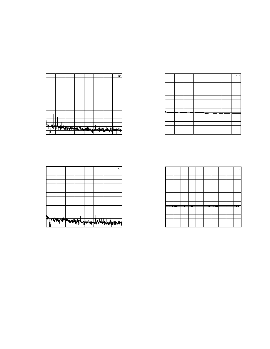
Typical Performance Characteristics
Figures 1 through 4 illustrate the typical performance of the
AD1857/AD1858 as measured by an Audio Precision System
Two. Signal-to-Noise (dynamic range) THD+N performance is
shown under a range of conditions. Figure 5 shows the power
supply rejection performance of the AD1857/AD1858. The
channel separation performance of the AD1857/AD1858 is
shown in Figure 6. The digital filter transfer function is shown
in Figure 7.
kHz
dBr A
0
≠100
0
2.5
20.0
5.0
7.5
10.0
12.5
15.0
17.5
≠10
≠40
≠50
≠70
≠90
≠20
≠30
≠60
≠80
≠120
≠130
≠140
≠150
≠110
Figure 1. 1 kHz Tone at ≠0.5 dBFS
kHz
dBr A
0
≠100
0
2.5
20.0
5.0
7.5
10.0
12.5
15.0
17.5
≠10
≠40
≠50
≠70
≠90
≠20
≠30
≠60
≠80
≠120
≠130
≠140
≠110
Figure 2. 1 kHz Tone at ≠10 dBFS
kHz
dBr A
0
≠100
0
2.5
20.0
5.0
7.5
10.0
12.5
15.0
17.5
≠10
≠40
≠50
≠70
≠90
≠20
≠30
≠60
≠80
≠120
≠130
≠140
≠110
Figure 3. THD+N vs. Frequency at ≠0.5 dBFS
dBFS
dBr A
0
≠100
≠100
≠20
≠80
≠60
≠40
≠10
≠40
≠50
≠70
≠90
≠20
≠30
≠60
≠80
≠120
≠130
≠140
≠110
0
Figure 4. THD+N vs. Amplitude at 1 kHz

AD1857/AD1858
REV. 0
≠8≠
Typical Performance Characteristics (continued)
kHz
dBr A
≠70
0
2.5
20.0
RIGHT CHANNEL
5.0
7.5
10.0
12.5
15.0
17.5
≠40
≠45
≠55
≠65
≠50
≠60
≠80
≠75
≠40
≠44
≠48
≠52
≠56
≠60
≠64
≠68
≠72
≠76
≠80
dBr B
LEFT CHANNEL
Figure 5. Power Supply Rejection to 300 mV p-p on AV
DD
kHz
dBr A
0
≠100
0
2.5
20.0
5.0
7.5
10.0
12.5
15.0
17.5
≠10
≠40
≠50
≠70
≠90
≠20
≠30
≠60
≠80
≠120
≠130
≠140
≠110
Figure 6. Channel Separation vs. Frequency at ≠0.5 dBFS
0.0
3.5
0.5
1.0
1.5
2.0
2.5
3.0
0
≠10
≠90
≠50
≠60
≠70
≠80
≠30
≠40
≠20
≠100
≠110
≠120
≠130
≠140
≠150
≠160
dBFS
F
S
Figure 7. Digital Filter Signal Transfer Function to 3.5 F
S

AD1857/AD1858
REV. 0
≠9≠
THEORY OF OPERATION
The AD1857/AD1858 offer the advantages of sigma-delta con-
version architectures (no component trims, low cost CMOS
process technology, superb low-level linearity performance) with
the advantages of conventional multibit R-2R resistive ladder
audio DACs (continuously variable sample rate support, jitter
tolerance, very low output noise, etc.).
The use of a multibit sigma-delta modulator means that the
AD1857/AD1858 generate dramatically lower amounts of out-
of-band noise energy, which greatly reduces the requirement on
post DAC filtering. The required post-filtering is integrated on
the AD1857/AD1858. The AD1857/AD1858's multibit sigma-
delta modulator is also highly immune to digital substrate noise.
Serial Audio Data Interface
The serial audio data interface uses the bit clock (BCLK) simply
to clock the data into the AD1857/AD1858. The bit clock may
therefore be asynchronous to the L/
R clock. The left/right clock
(L
RCLK) is both a framing signal and the sample frequency
input to the interpolation filter. The left/
right clock must be
synchronous with MCLK, but may have any phase relationship
with respect to MCLK; L
RCLK is generally synchronously divided
down from MCLK. The SDATA input carries the serial stereo
digital audio in MSB first, twos-complement format.
Digital Interpolation Filter
The purpose of the interpolator is to "oversample" the input
data, i.e., to increase the sample rate so the first signal image is
moved out to the oversample frequency, which relaxes the
attenuation requirements on the analog reconstruction filter.
The AD1857/AD1858 interpolator increases the input data
sample rate by 128. The interpolation is performed using a
multistage FIR digital filter structure. The first stage is a droop
equalizer; the second and third stages are halfband filters; and
the fourth stage is a second-order comb filter. The FIR filter
implementation is multiplier-free, i.e., the multiplies are performed
using shift-and-add operations. The FIR filter coefficients have
been recoded in a canonical sign digit format to enable the use
of a compact arithmetic logic unit without a multiplier.
Multibit Sigma-Delta Modulator
The AD1857/AD1858 employ a 4-bit second-order sigma-delta
modulator. Whereas a traditional single-bit sigma-delta
modulator has two levels of quantization, the AD1857/AD1858's
has 17 levels of quantization. Traditional single-bit sigma-delta
modulators sample the input signal at 64 times the input sample
rate; the AD1857/AD1858 sample the input signal at 128 times
the input sample rate. The additional quantization levels
combined with the high oversampling ratio means that the
AD1857/AD1858 DAC output spectrum contains dramatically
lower levels of out-of-band noise energy, which is a major
stumbling block with more traditional single-bit sigma-delta
architectures. This means that the post-DAC analog reconstruction
filter has reduced transition band steepness and attenuation
requirements, which directly equates to lower phase distortion.
Since the analog filtering generally establishes the noise and
distortion characteristic of the DAC, the reduced requirements
translate into better audio performance.
Multibit sigma-delta modulators bring an additional benefit:
they are essentially free of stability (and therefore potential loop
oscillation) problems. They are able to scale the output signal
to a wider range of the voltage reference, which can increase the
overall dynamic range of the converter.
The conventional problem limiting the performance of multibit
sigma-delta converters is the nonlinearity of the passive circuit
elements used to sum the quantization levels. Analog Devices has
developed (and received patents on) a revolutionary architecture
that overcomes the circuit element linearity problem that otherwise
limits the performance of multibit sigma-delta audio converters.
This new architecture provides the AD1857/AD1858 with the
same excellent differential nonlinearity and linearity drift (over
temperature and time) specifications as single bit sigma-delta
DACs.
The AD1857/AD1858's multibit modulator has another
important advantage; it has a high immunity to substrate digital
noise. Substrate noise can be a significant problem in mixed-
signal designs, where it can produce intermodulation products
that fold down into the audio band. The AD1857/AD1858 are
approximately eight times less sensitive to digital substrate noise
(voltage reference noise injection) than equivalent single-bit
sigma-delta modulator based DACs.
Dither Generator
The AD1857/AD1858 include an on-chip dither generator that
is intended to further "whiten" the quantization noise introduced
by the multibit DAC. The dither has a triangular Probability
Distribution Function (PDF) characteristic, which is generally
considered to create the most favorable noise shaping of the
residual quantization noise. The AD1857/AD1858 are among the
first low cost IC audio DACs to include dithering.
Analog Filtering
The AD1857/AD1858 include a second-order switched
capacitor discrete time low-pass filter followed by a first-order
analog continuous time low-pass filter. These filters eliminate
the need for any additional off-chip external reconstruction
filtering. This on-chip switched capacitor analog filtering is
essential to reduce the deleterious effects of master clock jitter.
Digital De-Emphasis Processing
The AD1857/AD1858 include digital circuitry for implementing
the 50/15
µ
s de-emphasis frequency response characteristic. A
control pin DEEMP (Pin 5) enables de-emphasis when it is
asserted HI. The digital de-emphasis response assumes a sample
frequency of 44.1 kHz. The transfer function magnitude error
of this digital filter is less than
±
0.1 dB (from 0 kHz to 20 kHz)
compared to a 50/15
µ
s continuous time filter. If the sample
frequency is not 44.1 kHz, the de-emphasis frequency response
will scale directly with frequency. The 44.1 kHz F
S
digital de-
emphasis frequency response is shown in Figure 8.
GAIN ≠ dB
0
≠10
F1
3.183
F2
10.61
T1 = 50µs
T2 = 15µs
FREQUENCY ≠ kHz
Figure 8. Digital De-Emphasis Frequency Response
AD1857/AD1858
REV. 0
≠10≠
OPERATING FEATURES
Serial Data Input Port
The AD1857/AD1858 use the frequency of the left/
right and
master input clocks to determine the input sample rate. Gen-
erally, the master clock (MCLK) is divided down to synthesize
the left/
right clock (LRCLK). LRCLK must run continuously
and transition twice per stereo sample period (except in the left-
justified DSP serial port style mode, when it transitions four
times per stereo sample period). The bit clock (BCLK) is edge-
sensitive and may be used in a gated or burst mode, i.e., a
stream of pulses during data transmission followed by periods of
inactivity. The bit clock is only used to write the audio data
into the serial input port. It is important that the left/
right clock
is "clean," with monotonic rising and falling edge transitions
and no excessive overshoot or undershoot that could cause false
clock triggering of the AD1857/AD1858.
The AD1857/AD1858's flexible serial data input port accepts
data in twos-complement, MSB first format. The left channel
data field always precedes the right channel data field. The
input data consists of 16, 18 or 20 bits (16 bits only to the
AD1858). All digital inputs are specified to TTL logic levels.
The input data port is configured by a control pin, MODE,
Pin 3. The AD1857 and the AD1858 are identical except for
the serial data input port modes offered. The AD1857 offers
I
2
S-justified and left-justified modes, for 16-, 18- or 20-bit data
words. The AD1858 offers right-justified and DSP serial port
style mode for 16-bit data words.
Note: During the first 30,000 MCLK cycles after coming out of
reset, the AD1857/AD1858 synchronizes its internal sequencer
counter to the incoming L
RCLK. After this period of time, it is
assumed that the L
RCLK and the internal AD1857/AD1858
output channels could be switched (L to
R and R to L). Therefore,
if the incoming L
RCLK is stopped and then restarted with a
different phase, the AD1857/AD1858 should be reset again to
synchronize with this new clock.
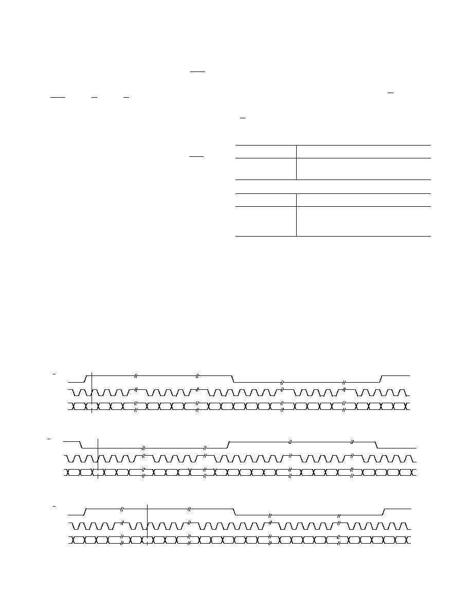
Serial Input Port Modes
The AD1857/AD1858 use an input pin to control the mode
configuration of the input data port. MODE (Pin 3) programs
the input data port mode as follows:
Figure 9 shows the AD1857 left-justified mode. L
RCLK is HI
for the left channel, and LO for the right channel. Data is valid
on the rising edge of BCLK. The MSB is left-justified to an
L
RCLK transition, with no MSB delay. The left-justified mode
can be used in the 16-, 18- or 20-bit input mode.
MODE (Pin 3)
AD1857 Serial Input Port Mode
LO
Left-Justified (See Figure 9)
HI
I
2
S-Justified (See Figure 10)
MODE (Pin 3)
AD1858 Serial Input Port Mode
LO
Right-Justified (See Figure 11)
HI
Left-Justified DSP Serial Port Style
(See Figure 12)
Figure 10 shows the AD1857 I
2
S-justified mode. L
RCLK is
LO for the left channel, and HI for the right channel. Data is
valid on the rising edge of BCLK. The MSB is left-justified to
an L
RCLK transition, but with a single BCLK period delay.
The I
2
S-justified mode can be used in the 16-, 18- or 20-bit
input mode.
Figure 11 shows the AD1858 the right-justified mode. L
RCLK
is HI for the left channel, and LO for the right channel. Data is
valid on the rising edge of BCLK. The MSB is delayed 16-bit
clock periods from an L
RCLK transition so that when there are
64 BCLK periods per L
RCLK period, the LSB of the data will
be right-justified to the next L
RCLK transition.
LEFT CHANNEL
RIGHT CHANNEL
BCLK
INPUT
SDATA
INPUT
LRCLK
INPUT
MSB
MSB-1
MSB-2
LSB+2
LSB+1
LSB
MSB-1
MSB-2
LSB+2
LSB+1
LSB
MSB
MSB-1
MSB
Figure 9. AD1857 Left-Justified Mode
LRCLK
INPUT
BCLK
INPUT
SDATA
INPUT
LEFT CHANNEL
RIGHT CHANNEL
MSB
MSB-1
MSB-2
LSB+2
LSB+1
LSB
MSB-1
MSB-2
LSB+2
LSB+1
LSB
MSB
MSB
Figure 10. AD1857 I
2
S-Justified Mode
LEFT CHANNEL
RIGHT CHANNEL
BCLK
INPUT
SDATA
INPUT
LRCLK
INPUT
MSB
MSB-1 MSB-2
LSB+2 LSB+1
LSB
MSB-1 MSB-2
LSB+2 LSB+1
LSB
MSB
LSB
Figure 11. AD1858 Right-Justified Mode
AD1857/AD1858
REV. 0
≠11≠
LEFT CHANNEL
RIGHT CHANNEL
BCLK
INPUT
SDATA
INPUT
LRCLK
INPUT
MSB
MSB-1
LSB+2
LSB+1
LSB
MSB-1
LSB+2
LSB+1
LSB
MSB
MSB-1
MSB
Figure 12. AD1858 Left-Justified DSP Serial Port Style
LEFT CHANNEL
RIGHT CHANNEL
BCLK
INPUT
SDATA
INPUT
LRCLK
INPUT
MSB
MSB-1
LSB+2
LSB+1
LSB
MSB-1
MSB-2
LSB+2
LSB+1
LSB
MSB
MSB-1
LSB
MSB-2
MSB
Figure 13. AD1857/AD1858 32 F
S
Packed Mode
Figure 12 shows the AD1858 left-justified DSP serial port style
mode. L
RCLK must pulse HI for at least one bit clock period
before the MSB of the left channel is valid, and L
RCLK must
pulse HI again for at least one bit clock period before the MSB
of the right channel is valid. Data is valid on the falling edge of
BCLK. Note that in this mode, it is the responsibility of the DSP
to ensure that the left data is transmitted with the first L
RCLK
pulse, the right data is transmitted with the second L
RCLK pulse,
and synchronism is maintained from that point forward.
Note that in 16-bit input mode, the AD1857/AD1858 are
capable of a 32
◊
F
S
BCLK frequency "packed mode" where
the MSB is left-justified to an L
RCLK transition, and the LSB
is right-justified to an L
RCLK transition. LRCLK is HI for the
left channel, and LO for the right channel. Data is valid on the
rising edge of BCLK. Packed mode can be used when the
AD1857 is programmed in left-justified mode, or when the
AD1858 is programmed in right-justified mode. Packed mode
is shown in Figure 13.
Master Clock
The synchronous master clock of the AD1857/AD1858 is
supplied by an external clock source applied to MCLK. Figure
14 shows example connections. Do not change the state of the
384/
256 pin while the AD1857/AD1858 is operational; this pin
should be hardwired LO or HI. Alternatively, its state may be
changed while the
PD/RST pin is asserted LO.
1
MCLK
6
256 MODE
384 MODE
SAMPLE RATE
12.288MHz
18.432MHz
48kHz
44.1kHz
32kHz
11.2896MHz
16.9344MHz
8.192MHz
12.288MHz
384/
256
MCLK FREQUENCY
384/
256
= LO
384/
256
= HI
Figure 14. AD1857/AD1858 Clock Connections
Digital Mute
The AD1857/AD1858 offer a control pin that mutes the analog
output. By asserting the MUTE (Pin 15) signal HI, both the
left channel and the right channel are muted. The AD1857/
AD1858 have been designed to minimize pops and clicks when
muting and unmuting the device. The AD1857/AD1858
include a zero crossing detector which attempts to implement
mute on waveform zero crossings only. If a zero crossing is not
found within 1024 input sample periods (approximately 23
milliseconds at 44.1 kHz), the output is muted regardless.
Output Drive, Buffering and Loading
The AD1857/AD1858 analog output stage is able to drive a 2 k
load. If lower impedance loads must be driven, an external
buffer stage such as the Analog Devices SSM2142 should be
used. The analog output is generally ac coupled with a 10
µ
F
capacitor as shown in Figure 21. It is possible to dc couple the
AD1857/AD1858 output into an op amp stage using the
CMOUT signal as a bias point.
On-Chip Voltage Reference
The AD1857/AD1858 include an on-chip voltage reference that
establishes the output voltage range. The nominal value of this
reference is +2.25 V, which corresponds to a line output voltage
swing of 3 V p-p. The line output signal is centered around a
voltage established by the CMOUT (common-mode output)
(Pin 10). The reference must be bypassed both on the FILT
input (Pin 11) with 10
µ
F and 0.1
µ
F capacitors, and on the
CMOUT output (Pin 10) with 10
µ
F and 0.1
µ
F capacitors, as
shown in Figure 21. Both the FILT pin and the CMOUT pin
use the AGND ground. The on-chip voltage reference may be
overdriven with an external reference source by applying this
voltage to the FILT pin. CMOUT and FILT must still be
bypassed as shown in Figure 21. An external reference can be
useful to calibrate multiple AD1857/AD1858 DACs to the same
gain. Reference bypass capacitors larger than those suggested
can be used to improve the signal-to-noise performance of the
AD1857/AD1858.
Power-Down and Reset
The
PD/RST input (Pin 2) is used to control the power consumed
by the AD1857/AD1858. When
PD/RST is held LO, the
AD1857/AD1858 are placed in a low dissipation power-down
state. When
PD/RST is brought HI, the AD1857/AD1858
become ready for normal operation. The master clock (MCLK,
Pin 1) must be running for a successful reset or power-down
operation to occur. The
PD/RST signal must be LO for a
minimum of four master clock periods (326 ns with a 12.288 MHz
MCLK frequency).
When the
PD/RST input (Pin 2) is brought HI, the AD1857/
AD1858 are reset. All registers in the AD1857/AD1858 digital
engine (serial data port, interpolation filter and modulator) are
zeroed, and the amplifiers in the analog section are shorted
during the reset operation. The AD1857/AD1858 have been
designed to minimize pops and clicks when entering and exiting
the power-down state.
AD1857/AD1858
REV. 0
≠12≠
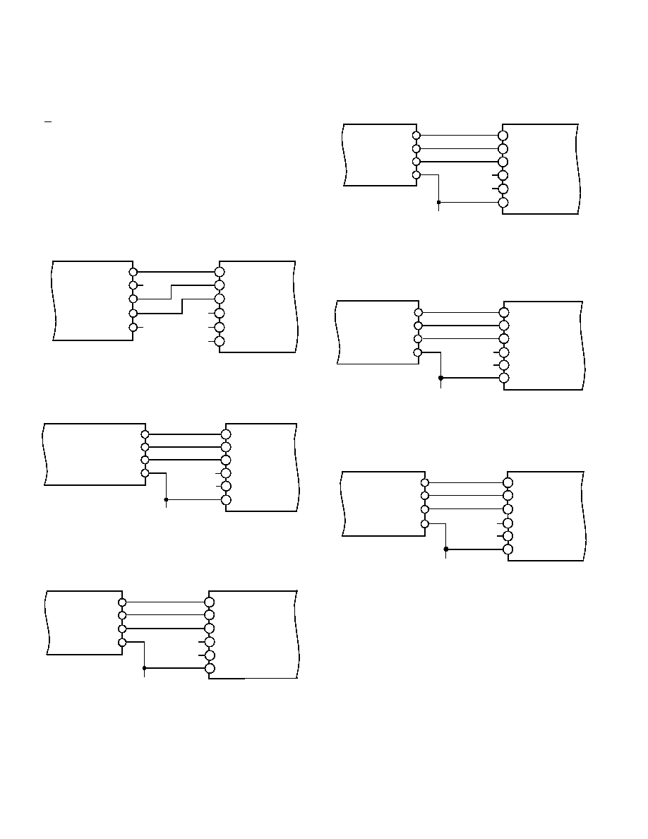
Figure 18 shows the suggested interface to the Philips SAA2500*
MPEG audio decoder IC. The SAA2500 supports 18 bits of
data using an I
2
S-compatible output format.
SCK
WS
FSCLKIN
SD
SAA2500
256 x Fs
HI
L
R
CLK
BCLK
SDATA
MODE
AD1857
384/
256
20
19
18
3
6
MCLK
1
HI
Figure 18. Interface to SAA2500
Figure 19 shows the suggested interface to the Zoran ZR38000*
DSP chip, which can act as an MPEG audio or AC-3 audio
decoder. The ZR38000 supports 16 bits of data using a left-
justified output format.
20
SCKB
WSB
SCKIN
SDB
ZR38000
256 x Fs
LO
L
R
CLK
BCLK
SDATA
MODE
AD1857
384/
256
19
18
3
6
MCLK
1
HI
Figure 19. Interface to ZR38000
Figure 20 shows the suggested interface to the C-Cube
Microsystems CL480* MPEG system decoder IC. The CL480
supports 16 bits of data using a right-justified output format.
20
19
18
DA-BCK
DA-LRCK
DA-XCK
DA-DATA
CL480
256 x Fs
HI
L
R
CLK
BCLK
SDATA
MODE
AD1858
3
6
384/
256
HI
MCLK
1
Figure 20. Interface to CL480
Control Signals
The MODE and DEEMP control inputs are normally connected
HI or LO to establish the operating state of the AD1857/AD1858.
They can be changed dynamically (and asynchronously to the
L
RCLK and the master clock) as long as they are stable before
the first serial data input bit (i.e., the MSB) is presented to the
AD1857/AD1858.
APPLICATION ISSUES
Interface to MPEG Audio Decoders
Figure 15 shows the suggested interface to the Analog Devices
ADSP-21xx family of DSP chips, for which several MPEG
audio decode algorithms are available. The ADSP-21xx
supports 16 bits of data using a left-justified DSP serial port
style format.
SCLK
DR
RFS
TFS
DT
ADSP-21xx
NC
NC
HI
L
R
CLK
BCLK
SDATA
MODE
AD1858
384/
256
19
18
20
3
6
NC = NO CONNECT
HI
MCLK
1
Figure 15. Interface to ADSP-21xx
Figure 16 shows the suggested interface to the Texas Instruments
TMS320AV110* MPEG audio decoder IC. The TMS320AV110
supports 18 bits of data using a right-justified output format.
SCLK
LRCLK
PCMCLK
PCMDATA
TMS320AV110
256 x Fs
HI
L
R
CLK
BCLK
SDATA
MODE
AD1858
384/
256
18
19
20
3
6
MCLK
1
HI
Figure 16. Interface to TMS320AV110
Figure 17 shows the suggested interface to the LSI Logic
L64111* MPEG audio decoder IC. The L64111 supports 16
bits of data using a left-justified output format.
SCLKO
LRCLKO
SYSCLK
SERO
L64111
384 x Fs
LO
L
R
CLK
BCLK
SDATA
MODE
AD1857
384/
256
20
19
18
3
6
MCLK
1
LO
Figure 17. Interface to L64111
*All trademarks are properties of their respective holders.

AD1857/AD1858
REV. 0
≠13≠
14
13
12
11
17
16
15
20
19
18
10
9
8
1
2
3
4
7
6
5
DIGITAL
GROUND
PLANE
MCLK
DV
DD
SDATA
L
R
CLK
BCLK
PD
/
RST
MODE
NC
AV
DD
MUTE
DGND
DEEMP
384/
256
AV
DD
OUTL
AGND
CMOUT
FILT
AGND
OUTR
ANALOG
GROUND
PLANE
NC = NO CONNECT
FERRITE
BEAD
Figure 22. Recommended Ground Plane
Layout and Decoupling Considerations
The recommended decoupling, bypass and output circuits for
the AD1857/AD1858 are shown in Figure 21.
PCB and Ground Plane Recommendations
The AD1857/AD1858 ideally should be located above a split
ground plane, with the digital pins over the digital ground plane
and the analog pins over the analog ground plane. The split
should occur between Pins 6 and 7, and between Pins 14 and
15 as shown in Figure 22. The ground planes should be linked
with a ferrite bead. This ground plane strategy maximizes the
AD1857/AD1858's analog audio performance.
2.2
µ
F
RIGHT LINE
OUTPUT
LEFT LINE
OUTPUT
AV
DD
AGND
FILT
CMOUT
+5V
ANALOG
SDATA
BLCK
L
R
CLK
MODE
AGND
DV
DD
DGND
+5V
DIGITAL
OUTL
OUTR
MUTE
DEEMP
NC
PD
/
RST
BIAS VOLTAGE
FOR EXTERNAL
USE
+5V
ANALOG
AV
DD
NC = NO CONNECT
0.1
µ
F
4.7
µ
F
0.1
µ
F
4.7
µ
F
AD1857/AD1858
MCLK
256 MODE
384 MODE
SAMPLE RATE
12.288MHz
18.432MHz
48kHz
44.1kHz
32kHz
11.2896MHz
16.9344MHz
8.192MHz
12.288MHz
384/
256
MCLK FREQUENCY
384/
256
= LO
384/
256
= HI
DSP OR
AUDIO
DECODER
0.1
µ
F
2.2
µ
F
µ
CONTROLLER
4.7
µ
F
0.01
µ
F
12
11
8
13
10
9
7
14
1
6
18
19
3
20
16
2
15
5
4
17
4.7
µ
F
RIGHT LINE
OUTPUT
LEFT LINE
OUTPUT
OUTL
OUTR
2.2
µ
F
8
13
100k
820pF
1k
+
2.2
µ
F
100k
820pF
1k
+
*OPTIONAL OUTPUT FILTER
*
*
Figure 21. Recommended Circuit Connection

AD1857/AD1858
REV. 0
≠14≠
BCLK
L
R
CLK
SDATA
LEFT-JUSTIFIED
MODE
AD1857
SDATA
RIGHT-JUSTIFIED
MODE
AD1858
LSB
SDATA
I
2
S-JUSTIFIED
MODE
AD1857
t
DBH
t
DBP
t
DBL
t
DLS
t
DDS
MSB
MSB-1
t
DDH
t
DDS
MSB
t
DDH
t
DDS
t
DDS
t
DDH
t
DDH
MSB
Figure 23. Serial Data Port Timing
BCLK
L
R
CLK
SDATA
LEFT-JUSTIFIED
DSP SERIAL
PORT STYLE MODE
AD1858
MSB-1
t
DBH
t
DBP
t
DBL
t
DLS
t
DLH
t
DDS
t
DDH
MSB
Figure 24. Serial Data Port Timing≠DSP Serial Port Style Mode (AD1858 Only)
PD
/
RST
MCLK
t
PDRP
Figure 25. Power-Down/Reset Timing
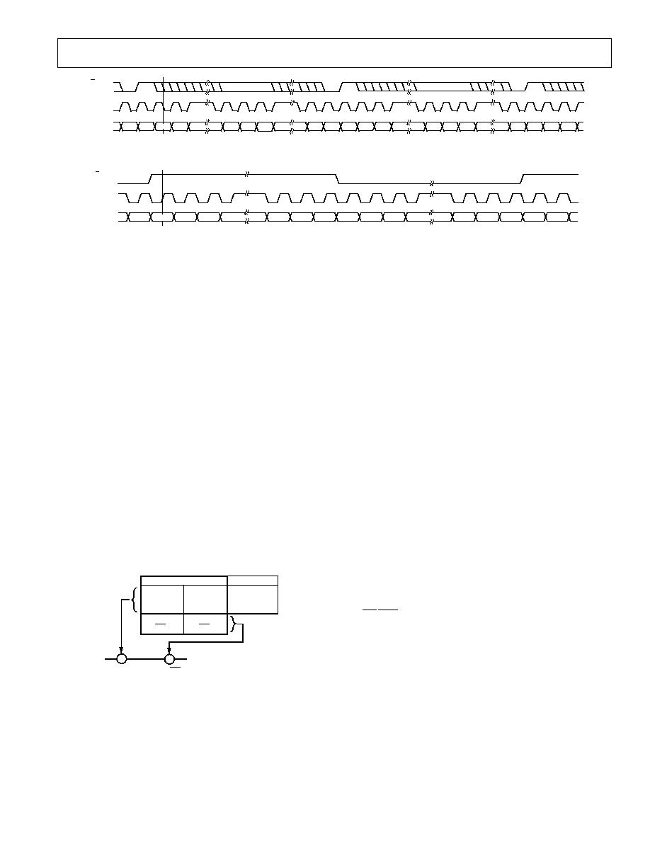
Timing Diagrams
The serial data port timing is shown in Figures 23 and 24. The
minimum bit clock HI pulse width is t
DBH
and the minimum bit
clock LO pulse width is t
DBL
. The minimum bit clock period is
t
DBP
. The left/
right clock minimum setup time is t
DLS
and the
left/
right clock minimum hold time is t
DLH
. The serial data
minimum setup time is t
DDS
and the minimum serial data hold
time is t
DDH
.
The power-down/reset timing is shown in Figure 25. The
minimum reset LO pulse width is t
PDRP
(four MCLK periods)
to accomplish a successful AD1857/AD1858 reset operation.

AD1857/AD1858
REV. 0
≠15≠
OUTLINE DIMENSIONS
Dimensions shown in inches and (mm).
20-Lead SSOP
(RS-20)
20
11
10
1
0.295 (7.50)
0.271 (6.90)
0.311 (7.9)
0.301 (7.64)
0.212 (5.38)
0.205 (5.207)
PIN 1
SEATING
PLANE
0.008 (0.203)
0.002 (0.050)
0.07 (1.78)
0.066 (1.67)
0.0256
(0.65)
BSC
0.078 (1.98)
0.068 (1.73)
0.009 (0.229)
0.005 (0.127)
0.037 (0.94)
0.022 (0.559)
8
∞
0
∞
1. LEAD NO. 1 IDENTIFIED BY A DOT.
2. LEADS WILL BE EITHER TIN PLATED OR SOLDER DIPPED
IN ACCORDANCE WITH MIL-M-38510 REQUIREMENTS

C2218≠12≠4/97
PRINTED IN U.S.A.
≠16≠