 | –≠–ª–µ–∫—Ç—Ä–æ–Ω–Ω—ã–π –∫–æ–º–ø–æ–Ω–µ–Ω—Ç: AD1859 | –°–∫–∞—á–∞—Ç—å:  PDF PDF  ZIP ZIP |

a
Stereo, Single-Supply
18-Bit Integrated
DAC
AD1859
PRODUCT OVERVIEW
The AD1859 is a complete 16-/18-bit single-chip stereo digital
audio playback subsystem. It comprises a variable rate
digital
interpolation filter, a revolutionary multibit sigma-delta (
)
modulator with dither, a jitter-tolerant DAC, switched capacitor
and continuous time analog filters, and analog output drive cir-
cuitry. Other features include an on-chip stereo attenuator and
mute, programmed through an SPI-compatible serial control
port.
The key differentiating feature of the AD1859 is its asynchro-
nous master clock capability. Previous
audio DACs re-
quired a high frequency master clock at 256 or 384 times the
intended audio sample rate. The generation and management
of this high frequency synchronous clock is burdensome to the
board level designer. The analog performance of conventional
single bit
DACs is also dependent on the spectral purity of
the sample and master clocks. The AD1859 has a digital Phase
Locked Loop (PLL) which allows the master clock to be asyn-
chronous, and which also strongly rejects jitter on the sample
clock (left/right clock). The digital PLL allows the AD1859 to
be clocked with a single frequency (27 MHz for example) while
the sample frequency (as determined from the left/right clock)
can vary over a wide range. The digital PLL will lock to the
new sample rate in approximately 100 ms. Jitter components
15 Hz above and below the sample frequency are rejected by
6 dB per octave. This level of jitter rejection is unprecedented
in audio DACs.
The AD1859 supports continuously variable sample rates with
essentially linear phase response, and with an option for external
analog de-emphasis processing. The clock circuit includes an
on-chip oscillator, so that the user need only provide an external
crystal. The oscillator may be overdriven, if desired, with an ex-
ternal clock source.
(continued on page 7)
*SPI is a registered trademark of Motorola, Inc.
REV. A
Information furnished by Analog Devices is believed to be accurate and
reliable. However, no responsibility is assumed by Analog Devices for its
use, nor for any infringements of patents or other rights of third parties
which may result from its use. No license is granted by implication or
otherwise under any patent or patent rights of Analog Devices.
© Analog Devices, Inc., 1996
One Technology Way, P.O. Box 9106, Norwood. MA 02062-9106, U.S.A.
Tel: 617/329-4700
Fax: 617/326-8703
FEATURES
Complete, Low Cost Stereo DAC System in a Single Die
Package
Variable Rate Oversampling Interpolation Filter
Multibit
Modulator with Triangular PDF Dither
Discrete and Continuous Time Analog Reconstruction
Filters
Extremely Low Out-of-Band Energy
64 Step (1 dB/Step) Analog Attenuator with Mute
Buffered Outputs with 2 k Output Load Drive
Rejects Sample Clock Jitter
94 dB Dynamic Range, ≠88 dB THD+N Performance
Option for Analog De-emphasis Processing with
External Passive Components
0.1 Maximum Phase Linearity Deviation
Continuously Variable Sample Rate Support
Digital Phase Locked Loop Based Asynchronous Master
Clock
On-Chip Master Clock Oscillator, Only External Crystal
Is Required
Power-Down Mode
Flexible Serial Data Port (I
2
S-Justified, Left-Justified,
Right-Justified and DSP Serial Port Modes)
SPI* Compatible Serial Control Port
Single +5 V Supply
28-Pin SOIC and SSOP Packages
APPLICATIONS
Digital Cable TV and Direct Broadcast Satellite Set-Top
Decoder Boxes
Digital Video Disc, Video CD and CD-I Players
High Definition Televisions, Digital Audio Broadcast
Receivers
CD, CD-R, DAT, DCC, ATAPI CD-ROM and MD Players
Digital Audio Workstations, Computer Multimedia
Products
FUNCTIONAL BLOCK DIAGRAM
SERIAL
CONTROL
INTERFACE
AD1859
16- OR 18-BIT
DIGITAL DATA
INPUT
6
ASYNCHRONOUS
CLOCK/CRYSTAL
DE-EMPHASIS
SWITCH LEFT
COMMON MODE
ANALOG
OUTPUTS
DE-EMPHASIS
SWITCH RIGHT
DE-EMPHASIS
MUTE
ANALOG
SUPPLY
2
REFERENCE
FILTER AND
GROUND
CONTROL
DATA
INPUT
2
3
2
DIGITAL
SUPPLY
POWER
DOWN/RESET
ATTEN/
MUTE
OUTPUT
BUFFER
DAC
VOLTAGE
REFERENCE
MULTIBIT
MODULATOR
VARIABLE RATE
INTERPOLATION
SERIAL
DATA
INTERFACE
ATTEN/
MUTE
OUTPUT
BUFFER
ANALOG
FILTER
DAC
MULTIBIT
MODULATOR
VARIABLE RATE
INTERPOLATION
DPLL/CLOCK
MANAGER
ANALOG
FILTER

TEST CONDITIONS UNLESS OTHERWISE NOTED
Supply Voltages (AV
DD
, DV
DD
)
+5.0
V
Ambient Temperature
25
∞
C
Input Clock (F
MCLK
)
27.1656
MHz
Input Signal
1001.2938 Hz
≠0.5
dB Full Scale
Input Sample Rate
44.1
kHz
Measurement Bandwidth
10 Hz to 20 kHz
Input Data Word Width
18
Bits
Load Capacitance
100
pF
Input Voltage HI (V
IH
)
2.4
V
Input Voltage LO (V
IL
)
0.8
V
NOTES
I
2
S-Justified Mode (Ref. Figure 3).
Device Under Test (DUT) is bypassed, decoupled and dc-coupled as shown in Figure 17 (no de-emphasis circuit).
Performance of the right and left channels are identical (exclusive of "Interchannel Gain Mismatch" and "Interchannel Phase Deviation" specifications).
Attenuation setting is 0 dB.
Values in bold typeface are tested; all others are guaranteed, not tested.
ANALOG PERFORMANCE
Min
Typ
Max
Units
Resolution
18
Bits
Dynamic Range (20 to 20 kHz, ≠60 dB Input)
(No A-Weight Filter)
85.7
91
dB
(With A-Weight Filter)
88
94
dB
Total Harmonic Distortion + Noise
≠88
≠84
dB
0.004
0.0063
%
Analog Outputs
Single-Ended Output Range (
±
Full Scale)
2.8
3.0
3.2
V p-p
Output Impedance at Each Output Pin
17
24
Output Capacitance at Each Output Pin
20
pF
External Load Impedance (THD +N
≠84 dB)
750
2K
Out-of-Band Energy (0.5
◊
F
S
to 100 kHz)
≠72.5
dB
CMOUT
2.05
2.25
2.45
V
DC Accuracy
Gain Error
±
1
5
%
Interchannel Gain Mismatch
0.01
0.225
dB
Gain Drift
140
270
ppm/
∞
C
Interchannel Crosstalk (EIAJ Method)
101
dB
Interchannel Phase Deviation
±
0.1
Degrees
Attenuator Step Size
0.6
1.0
1.4
dB
Attenuator Range Span
≠61.5
≠62.5
≠63.5
dB
Mute Attenuation
≠70
≠74.2
dB
De-Emphasis Switch (EMPL, EMPR) DC Resistance
3
10
50
DIGITAL INPUTS
Min
Typ
Max
Units
Input Voltage HI (V
IH
)
2.4
V
Input Voltage LO (V
IL
)
0.8
V
Input Leakage (I
IH
@ V
IH
= 2.4 V)
1
6
µ
A
Input Leakage (I
IL
@ V
IL
= 0.8 V)
1
6
µ
A
Input Capacitance
20
pF
REV. A
≠2≠
AD1859≠SPECIFICATIONS

DIGITAL TIMING (Guaranteed over ≠40
∞
C to +105
∞
C, AV
DD
= DV
DD
= +5.0 V
±
10%)
Min
Typ
Max
Units
t
DBH
BCLK HI Pulse Width
25
ns
t
DBL
BCLK LO Pulse Width
25
ns
t
DBP
BCLK Period
50
ns
t
DLS
LRCLK Setup
5
ns
t
DLH
LRCLK Hold (DSP Serial Port Style Mode Only)
0
ns
t
DDS
SDATA Setup
0
ns
t
DDH
SDATA Hold
5
ns
t
CCH
CCLK HI Pulse Width
15
ns
t
CCL
CCLK LO Pulse Width
15
ns
t
CCP
CCLK Period
30
ns
t
CSU
CDATA Setup
0
ns
t
CHD
CDATA Hold
5
ns
t
CLD
CLATCH Delay
15
ns
t
CLL
CLATCH LO Pulse Width
5
ns
t
CLH
CLATCH HI Pulse Width
10
ns
t
PDRP
PD/RST
LO Pulse Width
4 MCLK Periods
(
150 ns @ 27 MHz)
t
MCP
MCLK Period
30
37
60
ns
F
MC
MCLK Frequency (1/t
MCP
)
17
27
33
MHz
t
MCH
MCLK HI Pulse Width
15
ns
t
MCL
MCLK LO Pulse Width
15
ns
POWER
Min
Typ
Max
Units
Supplies
Voltage, Analog and Digital
4.5
5
5.5
V
Analog Current
29.5
36
mA
Analog Current--Power Down
0.5
15
µ
A
Digital Current
23.5
30
mA
Digital Current--Power Down
6
9.5
mA
Dissipation
Operation--Both Supplies
265
330
mW
Operation--Analog Supply
147.5
180
mW
Operation--Digital Supply
117.5
150
mW
Power Down--Both Supplies
30
48
mW
Power Supply Rejection Ratio
1 kHz 300 mV p-p Signal at Analog Supply Pins
55
dB
20 kHz 300 mV p-p Signal at Analog Supply Pins
52
dB
TEMPERATURE RANGE
Min
Typ
Max
Units
Specifications Guaranteed
25
∞
C
Functionality Guaranteed
≠40
+105
∞
C
Storage
≠55
+125
∞
C
PACKAGE CHARACTERISTICS
Typ
Units
SOIC
JA
(Thermal Resistance [Junction-to-Ambient])
120.67
∞
C/W
SOIC
JC
(Thermal Resistance [Junction-to-Case])
13.29
∞
C/W
SSOP
JA
(Thermal Resistance [Junction-to-Ambient])
190.87
∞
C/W
SSOP
JC
(Thermal Resistance [Junction-to-Case])
15.52
∞
C/W
AD1859
REV. A
≠3≠

REV. A
≠4≠
AD1859
ABSOLUTE MAXIMUM RATINGS*
Min
Typ
Max
Units
DV
DD
to DGND
≠0.3
6
V
AV
DD
to AGND
≠0.3
6
V
Digital Inputs
DGND ≠ 0.3
DV
DD
+ 0.3
V
Analog Inputs
AGND ≠ 0.3
AV
DD
+ 0.3
V
AGND to DGND
≠0.3
0.3
V
Reference Voltage
Indefinite Short Circuit to Ground
Soldering
+300
∞
C
10
sec
*Stresses greater than those listed under "Absolute Maximum Ratings" may cause permanent damage to the device. This is a stress rating only and functional operation
of the device at these or any other conditions above those indicated in the operational section of this specification is not implied. Exposure to absolute maximum rating
conditions for extended periods may affect device reliability.
DIGITAL FILTER CHARACTERISTICS
Min
Typ
Max
Units
Passband Ripple
±
0.045
dB
Stopband
1
Attenuation
62
dB
48 kHz F
S
Passband
0
21.312
kHz
Stopband
26.688
6117
kHz
44.1 kHz F
S
Passband
0
19.580
kHz
Stopband
24.520
5620
kHz
32 kHz F
S
Passband
0
14.208
kHz
Stopband
17.792
4078
kHz
Other F
S
Passband
0
0.444
F
S
Stopband
0.556
127.444
F
S
Group Delay
40/F
S
sec
Group Delay Variation
0
µ
s
ANALOG FILTER CHARACTERISTICS
Min
Typ
Max
Units
Passband Ripple
≠0.075
dB
Stopband Attenuation (at 64
◊
F
S
)
58
dB
NOTE
1
Stopband nominally repeats itself at multiples of 128
◊
F
S
, where F
S
is the input word rate. Thus the digital filter will attenuate to 62 dB across the frequency
spectrum except for a range
±
0.55
◊
F
S
wide at multiples of 128
◊
F
S
.
WARNING!
ESD SENSITIVE DEVICE
CAUTION
ESD (electrostatic discharge) sensitive device. Electrostatic charges as high as 4000 V readily
accumulate on the human body and test equipment and can discharge without detection.
Although the AD1859 features proprietary ESD protection circuitry, permanent damage may
occur on devices subjected to high energy electrostatic discharges. Therefore, proper ESD
precautions are recommended to avoid performance degradation or loss of functionality.
ORDERING GUIDE
Temperature
Package
Package
Model
Range
Description
Option
AD1859JR
≠40
∞
C to +105
∞
C
28-Lead SOIC
R-28
AD1859JRS
≠40
∞
C to +105
∞
C
28-Lead SSOP
RS-28
PIN CONNECTIONS
NC = NO CONNECT
CMOUT
DEEMP
FILT
FGND
NC
EMPL
OUTL
AGND
MUTE
NC
AV
DD
NC
EMPR
OUTR
18/
16
CLATCH
IDPM0
CDATA
IDPM1
CCLK
DGND
SDATA
DV
DD
L
R
CLK
XTALI/MCLK
BCLK
XTALO
13
18
1
2
28
27
5
6
7
24
23
22
3
4
26
25
8
21
9
20
10
19
11
12
17
16
14
15
TOP VIEW
(Not to Scale)
AD1859
PD/RST
AD1859
REV. A
≠5≠
Serial Control Port Interface
Pin Name Number
I/O
Description
CDATA
20
I
Serial control input, MSB first,
containing 8 bits of unsigned
data per channel. Used for
specifying channel specific
attenuation and mute.
CCLK
19
I
Control clock input for control
data. Control input data must
be valid on the rising edge of
CCLK. CCLK may be continu-
ous or gated.
CLATCH
21
I
Latch input for control data. This
input is rising edge sensitive.
Digital Audio Serial Input Interface
Pin Name Number
I/O
Description
SDATA
12
I
Serial input, MSB first, contain-
ing two channels of 16 or 18 bits
of twos complement data per
channel.
BCLK
14
I
Bit clock input for input data.
Need not run continuously; may
be gated or used in a burst
fashion.
LRCLK
13
I
Left/right clock input for input
data. Must run continuously.
IDPM0
9
I
Input serial data port mode
control zero. With IDPM1,
defines one of four serial input
modes.
IDPM1
10
I
Input serial data port mode con-
trol one. With IDPM0, defines
one of four serial input modes.
18/16
8
I
18-bit or 16-bit input data mode
control. Connect this signal HI
for 18-bit input mode, LO for
16-bit input mode.
Gain Error
With a near full-scale input, the ratio of actual output to ex-
pected output, expressed as a percentage.
Interchannel Gain Mismatch
With identical near full-scale inputs, the ratio of outputs of the
two stereo channels, expressed in decibels.
Gain Drift
Change in response to a near full-scale input with a change in
temperature, expressed as parts-per-million (ppm) per
∞
C.
Crosstalk (EIAJ method)
Ratio of response on one channel with a zero input to a full-scale
1 kHz sine-wave input on the other channel, expressed in decibels.
Interchannel Phase Deviation
Difference in output sampling times between stereo channels,
expressed as a phase difference in degrees between 1 kHz inputs.
Power Supply Rejection
With zero input, signal present at the output when a 300 mV
p-p signal is applied to power supply pins, expressed in decibels
of full scale.
Group Delay
Intuitively, the time interval required for an input pulse to ap-
pear at the converter's output, expressed in seconds (s). More
precisely, the derivative of radian phase with respect to radian
frequency at a given frequency.
Group Delay Variation
The difference in group delays at different input frequencies.
Specified as the difference between the largest and the smallest
group delays in the passband, expressed in microseconds (
µ
s).
DEFINITIONS
Dynamic Range
The ratio of a full-scale output signal to the integrated output
noise in the passband (0 to 20 kHz), expressed in decibels (dB).
Dynamic range is measured with a ≠60 dB input signal and is
equal to (S/[THD+N]) + 60 dB. Note that spurious harmonics
are below the noise with a ≠60 dB input, so the noise level es-
tablishes the dynamic range. This measurement technique is
consistent with the recommendations of the Audio Engineering
Society (AES17-1991) and the Electronics Industries Association
of Japan (EIAJ CP-307).
Total Harmonic Distortion + Noise (THD+N)
The ratio of the root-mean-square (rms) value of a full-scale
fundamental input signal to the rms sum of all other spectral
components in the passband, expressed in decibels (dB) and
percentage.
Passband
The region of the frequency spectrum unaffected by the attenu-
ation of the digital interpolation filter.
Passband Ripple
The peak-to-peak variation in amplitude response from equal-
amplitude input signal frequencies within the passband, ex-
pressed in decibels.
Stopband
The region of the frequency spectrum attenuated by the digi-
tal interpolation filter to the degree specified by "stopband
attenuation."
PIN DESCRIPTIONS

REV. A
≠6≠
AD1859
Analog Signals
Pin Name
Number
I/O
Description
FILT
28
O
Voltage reference filter capacitor
connection. Bypass and decouple
the voltage reference with paral-
lel 10
µ
F and 0.1
µ
F capacitors
to the FGND pin.
FGND
27
I
Voltage reference filter ground.
Use exclusively for bypassing and
decoupling of the FILT pin
(voltage reference).
CMOUT
1
O
Voltage reference common-mode
output. Should be decoupled
with 10
µ
F capacitor to the AGND
pin or plane. This output is available
externally for dc-coupling and level-
shifting. CMOUT should not have
any signal dependent load, or where
it will sink or source current.
OUTL
4
O
Left channel line level analog output.
OUTR
25
O
Right channel line level analog output.
EMPL
3
O
De-emphasis switch connection
for the left channel. Can be left
unconnected if de-emphasis is not
required in the target application.
EMPR
26
O
De-emphasis switch connection
for the right channel. Can be left
unconnected if de-emphasis is not
required in the target application.
Control and Clock Signals
Pin Name
Number
I/O
Description
PD/RST
11
I
Power down/reset. The AD1859 is
placed in a low power consumption
"sleep" mode when this pin is held
LO. The AD1859 is reset on the
rising edge of this signal. The serial
control port registers are reset to
their default values. Connect HI
for normal operation.
DEEMP
2
I
De-emphasis. An external analog de-
emphasis circuit network is enabled
when this input signal is HI. This
circuit is typically used to impose a
50/15
µ
s (or perhaps the CCITT
J.17) response characteristic on the
output audio spectrum.
MUTE
7
I
Mute. Assert HI to mute both
stereo analog outputs of the AD1859.
Deassert LO for normal operation.
XTALI/
MCLK
16
I
Crystal input or master clock input.
Connect to one side of a quartz
crystal to this input, or connect to
an external clock source to over-
drive the on-chip oscillator.
XTALO
15
O
Crystal output. Connect to other
side of a quartz crystal. Do not con-
nect if using the XTALI/MCLK
pin with an external clock source.
Power Supply Connections and Miscellaneous
Pin Name
Number
I/O
Description
AV
DD
23
I
Analog Power Supply. Connect
to analog +5 V supply.
AGND
6
I
Analog Ground.
DV
DD
17
I
Digital Power Supply. Connect
to digital +5 V supply.
DGND
18
I
Digital Ground.
NC
5, 22, 24
No Connect. Reserved. Do not
connect.
PIN DESCRIPTIONS

AD1859
REV. A
≠7≠
(continued from page 1)
The AD1859 has a simple but very flexible serial data input port
that allows for glueless interconnection to a variety of ADCs,
DSP chips, AES/EBU receivers and sample rate converters.
The serial data input port can be configured in left-justified,
I
2
S-justified, right-justified and DSP serial port compatible
modes. The AD1859 accepts 16- or 18-bit serial audio data in
MSB-first, twos-complement format. A power-down mode is
offered to minimize power consumption when the device is inac-
tive. The AD1859 operates from a single +5 V power supply. It
is fabricated on a single monolithic integrated circuit using a
0.6
µ
M CMOS double polysilicon, double metal process, and is
housed in 28-pin SOIC and SSOP packages for operation over
the temperature range ≠40
∞
C to +105
∞
C.
THEORY OF OPERATION
The AD1859 offers the advantages of sigma-delta conversion
architectures (no component trims, low cost CMOS process
technology, superb low level linearity performance) with the
advantages of conventional multibit R-2R resistive ladder audio
DACs (no requirement for any high frequency synchronous master
clocks [e.g., 256 or 384
◊
F
S
] continuously variable sample rate
support, jitter tolerance, low output noise, etc.).
The use of a multibit sigma-delta modulator means that the
AD1859 generates dramatically lower amounts of out-of-band
noise energy, which greatly reduces the requirement on post
DAC filtering. The required post-filtering is integrated on the
AD1859. The AD1859's multibit sigma-delta modulator is also
highly immune to digital substrate noise.
The digital phase locked loop feature gives the AD1859 an un-
precedented jitter rejection feature. The bandwidth of the first
order loop filter is 15 Hz; jitter components on the input
left/right clock are attenuated by 6 dB per octave above and be-
low 15 Hz. Jitter on the crystal time base or MCLK input is re-
jected as well (by virtue of the on-chip switched capacitor filter),
but this clock should be low jitter because it is used by the DAC
to convert the audio from the discrete time (sampled) domain to
the continuous time (analog) domain. The AD1859 includes an
on-chip oscillator, so that the user need only provide an inexpen-
sive quartz crystal or ceramic resonator as an external time base.
Serial Audio Data Interface
The serial audio data interface uses the bit clock (BCLK) simply
to clock the data into the AD1859. The bit clock may, there-
fore, be asynchronous to the L/R clock. The left/right clock
(LRCLK) is both a framing signal, and the sample frequency input
to the digital phase locked loop. The left/right
clock (LRCLK) is
the signal that the AD1859 actually uses to determine the input
sample rate, and it is the jitter on LRCLK that is rejected by the
digital phase locked loop. The SDATA input carries the serial
stereo digital audio in MSB first, twos-complement format.
Digital Interpolation Filter
The purpose of the interpolator is to "oversample" the input
data, i.e., to increase the sample rate so that the attenuation re-
quirements on the analog reconstruction filter are relaxed. The
AD1859 interpolator increases the input data sample rate by a
variable factor depending on the sample frequency of the incom-
ing digital audio. The interpolation is performed using a multi-
stage FIR digital filter structure. The first stage is a droop
equalizer; the second and third stages are half-band filters; and
the fourth stage is a second-order comb filter. The FIR filter
implementation is multiplier-free, i.e., the multiplies are per-
formed using shift-and-add operations.
Multibit Sigma-Delta Modulator
The AD1859 employs a four-bit sigma-delta modulator. Whereas a
traditional single bit sigma-delta modulator has two levels of quan-
tization, the AD1859's has 17 levels of quantization. Traditional
single bit sigma-delta modulators sample the input signal at 64
times the input sample rate; the AD1859 samples the input sig-
nal at nominally 128 times the input sample rate. The addi-
tional quantization levels combined with the higher oversampling
ratio means that the AD1859 DAC output spectrum contains
dramatically lower levels of out-of-band noise energy, which is a
major stumbling block with more traditional single bit sigma-
delta architectures. This means that the post-DAC analog re-
construction filter has reduced transition band steepness and
attenuation requirements, which equates directly to lower phase
distortion. Since the analog filtering generally establishes the
noise and distortion characteristic of the DAC, the reduced
requirements translate into better audio performance.
Multibit sigma-delta modulators bring an additional benefit:
they are essentially free of stability (and therefore potential loop
oscillation) problems. They are able to use a wider range of the
voltage reference, which can increase the overall dynamic range
of the converter.
The conventional problem which limits the performance of
multibit sigma delta converters is the nonlinearity of the passive
circuit elements used to sum the quantization levels. Analog
Devices has developed (and been granted patents on) a revolu-
tionary architecture which overcomes the component linearity
problem that otherwise limits the performance of multibit sigma
delta audio converters. This new architecture provides the
AD1859 with the same excellent differential nonlinearity and
linearity drift (over temperature and time) specifications as
single bit sigma-delta DACs.
The AD1859's multibit modulator has another important ad-
vantage; it has a high immunity to substrate digital noise. Sub-
strate noise can be a significant problem in mixed-signal
designs, where it can produce intermodulation products that
fold down into the audio band. The AD1859 is approximately
eight times less sensitive to digital substrate noise (voltage refer-
ence noise injection) than equivalent single bit sigma-delta
modulator based DACs.
Dither Generator
The AD1859 includes an on-chip dither generator, which is in-
tended to further reduce the quantization noise introduced by
the multibit DAC. The dither has a triangular Probability Dis-
tribution Function (PDF) characteristic, which is generally con-
sidered to create the most favorable noise shaping of the residual
quantization noise. The AD1859 is among the first low cost, IC
audio DACs to include dithering.
Analog Filtering
The AD1859 includes a second-order switched capacitor dis-
crete time low-pass filter followed by a first-order analog con-
tinuous time low-pass filter. These filters eliminate the need for
any additional off-chip external reconstruction filtering. This
on-chip switched capacitor analog filtering is essential to reduce
the deleterious effects of any remaining master clock jitter.

REV. A
≠8≠
AD1859
Option for Analog De-emphasis Processing
The AD1859 includes three pins for implementing an external
analog 50/15
µ
s (or possibly the CCITT J. 17) de-emphasis fre-
quency response characteristic. A control pin DEEMP (Pin 2)
enables de-emphasis when it is asserted HI. Two analog out-
puts, EMPL (Pin 3) and EMPR (Pin 26) are used to switch the
required analog components into the output stage of the AD1859.
An analog implementation of de-emphasis is superior to a digital
implementation in several ways. It is generally lower noise, since
digital de-emphasis is usually created using recursive IIR filters,
which inject limit cycle noise. Also the digital de-emphasis is be-
ing applied in front of the primary analog noise generation source,
the DAC modulator, and its high frequency noise contributions
are not attenuated. An analog de-emphasis circuit is down-
stream from the relatively "noisy" DAC modulator and thus pro-
vides a more effective noise reduction role (which was the original
intent of the emphasis/de-emphasis scheme). A final key advan-
tage of analog de-emphasis is that it is sample rate invariant, so
that users can fully exploit the sample rate range of the AD1859
and simultaneously use de-emphasis. Digital implementations gen-
erally only support fixed, standard sample rates.
Digital Phase Locked Loop
The digital PLL is adaptive, and locks to the applied sample rate
(on the LRCLK Pin 13) in 100 ms to 200 ms. The digital PLL
is initially in "fast" mode, with a wide lock capture bandwidth.
The phase detector automatically switches the loop filter into
"slow" mode as phase lock is gradually obtained. The loop
bandwidth is 15 Hz in slow mode. Since the loop filter is first
order, the digital PLL will reject jitter on the left/right clock
above 15 Hz, with an attenuation of 6 dB per octave. The jitter
rejection frequency response is shown in Figure 1.
≠60
≠42
≠54
15
≠48
0
≠24
≠36
≠30
≠18
≠12
≠6
0
15360
7680
3840
1920
960
480
240
120
60
30
JITTER ATTENUATION ≠ dB
Hz ABOVE OR BELOW THE SAMPLE FREQUENCY
Figure 1. Digital PLL Jitter Rejection
OPERATING FEATURES
Serial Data Input Port
The AD1859 uses the frequency of the left/right input clock to
determine the input sample rate. LRCLK must run continu-
ously and transition twice per stereo sample period (except in
the left-justified DSP serial port style mode, when it transitions
four times per stereo sample period). The bit clock (BCLK) is
edge sensitive and may be used in a gated or burst mode (i.e., a
stream of pulses during data transmission followed by periods of
inactivity). The bit clock is only used to write the audio data
into the serial input port. It is important that the left/right clock
is "clean" with monotonic rising and falling edge transitions and
no excessive overshoot or undershoot which could cause false
clock triggering of the AD1859.
The AD1859's flexible serial data input port accepts data in
twos-complement, MSB-first format. The left channel data
field always precedes the right channel data field. The input
data consists of either 16 or 18 bits, as established by the 18/16
input control (Pin 8). All digital inputs are specified to TTL
logic levels. The input data port is configured by control pins.
Serial Input Port Modes
The AD1859 uses two multiplexed input pins to control the
mode configuration of the input data port. IDPM0 and IDPM1
program the input data port mode as follows:
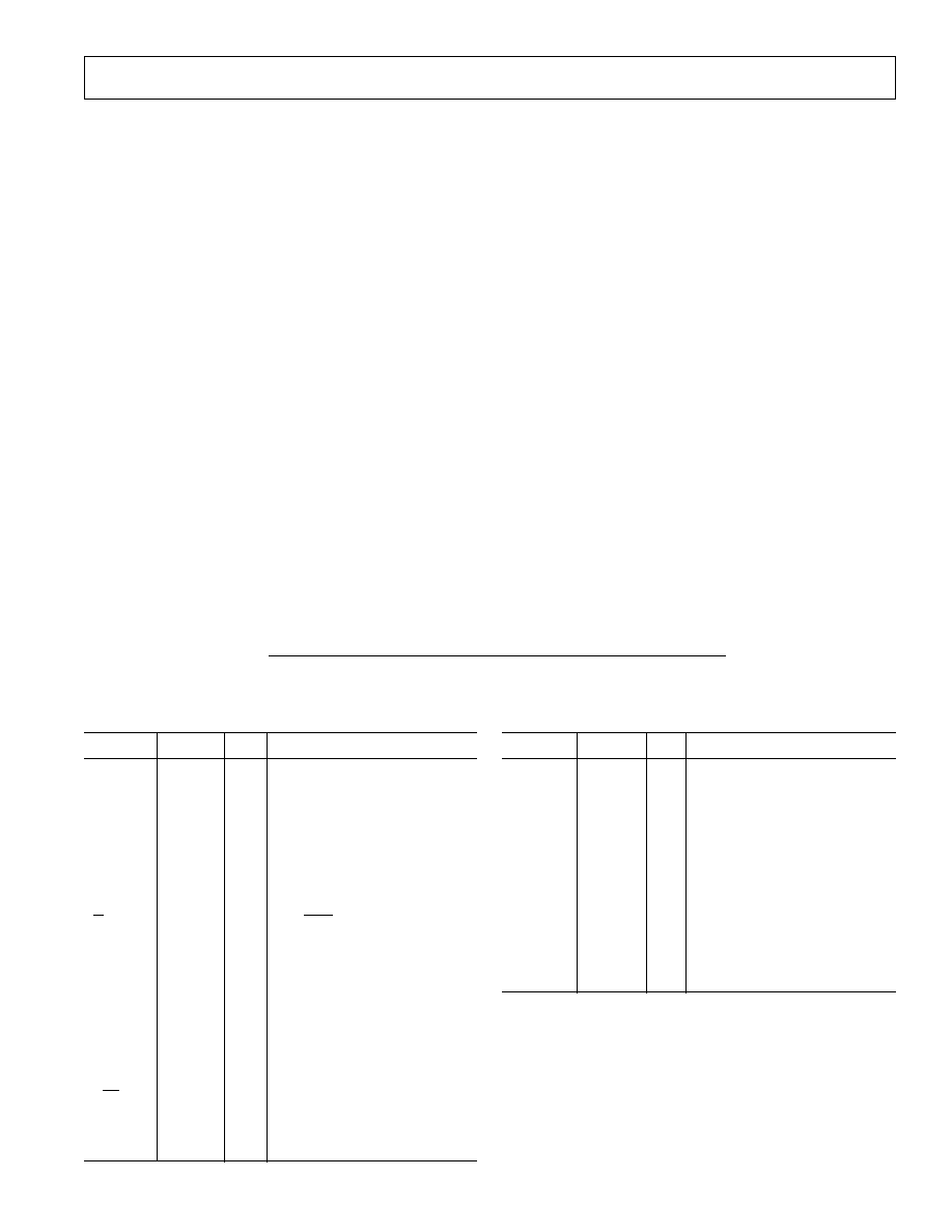
IDPM1
IDPM0
Serial Input Port Mode
LO
LO
Right-Justified (See Figure 2)
LO
HI
I
2
S-Justified (See Figure 3)
HI
LO
Left-Justified (See Figure 4)
HI
HI
Left-Justified DSP Serial Port Style
(See Figure 5)
Figure 2 shows the right-justified mode. LRCLK is HI for the
left channel, and LO for the right channel. Data is valid on the
rising edge of BCLK. The MSB is delayed 14-bit clock periods
(in 18-bit input mode) or 16-bit clock periods (in 16-bit input
mode) from an LRCLK transition, so that when there are 64
BCLK periods per LRCLK period, the LSB of the data will be
right-justified to the next LRCLK transition.
MSB-1
MSB-2
LSB+2
LSB+1
LSB
MSB
MSB-1
MSB-2
LSB
LSB+2
LSB+1
LSB
LEFT CHANNEL
RIGHT CHANNEL
MSB
BCLK
INPUT
SDATA
INPUT
LRCLK
INPUT
Figure 2. Right-Justified Mode

AD1859
REV. A
≠9≠
Figure 3 shows the I
2
S-justified mode. LRCLK is LO for the left
channel, and HI for the right channel. Data is valid on the rising
edge of BCLK. The MSB is left-justified to an LRCLK transition
but with a single BCLK period delay. The I
2
S-justified mode
can be used in either the 16-bit or the 18-bit input mode.
Figure 4 shows the left-justified mode. LRCLK is HI for the
left channel, and LO for the right channel. Data is valid on the
rising edge of BCLK. The MSB is left-justified to an LRCLK
transition, with no MSB delay. The left-justified mode can be
used in either the 16-bit or the 18-bit input mode.
Figure 5 shows the left-justified DSP serial port style mode.
LRCLK must pulse HI for at least one bit clock period before
the MSB of the left channel is valid, and LRCLK must pulse HI
again for at least one bit clock period before the MSB of the
right channel is valid. Data is valid on the falling edge of
BCLK. The left-justified DSP serial port style mode can be
used in either the 16-bit or the 18-bit input mode. Note that in
this mode, it is the responsibility of the DSP to ensure that the
left data is transmitted with the first LRCLK pulse, and that the
right data is transmitted with the second LRCLK pulse, and
that synchronism is maintained from that point forward.
Note that in 16-bit input mode, the AD1859 is capable of a 32
◊
F
S
BCLK frequency "packed mode" where the MSB is left-
justified to an LRCLK transition, and the LSB is right-justified
to an LRCLK transition. LRCLK is HI for the left channel,
and LO for the right channel. Data is valid on the rising edge of
BCLK. Packed mode can be used when the AD1859 is pro-
grammed in either right-justified or left-justified mode. Packed
mode is shown in Figure 6.
Serial Control Port
The AD1859 serial control port is SPI compatible. SPI
(Serial Peripheral Interface) is a serial port protocol popularized
by Motorola's family of microcomputer and microcontroller
products. The write-only serial control port gives the user ac-
cess to channel specific mute and attenuation. The AD1859
serial control port consists of three signals, control clock CCLK
(Pin 19), control data CDATA (Pin 20), and control latch
CLATCH (Pin 21). The control data input (CDATA) must be
valid on the control clock (CCLK) rising edge, and the control
clock (CCLK) must only make a LO to HI transition when
there is valid data. The control latch (CLATCH) must make a
LO to HI transition after the LSB has been clocked into the
AD1859, while the control clock (CCLK) is inactive. The tim-
ing relation between these signals is shown in Figure 7.
MSB-1
MSB-2
LSB+2
LSB+1
LSB
MSB
MSB-1
MSB-2
LSB
LSB+2
LSB+1
LEFT CHANNEL
RIGHT CHANNEL
MSB
MSB
BCLK
INPUT
SDATA
INPUT
LRCLK
INPUT
Figure 3. I
2
S-Justified Mode
MSB-1
MSB-2
LSB+2
LSB+1
LSB
MSB
MSB-1
MSB-2
LSB
LSB+2
LSB+1
LEFT CHANNEL
RIGHT CHANNEL
MSB
MSB-1
MSB
BCLK
INPUT
SDATA
INPUT
LRCLK
INPUT
Figure 4. Left-Justified Mode
BCLK
INPUT
SDATA
INPUT
MSB
MSB-1
LSB+2
LSB+1
LSB
MSB
MSB-1
LSB
LSB+2
LSB+1
LEFT CHANNEL
RIGHT CHANNEL
MSB
MSB-1
LRCLK
INPUT
Figure 5. Left-Justified DSP Serial Port Style Mode
BCLK
INPUT
SDATA
INPUT
MSB-1
MSB-2
LSB+2
LSB+1
LSB
MSB
MSB-1
MSB-2
LSB
LSB+2
LSB+1
MSB
MSB-1
LSB
LEFT CHANNEL
RIGHT CHANNEL
MSB
LRCLK
INPUT
Figure 6. 32
◊
F
S
Packed Mode
REV. A
≠10≠
AD1859
D6
CCLK
CDATA
CLATCH
D7
D6
D5
D4
D3
D2
D1
D0
D7
D5
MSB
LSB
MSB
Figure 7. Serial Control Port Timing
DATA6
Mute
DATA5
Atten5
DATA4
Atten4
DATA3
Atten3
DATA2
Atten2
DATA1
Atten1
DATA0
Atten0
Right Channel = HI
Left Channel = LO
Mute = HI
Normal = LO
00 0000 = 0.0dB
00 0001 = ≠1.0dB
00 0010 = ≠2.0dB
00 0011 = ≠3.0dB
00 0100 = ≠4.0dB
00 0101 = ≠5.0dB
00 0110 = ≠6.0dB
00 0111 = ≠7.0dB
00 1000 = ≠8.0dB
*
*
*
11 1101 = ≠61.0dB
11 1110 = ≠62.0dB
11 1111 = ≠63.0dB
LSB
MSB
DATA7
LEFT/RIGHT
Figure 8. Serial Control Bit Definitions
The serial control port is byte oriented. The data is MSB first,
and is unsigned. There is a control register for the left channel
and a control register for the right channel, as distinguished by
the MSB (DATA7). The bits are assigned as shown in Figure 8.
The left channel control register and the right channel control reg-
ister have identical power up and reset default settings. DATA6,
the Mute control bit, reset default state is LO, which is the nor-
mal (nonmuted) setting. DATA5:0, the Atten5 through Atten0
control bits, have a reset default value of 00 0000, which is an
attenuation of 0.0 dB (i.e., full scale, no attenuation). The intent
with these reset defaults is to enable AD1859 applications with-
out requiring the use of the serial control port. For those users
that do not use the serial control port, it is still possible to mute
the AD1859 output by using the external MUTE (Pin 7) signal.
It is recommended that the output be muted for approximately
1000 input sample periods during power-up or following any
radical sample rate change (>5%) to allow the digital phase
locked loop to settle.
Note that the serial control port timing is asynchronous to the
serial data input port timing. Changes made to the attenuator
level will be updated on the next edge of the LRCLK after the
CLATCH write pulse. The AD1859 has been designed to re-
solve the potential for metastability between the LRCLK edge
and the CLATCH write pulse rising edge. The attenuator set-
ting is guaranteed to be valid even if the LRCLK edge and the
CLATCH rising edge occur essentially simultaneously.
On-Chip Oscillator and Master Clock
The asynchronous master clock of the AD1859 can be supplied
by either an external clock source applied to XTALI/MCLK or
by connecting a crystal across the XTALI/MCLK and XTALO
pins, and using the on-chip oscillator. If a crystal is used, it
should be fundamental-mode and parallel-tuned. Figure 9
shows example connections.
The range of audio sample rates (as determined from the
LRCLK input) supported by the AD1859 is a function of the
master clock rate (i.e., the crystal frequency or external clock
source frequency) applied. The highest sample rate supported
can be computed as follows:
Highest Sample Rate = Master Clock Frequency
˜
512
The lowest sample rate supported can be computed as follows:
Lowest Sample Rate = Master Clock Frequency
˜
1024
27MHz
27MHz OSCILLATOR CONNECTION
XTALI/MCLK
XTALO
AD1859
NC
20-64pF
20-64pF
27MHz
27MHz CRYSTAL CONNECTION
XTALI/MCLK
XTALO
AD1859
Figure 9. Crystal and Oscillator Connections
Figure 10 illustrates these relations. As can be seen in Figure 10,
a 27 MHz MCLK or crystal frequency supports audio sample
rates from approximately 28 kHz to 52 kHz.
76
20
36
28
44
52
60
68
20
18
34
30
28
24
22
26
32
36
XTAL/MCLK FREQUENCY ≠ MHz
HIGHEST
L/R SAMPLE RATE
(MCLK/512)
LOWEST
L/R SAMPLE RATE
(MCLK/1024)
L/R
CLOCK SAMPLE FREQUENCY ≠ kHz
Figure 10. MCLK Frequency vs. L/R Clock Frequency
Mute and Attenuation
The AD1859 offers two methods of muting the analog output.
By asserting the MUTE (Pin 7) signal HI, both the left channel
and the right channel are muted. As an alternative, the user can
assert the mute bit in the serial control registers HI for indi-
vidual mute of either the left channel or the right channel. The

AD1859
REV. A
≠11≠
AD1859 has been designed to minimize pops and clicks when
muting and unmuting the device. The AD1859 includes a zero
crossing detector which attempts to implement attenuation
changes on waveform zero crossings only. If a zero crossing is
not found within 1024 input sample periods (approximately
23 ms at 44.1 kHz), the attenuation change is made regardless.
Output Drive, Buffering and Loading
The AD1859 analog output stage is able to drive a 2 k
load. If
lower impedance loads must be driven, an external buffer stage
such as the Analog Devices SSM2142 should be used. The
analog output is generally ac coupled with a 10
µ
F capacitor,
even if the optional de-emphasis circuit is not used, as shown in
Figure 17. It is possible to dc couple the AD1859 output into an
op amp stage using the CMOUT signal as a bias point.
On-Chip Voltage Reference
The AD1859 includes an on-chip voltage reference that estab-
lishes the output voltage range. The nominal value of this refer-
ence is +2.25 V which corresponds to a line output voltage
swing of 3 V p-p. The line output signal is centered around a
voltage established by the CMOUT (common mode) output
(Pin 1). The reference must be bypassed both on the FILT in-
put (Pin 28) with 10
µ
F and 0.1
µ
F capacitors, and on the
CMOUT output (Pin 1) with a 10
µ
F and 0.1
µ
F capacitors, as
shown in Figures 17 and 18. The FILT pin must use the
FGND ground, and the CMOUT pin must use the AGND
ground. The on-chip voltage reference may be overdriven with
an external reference source by applying this voltage to the
FILT pin. CMOUT and FILT must still be bypassed as shown
in Figures 17 and 18. An external reference can be useful to
calibrate multiple AD1859 DACs to the same gain. Reference
bypass capacitors larger than those suggested can be used to im-
prove the signal-to-noise performance of the AD1859.
Power Down and Reset
The PD/RST input (Pin 11) is used to control the power con-
sumed by the AD1859. When PD/RST is held LO, the AD1859
is placed in a low dissipation power-down state. When PD/RST
is brought HI, the AD1859 becomes ready for normal operation.
The master clock (XTALI/MCLK, Pin 16) must be running for
a successful reset or power-down operation to occur. The PD/RST
signal must be LO for a minimum of four master clock periods
(approximately 150 ns with a 27 MHz XTALI/MCLK
frequency).
When the PD/RST input (Pin 11) is asserted brought HI, the
AD1859 is reset. All registers in the AD1859 digital engine (se-
rial data port, interpolation filter and modulator) are zeroed, and
the amplifiers in the analog section are shorted during the reset
operation. The two registers in the serial control port are initial-
ized to their default values. The user should wait 100 ms after
bringing PD/RST HI before using the serial data input port and
the serial control input port in order for the digital phase locked
loop to re-acquire lock. The AD1859 has been designed to
minimize pops and clicks when entering and exiting the power-
down state.
Control Signals
The IDPM0, IDPM1, 18/16, and DEEMP control inputs are
normally connected HI or LO to establish the operating state of
the AD1859. They can be changed dynamically (and asynchro-
nously to the LRCLK and the master clock) as long as they are
stable before the first serial data input bit (i.e., the MSB) is pre-
sented to the AD1859.
APPLICATIONS ISSUES
Interface to MPEG Audio Decoders
Figure 11 shows the suggested interface to the Analog Devices
ADSP-21xx family of DSP chips, for which several MPEG
audio decode algorithms are available. The ADSP-21xx supports
16 bits of data using a left-justified DSP serial port style format.
ADSP-21xx
NC
NC
HI
AD1859
13
14
8
9
10
12
HI
LO
BCLK
L
R
CLK
SDATA
IDPM0
IDPM1
18/
16
SCLK
RFS
TFS
DR
DT
Figure 11. Interface to ADSP-21xx
Figure 12 shows the suggested interface to the Texas Instru-
ments TMS320AV110 MPEG audio decoder IC. The
TMS320AV110 supports 18 bits of data using a right-justified
output format.
LO
AD1859
13
14
8
9
10
12
LO
HI
BCLK
L
R
CLK
SDATA
IDPM0
IDPM1
18/
16
TEXAS
INSTRUMENTS
TMS320AV110
48 x F
S
TO
1536 x F
S
SCLK
LRCLK
PCMDATA
PCMCLK
Figure 12. Interface to TMS320AV110
Figure 13 shows the suggested interface to the LSI Logic L64111
MPEG audio decoder IC. The L64111 supports 16 bits of data
using a left-justified output format.
LSI LOGIC
L64111
384 x F
S
OR
512 x F
S
LO
AD1859
13
14
8
9
10
12
HI
LO
BCLK
L
R
CLK
SDATA
IDPM0
IDPM1
18/
16
SCLKO
LRCLKO
SERO
SYSCLK
Figure 13. Interface to L64111
Figure 14 shows the suggested interface to the Philips SAA2500
MPEG audio decoder IC. The SAA2500 supports 18 bits of
data using an I
2
S compatible output format.
PHILIPS
SAA2500
LO
AD1859
HI
BCLK
L
R
CLK
SDATA
IDPM0
IDPM1
18/
16
SCK
WS
SD
FSCLKIN
HI
256 x F
S
OR
384 x F
S
13
14
8
9
10
12
Figure 14. Interface to SAA2500
REV. A
≠12≠
AD1859
Figure 15 shows the suggested interface to the Zoran ZR38000
DSP chip, which can act as an MPEG audio or AC-3 audio
decoder. The ZR38000 supports 16 bits of data using a left-
justified output format.
ZORAN
ZR38000
256 x F
S
LO
AD1859
13
14
8
9
10
12
HI
LO
BCLK
L
R
CLK
SDATA
IDPM0
IDPM1
18/
16
SCKB
WSB
SDB
SCKIN
Figure 15. Interface to ZR38000
Figure 16 shows the suggested interface to the C-Cube
Microsystems CL480 MPEG system decoder IC. The CL480
supports 16 bits of data using a right-justified output format.
C-CUBE
CL480
LO
AD1859
13
14
8
9
10
12
LO
LO
BCLK
L
R
CLK
SDATA
IDPM0
IDPM1
18/
16
DA-BCK
DA-LRCK
DA-DATA
DA-XCK
256 x F
S
OR
384 x F
S
Figure 16. Interface to CL480
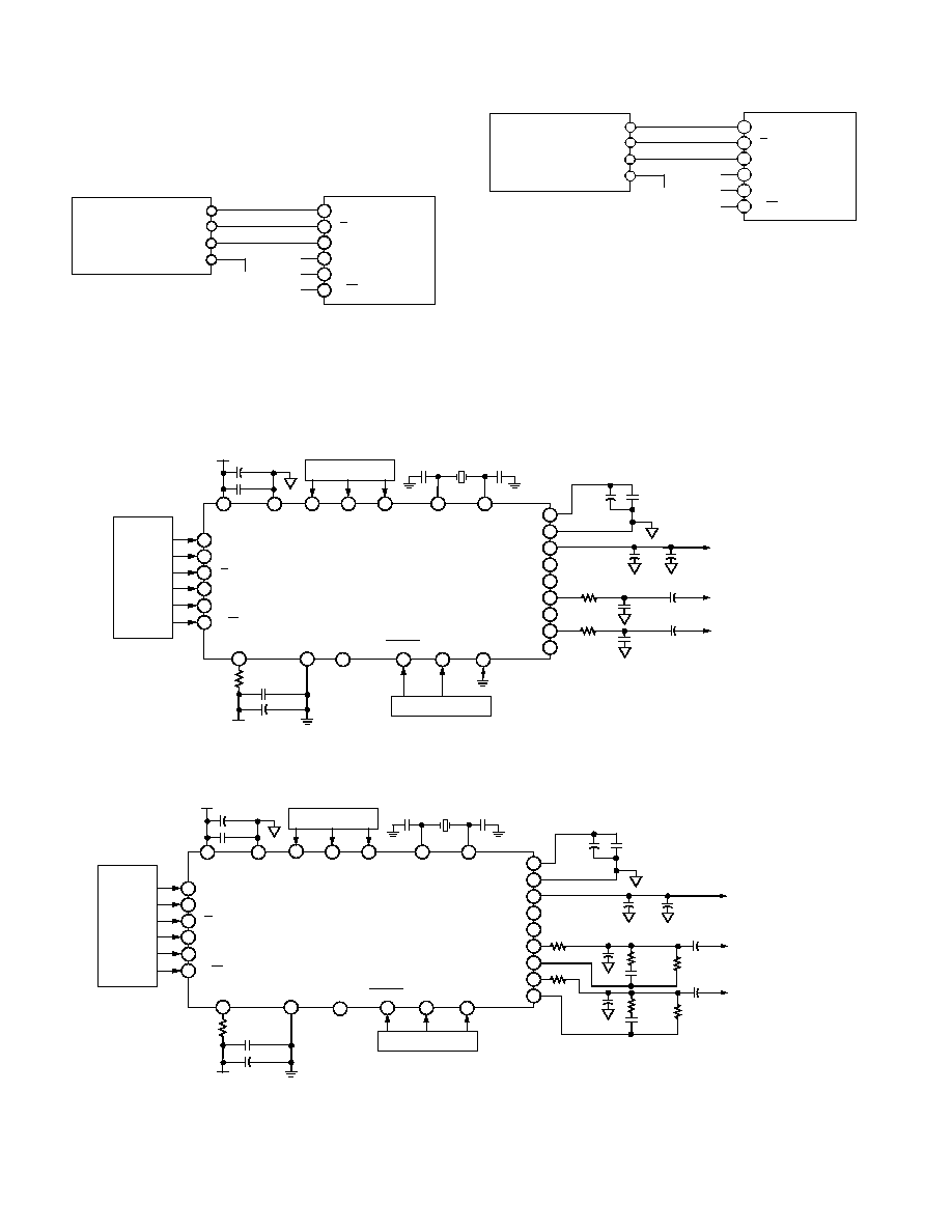
Layout and Decoupling Considerations
The recommended decoupling, bypass circuits for the AD1859
are shown in Figure 17. Figure 17 illustrates a connection dia-
gram for systems which do not require de-emphasis support.
The recommended circuit connection for system including de-
emphasis is shown in Figure 18.
AD1859
10µF
0.1µF
BIAS VOLTAGE
FOR EXTERNAL USE
1k
2.2nF
LEFT LINE
OUTPUT
RIGHT LINE
OUTPUT
10µF
20-64pF
20-64pF
27MHz
XTALI/MCLK
XTALO
CDATA CCLK CLATCH
+5V ANALOG
0.1µF
1µF
AGND
AV
DD
SDATA
BLCK
L
R
CLK
IDPM0
IDPM1
18/
16
10
8
9
12
13
14
DSP OR
AUDIO
DECODER
PD/RST
MUTE
DEEMP
+5V DIGITAL
DGND
DV
DD
FILT
CMOUT
OUTL
EMPL
OUTR
EMPR
AD1859
10µF
2
6
7
15
11
20
16
19
21
22
23
µCONTROLLER
28
24
25
26
27
5
3
NC
NC
FGND
1k
2.2nF
10µF
µCONTROLLER
NC
0.01µF
1µF
17
18
4
1
0.1µF
30
(CHIP RESISTOR
PREFERRED)
Figure 17. Recommended Circuit Connection (Without De-emphasis)
BIAS VOLTAGE
FOR EXTERNAL USE
1k
LEFT LINE
OUTPUT
RIGHT LINE
OUTPUT
1µF
10µF
1k
1µF
470
33nF
NPO
470
OPTIONAL DE-EMPHASIS
CIRCUIT SHOWN
10µF
0.1µF
20-64pF
20-64pF
27MHz
XTALI/MCLK
XTALO
CDATA CCLK CLATCH
+5V ANALOG
0.1µF
1µF
AGND
AV
DD
SDATA
BLCK
L
R
CLK
IDPM0
IDPM1
18/
16
10
8
9
12
13
14
DSP OR
AUDIO
DECODER
PD/RST
MUTE
DEEMP
+5V DIGITAL
DGND
DV
DD
FILT
CMOUT
OUTL
EMPL
OUTR
EMPR
AD1859
2
6
7
15
11
20
16
19
21
22
23
24
27
5
NC
NC
FGND
µCONTROLLER
NC
0.01µF
1µF
17
18
4
1
26
3
25
28
0.1µF
10M
10M
2.2nF
2.2nF
30
(CHIP RESISTOR
PREFERRED)
33nF
NPO
µCONTROLLER
Figure 18. Recommended Circuit Connection (With De-emphasis)

AD1859
REV. A
≠13≠
PCB and Ground Plane Recommendations
The AD1859 ideally should be located above a split ground
plane, with the digital pins over the digital ground plane, and
the analog pins over the analog ground plane. The split should
occur between Pins 6 and 7 and between Pins 22 and 23 as
shown in Figure 19. The ground planes should be tied together
at one spot underneath the center of the package with an ap-
proximately 3 mm trace. This ground plane strategy minimizes
RF transmission and reception as well as maximizes the AD1859's
analog audio performance.
13
1
2
5
6
7
3
4
8
9
10
11
12
14
18
28
27
24
23
22
26
25
21
20
19
17
16
15
CMOUT
DEEMP
NC
EMPL
OUTL
AGND
MUTE
18/
16
IDPM0
IDPM1
SDATA
L
R
CLK
BCLK
PD/RST
ANALOG
GROUND PLANE
DIGITAL
GROUND PLANE
FILT
FGND
NC
AV
DD
NC
EMPR
OUTR
CLATCH
CDATA
CCLK
DGND
DV
DD
XTALI/MCLK
XTALO
Figure 19. Recommended Ground Plane
TIMING DIAGRAMS
The serial data port timing is shown in Figures 20 and 21. The
minimum bit clock HI pulse width is t
DBH
, and the minimum bit
clock LO pulse width is t
DBL
. The minimum bit clock period is
t
DBP
. The left/right clock minimum setup time is t
DLS
, and the
left/right clock minimum hold time is t
DLH
. The serial data mini-
mum setup time is t
DDS
, and the minimum serial data hold time
is t
DDH
.
BCLK
SDATA
LEFT-
JUSTIFIED
MODE
SDATA
RIGHT-
JUSTIFIED
MODE
SDATA
I
2
S-
JUSTIFIED
MODE
MSB
MSB
LSB
t
DBH
t
DBP
t
DBL
t
DLS
t
DDS
t
DDH
t
DDS
t
DDH
t
DDS
t
DDH
t
DDS
t
DDH
MSB
MSB-1
L
R
CLK
Figure 20. Serial Data Port Timing
t
DBH
t
DBL
t
DLS
t
DDH
t
DDS
BCLK
SDATA
LEFT-JUSTIFIED
DSP SERIAL
PORT STYLE
MODE
MSB
MSB-1
t
DBP
t
DLH
L
R
CLK
Figure 21. Serial Data Input Port Timing DSP Serial
Port Style
The serial control port timing is shown in Figure 22. The mini-
mum control clock HI pulse width is t
CCH
, and the minimum
control clock LO pulse width is t
CCL
. The minimum control
clock period is t
CCP
. The control data minimum setup time is
t
CSU
, and the minimum control data hold time is t
CHD
. The
minimum control latch delay is t
CLD
, the minimum control latch
LO pulse width is t
CLL
, and the minimum control latch HI pulse
width is t
CLH
.
CCLK
t
CCL
t
CCP
t
CCH
CDATA
t
CSU
t
CHD
CLATCH
t
CLD
t
CLH
t
CLL
LSB
Figure 22. Serial Control Port Timing
The master clock (or crystal input) and power down/reset tim-
ing is shown in Figure 23. The minimum MCLK period is t
MCP
,
which determines the maximum MCLK frequency at F
MC
. The
minimum MCLK HI and LO pulse widths are t
MCH
and t
MCL
,
respectively. The minimum reset LO pulse width is t
PDRP
(four
XTALI/MCLK periods) to accomplish a successful AD1859 re-
set operation.
PD/RST
XTALI/MCLK
t
PDRP
t
MCH
t
MCP
t
MCL
Figure 23. MCLK and Power Down/Reset Timing

REV. A
≠14≠
AD1859
TYPICAL PERFORMANCE
Figures 24 through 27 illustrate the typical analog performance
of the AD1859 as measured by an Audio Precision System One.
Signal-to-Noise (dynamic range) and THD+N performance is
shown under a range of conditions. Note that there is a small
variance between the AD1859 analog performance specifica-
tions and some of the performance plots. This is because the
Audio Precision System One measures THD and noise over a
20 Hz to 24 kHz bandwidth, while the analog performance is
specified over a 20 Hz to 20 kHz bandwidth (i.e., the AD1859
performs slightly better than the plots indicate). Figure 28
shows the power supply rejection performance of the AD1859.
The channel separation performance of the AD1859 is shown in
Figure 29. The AD1859's low level linearity is shown in Figure
30. The digital filter transfer function is shown in Figure 31.
0
20k
2k
4k
6k
8k
10k
12k
14k
16k
18k
0
≠10
≠90
≠50
≠60
≠70
≠80
≠30
≠40
≠20
≠100
≠110
≠120
≠130
≠140
F
S
= 44.1kHz
FFT @ ≠0.5dBFS
dBFS
FREQUENCY ≠ Hz
Figure 24. 1 kHz Tone at ≠0.5 dBFS (16K-Point FFT)
0
20k
2k
4k
6k
8k
10k
12k
14k
16k
18k
0
≠10
≠90
≠50
≠60
≠70
≠80
≠30
≠40
≠20
≠100
≠110
≠120
≠130
≠140
F
S
= 44.1kHz
FFT @ ≠10dBFS
dBFS
FREQUENCY ≠ Hz
Figure 25. 1 kHz Tone at ≠10 dBFS (16K-Point FFT)
0
20k
2k
4k
6k
8k
10k
12k
14k
16k
18k
0
≠10
≠90
≠50
≠60
≠70
≠80
≠30
≠40
≠20
≠100
≠110
F
S
= 44.1kHz
THD+N vs FREQ @ ≠0.5dBFS
dBFS
FREQUENCY ≠ Hz
Figure 26. THD+N vs. Frequency at ≠0.5 dBFS
≠100
0
≠90
≠80
≠70
≠60
≠50
≠40
≠30
≠20
≠10
0
≠10
≠90
≠50
≠60
≠70
≠80
≠30
≠40
≠20
≠100
≠110
dBFS
AMPLITUDE ≠ dBFS
FS = 44.1kHz
THD+N vs dBFS @ 1kHz
Figure 27. THD+N vs. Amplitude at 1 kHz
0
20k
2k
4k
6k
8k
10k
dBFS
12k
14k
16k
18k
≠40
≠45
≠65
≠70
≠75
≠80
≠55
≠60
≠50
LEFT CHANNEL
RIGHT CHANNEL
FREQUENCY ≠ Hz
Figure 28. Power Supply Rejection to 300 mV p-p on AV
DD
0
20k
2k
4k
6k
8k
10k
12k
14k
16k
18k
0
≠10
≠90
≠50
≠60
≠70
≠80
≠30
≠40
≠20
≠100
≠110
≠120
dBFS
FREQUENCY ≠ Hz
F
S
= 44.1kHz
Figure 29. Channel Separation vs. Frequency at ≠0.5 dBFS
AD1859
REV. A
≠15≠
0
20k
2k
4k
6k
8k
10k
12k
14k
16k
18k
0
≠10
≠90
≠50
≠60
≠70
≠80
≠30
≠40
≠20
≠100
≠110
≠120
≠130
≠140
22k
10
0%
100
90
FREQUENCY ≠ Hz
dBFS
Figure 30. 1 kHz Tone at ≠90 dBFS (16K-Point FFT) Includ-
ing Time Domain Plot Bandlimited to 22 kHz
0.0
3.5
0.5
1.0
1.5
2.0
2.5
3.0
0
≠10
≠90
≠50
≠60
≠70
≠80
≠30
≠40
≠20
≠100
≠110
≠120
≠130
≠140
≠150
≠160
dBFS
F
S
Figure 31. Digital Filter Signal Transfer Function to
3.5
◊
F
S
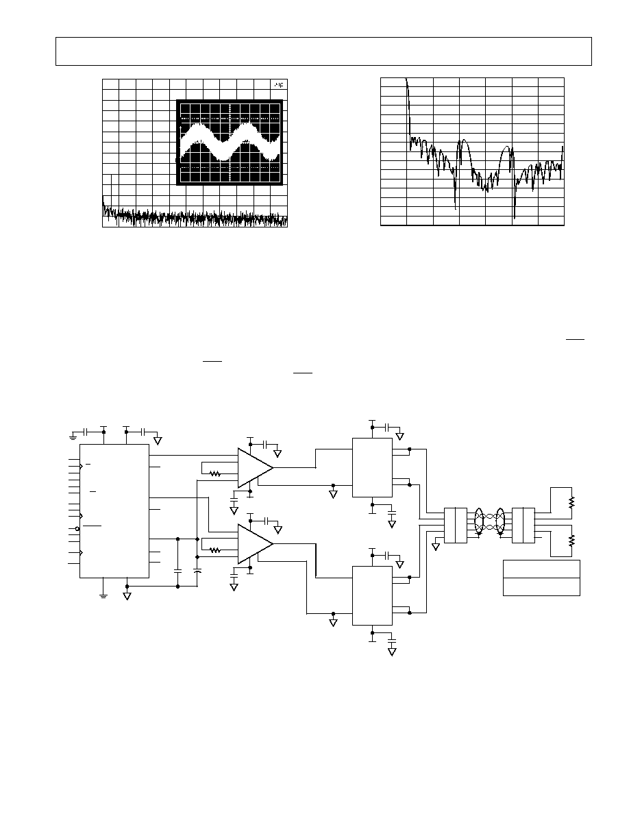
Application Circuits
Figure 32 illustrates a 600 ohm line driver using the Analog
Devices SSM2017 and SSM2142 components. Figure 33
illustrates a "Numerically Controlled Oscillator" (NCO) that
can be implemented in programmable logic or a system ASIC to
provide the synchronous bit and left/right clocks from 27 MHz
for MPEG audio decoders. Note that the bit clock and left/right
clock outputs are highly jittered, but this jitter should be
perfectly acceptable. MPEG audio decoders are insensitive to
this clock jitter (using these signals to clock audio data from their
output serial port, and perhaps to decrement their audio/video
synchronization timer), while the AD1859 will reject the left/right
clock jitter by virtue of its on-chip digital phase locked loop.
Contact Analog Devices Computer Products Division Customer
Support at (617) 461-3881 or cpd_support@analog.com for more
information on this NCO circuit.
BCLK
L
R
CLK
SDATA
IDPM1
IDPM0
18/
16
CLATCH
CDATA
CCLK
PD/RST
DEEMP
MUTE
XTALI/MCLK
XTALO
FGND
FILT
CMOUT
EMPR
OUTR
EMPL
OUTL
DV
DD
AV
DD
DGND
AGND
14
13
12
10
9
8
21
20
19
11
2
7
16
15
4
3
25
26
1
28
27
3
1
8
2
3
1
8
2
7
7
6
6
5
4
5
4
U2
SSM2017P
U3
SSM2017P
+15V
≠15V
+15V
≠15V
1Vrms
1Vrms
OUT
OUT
REF
REF
V+
V≠
V+
V≠
V
REF
2.25V
+5V
CC
+5V
DD
17
23
18
6
R2, 2k49
R1, 2k49
C8
100n
C1
100n
C9
100n
+
≠
C10
C7
100n
C6
100n
C12
100n
C11
100n
AD1859-JR
GND
V
IN
+V
≠V
+OUT
+SENSE
≠SENSE
≠OUT
U4
SSM2142P
6
+15V
C5
100n
≠15V
C4
100n
4
3
5
8
7
2
1
GND
V
IN
+V
≠V
+OUT
+SENSE
U5
SSM2142P
6
+15V
C3
100n
≠15V
C2
100n
4
3
5
8
7
2
1
5Vrms
5Vrms
1
2
3
4
5
1
2
3
4
5
J1
P1
1
2
3
4
5
1
2
3
4
5
P2
J2
R3
600
R4
600
MAX OUTPUT EACH
CHANNEL
10Vrms (166.7mV V = +22dBm)
INTO 600
≠SENSE
≠OUT
+IN
RG
1
RG
2
≠IN
4µ7
+IN
RG
1
RG
2
≠IN
Figure 32. 600 Ohm Balanced Line Driver
REV. A
≠16≠
AD1859
C2123≠18≠4/96
2 TO 1
SELECTOR
1
0
13
13-BIT
ADDER
+
_
13
13
13
RI BUS
K BUS
R BUS
27 MHz
T
Q
BCLK
13-BIT
LATCH
27MHz
13-BIT
ADDER
+
13
13
M [12..0]
+
L BUS
N [12..0]
13
SELECT K BUS WHEN K < N (MSB = 0)
SELECT R BUS WHEN K > N (MSB = 1)
MSB
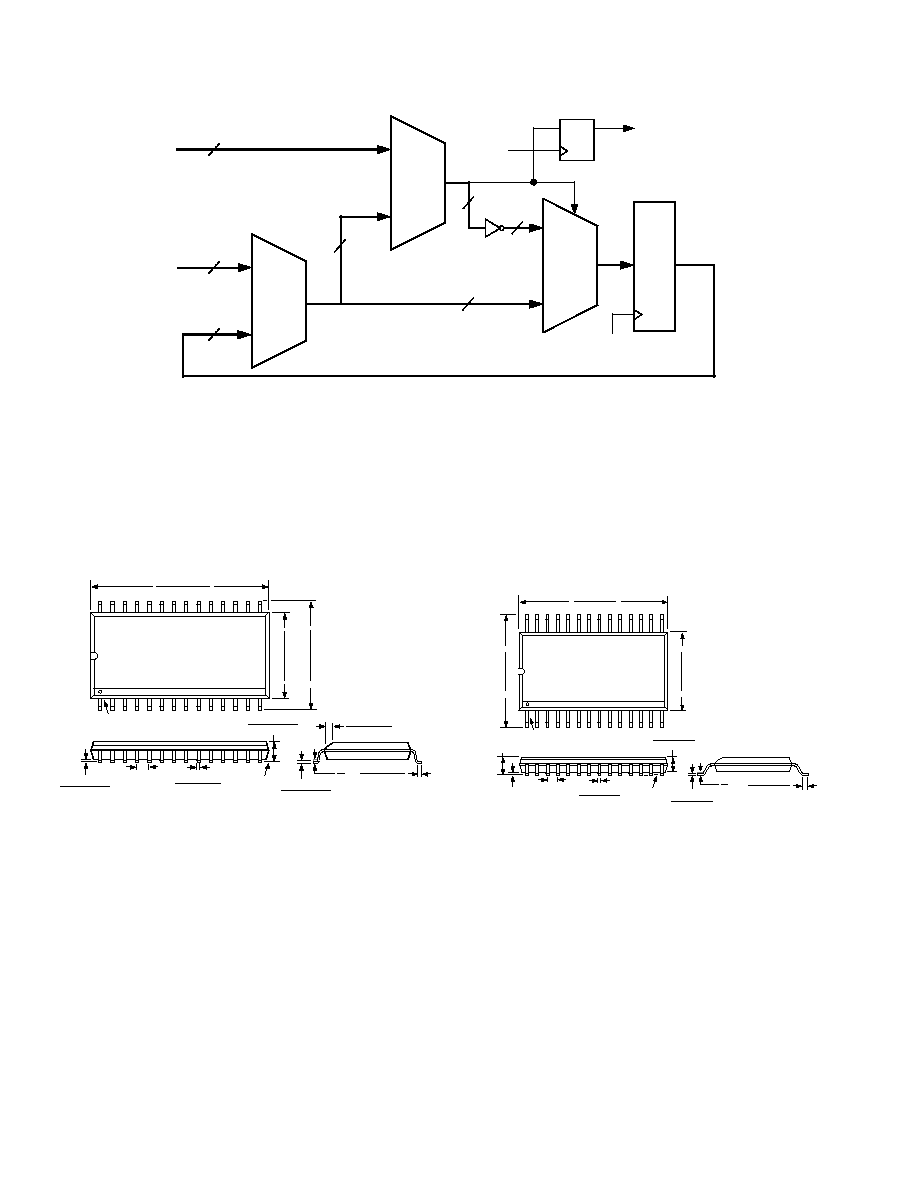
Figure 33. Numerically Controlled Oscillator Circuit
PRINTED IN U.S.A.
28-Lead Wide-Body SO
(R-28)
28
15
14
1
0.7125 (18.10)
0.6969 (17.70)
0.419 (10.65)
0.394 (10.00)
0.2992 (7.60)
0.2914 (7.40)
PIN 1
SEATING
PLANE
0.0118 (0.30)
0.0040 (0.10)
0.020 (0.49)
0.013 (0.35)
0.1043 (2.65)
0.0926 (2.35)
0.0500
(1.27)
BSC
0.0125 (0.32)
0.0091 (0.23)
0.050 (1.27)
0.016 (0.40)
8
∞
0
∞
0.029 (0.74)
0.010 (0.25)
x 45
∞
28-Lead Shrink Small Outline Package (SSOP)
(RS-28)
28
15
14
1
0.41 (10.50)
0.39 (9.90)
0.32 (8.20)
0.29 (7.40)
0.22 (5.60)
0.20 (5.00)
PIN 1
SEATING
PLANE
0.073 (1.85)
0.065 (1.65)
0.026
(0.65)
BSC
0.015 (0.38)
0.009 (0.22)
0.002 (0.05)
MIN
0.079 (2.0)
MAX
0.01 (0.25)
0.004 (0.09)
0.037 (0.95)
0.022 (0.55)
8
∞
0
∞
OUTLINE DIMENSIONS
Dimensions shown in inches and (mm).