 | –≠–ª–µ–∫—Ç—Ä–æ–Ω–Ω—ã–π –∫–æ–º–ø–æ–Ω–µ–Ω—Ç: AD1862 | –°–∫–∞—á–∞—Ç—å:  PDF PDF  ZIP ZIP |

FUNCTIONAL BLOCK DIAGRAM
VOLTAGE
REFERENCE
INPUT
&
DIGITAL
OFFSET
20-BIT
DAC
AD1862
1
2
3
4
5
6
7
8
16
15
14
13
12
11
10
9
≠V
S
≠V
S
TRIM
+V
L
CLK
DATA
LE
≠V
L
+V
S
NR
2
ADJ
NR
1
AGND
I
OUT
R
F
DGND
REV. A
Information furnished by Analog Devices is believed to be accurate and
reliable. However, no responsibility is assumed by Analog Devices for its
use, nor for any infringements of patents or other rights of third parties
which may result from its use. No license is granted by implication or
otherwise under any patent or patent rights of Analog Devices.
a
Ultralow Noise
20-Bit Audio DAC
AD1862*
One Technology Way, P.O. Box 9106, Norwood, MA 02062-9106, U.S.A.
Tel: 617/329-4700
Fax: 617/326-8703
FEATURES
120 dB Signal-to-Noise Ratio
102 dB D-Range Performance
1 dB Gain Linearity
1 mA Output Current
16-Pin DIP Package
0.0012% THD + N
APPLICATIONS
High Performance Compact Disc Players
Digital Audio Amplifiers
Synthesizer Keyboards
Digital Mixing Consoles
High Resolution Signal Processing
PRODUCT DESCRIPTION
The AD1862 is a monolithic 20-bit digital audio DAC. Each
device provides a 20-bit DAC, 20-bit serial-to-parallel input
register and voltage reference. The digital portion of the
AD1862 is fabricated with CMOS logic elements that are pro-
vided by Analog Devices' BiMOS II process. The analog por-
tion of the AD1862 is fabricated with bipolar and MOS devices
as well as thin-film resistors.
New design, layout and packaging techniques all combine to
produce extremely high performance audio playback. The de-
sign of the AD1862 incorporates a digital offset circuit which
improves low-level distortion performance. Low stress packag-
ing techniques are used to minimize stress-induced parametric
shifts. Stress-sensitive circuit elements are located in die areas
which are least affected by packaging stress. Laser-trimming of
initial linearity error affords extremely low total harmonic
distortion. Output glitch is also small, contributing to the over-
all high level of performance.
The noise performance of the AD1862 is excellent. When used
with the recommended two external noise-reduction capacitors,
it achieves 120 dB signal-to-noise ratio.
The serial input port consists of the clock, data and latch enable
pins. A serial 20-bit, 2s complement data word is clocked into
the DAC, MSB first, by the external data clock. A latch-enable
signal transfers the input word from the internal serial input
register to the DAC input register. The data clock can function
at 17 MHz, allowing 16
◊
F
S
operation. The serial input port is
compatible with second-generation digital filter chips for con-
sumer audio products such as the NPC SM5813 and SM5818.
The AD1862 operates with
±
5 V to
±
12 V supplies for the dig-
ital power supplies and
±
12 V supplies for the analog supplies.
The digital and analog supplies can be separated for reduced
digital crosstalk. Separate analog and digital common pins are
also provided. The AD1862 typically dissipates less than
300 mW.
The AD1862 is packaged in a 16-pin plastic DIP. The operating
range is guaranteed to be ≠25
∞
C to +70
∞
C.
PRODUCT HIGHLIGHTS
1. 120 dB signal-to-noise ratio. (typical)
2. 102 dB D-Range performance. (minimum)
3.
±
1 dB gain linearity @ ≠90 dB amplitude.
4. 20-bit resolution provides 120 dB of dynamic range.
5. 16
◊
F
S
operation.
6. 0.0016% THD+N @ 0 dB signal amplitude. (typical)
7. Space saving 16-pin DIP package.
8.
±
1 mA output current.
*Protected by U.S. Patent Numbers: 4,349,811; 4,857,862; 4,855,618;
3,961,326; 4,141,004; 4,902,959.

AD1862≠SPECIFICATIONS
Min
Typ
Max
Units
RESOLUTION
20
Bits
DIGITAL INPUTS V
IH
2.0
4.0
V
V
IL
0.4
0.8
V
I
IH
@ V
IH
= 4.0 V
1.0
µ
A
I
IL
@ V
IL
= 0.4 V
≠10
µ
A
Maximum Clock Input Frequency
17
MHz
ACCURACY
Gain Error
±
2
%
Midscale Output Error
±
2
±
5
µ
A
TOTAL HARMONIC DISTORTION + NOISE (EIAJ)
1
0 dB, 990.5 Hz
AD1862N-J
≠98 (0.0012)
≠96 (0.0016)
dB (%)
AD1862N
≠94 (0.0019)
≠92 (0.0025)
dB (%)
≠20 dB, 990.5 Hz AD1862N, N-J
≠84 (0.0063)
≠80 (0.01)
dB (%)
≠60 dB, 990.5 Hz AD1862N, N-J
≠45 (0.56)
≠42 (0.8)
dB (%)
D-Range, ≠60 dB, A-Weight Filter
102
dB
SIGNAL-TO-NOISE RATIO
2
: (EIAJ)
1
A-Weight Filter
AD1862N-J
113
119
dB
AD1862N
110
119
dB
GAIN LINEARITY
@ ≠90 dB
AD1862N-J
±
1
dB
AD1862N
±
1
dB
OUTPUT CURRENT
Bipolar Range
±
1
mA
Tolerance
±
1
2
%
Output Impedance (
±
30%)
2.1
k
Settling Time
350
ns
FEEDBACK RESISTOR
Value
3
k
Tolerance
±
1
2
%
POWER SUPPLY
Voltage
V
L
and ≠V
L
4.75
12.0
13.2
±
V
Voltage
V
S
and ≠V
S
10.8
12.0
13.2
±
V
Current
+I, V
L
and V
S
= 12 V, 17 MHz Clock
11
15
mA
≠I, ≠V
L
and ≠V
S
= ≠12 V, 17 MHz Clock
13
16
mA
POWER DISSIPATION
V
L
and V
S
= 12 V, ≠V
L
and ≠V
S
= ≠12 V, 17 MHz Clock
288
372
mW
TEMPERATURE RANGE
Specification
+25
∞
C
Operation
≠25
+70
∞
C
Storage
≠60
+100
∞
C
NOTES
1
Test Method complies with EIAJ Standard CP-307.
2
The signal-to-noise measurement includes noise contributed by the SE5534A op amp used in the test fixture but does not include the noise contributed by the low
pass filter used in the test fixture.
Specifications in boldface are tested on all production units at final electrical test.
Specifications subject to change without notice.
REV. A
≠2≠
(T
A
at +25 C and 12 V supplies, see Figure 10 for test circuit schematic)
AD1862
≠3≠
REV. A
20
≠80
≠90
1
≠60
≠70
≠50
≠40
≠30
10
≠60dB
≠20dB
0dB
THD +N ≠ dB
FREQUENCY ≠ kHz
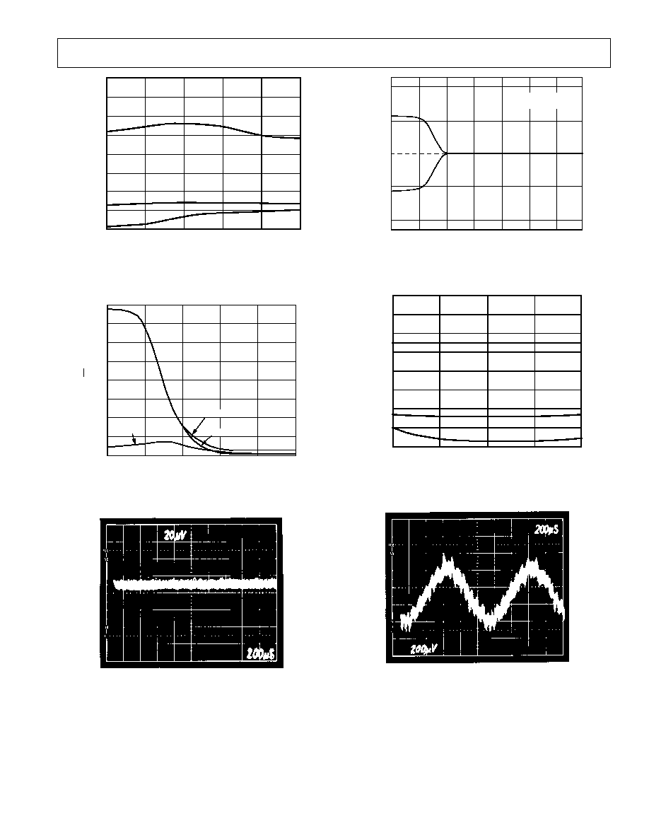
Figure 1. THD+N vs. Frequency
MIDSCALE
FULLSCALE
≠FULLSCALE
1
10
100
1k
10k
100k
Hz
400
350
300
250
200
150
100
50
0
nV/
Hz
Figure 2. Noise Density
Figure 3. Broadband Noise (20 kHz Bandwidth, Midscale)
AD1862N-J
GAIN LINEARITY
0
100
≠
80
≠
60
≠
40
≠
20
≠
DIGITAL INPUT ≠ dB
2
1
1
≠
2
≠
ANALOG OUTPUT ERROR ≠ dB
Figure 4. Gain Linearity
≠30
≠40
≠50
≠60
≠70
≠80
≠90
THD N ≠ dB
+
≠60dB
0dB
≠20dB
≠25
0
25
50
75
TEMPERATURE ≠ ∞C
Figure 5. THD+N vs. Temperature (1 kHz)
Figure 6. Midscale Differential Linearity

AD1862
≠4≠
REV. A
ABSOLUTE MAXIMUM RATINGS*
V
L
to DGND . . . . . . . . . . . . . . . . . . . . . . . . . . . . 0 to +13.2 V
≠V
L
to DGND . . . . . . . . . . . . . . . . . . . . . . . . . . . . . ≠V
S
to 0 V
V
S
to AGND . . . . . . . . . . . . . . . . . . . . . . . . . . . . 0 to +13.2 V
≠V
S
to AGND . . . . . . . . . . . . . . . . . . . . . . . . . . . ≠13.2 to 0 V
AGND to DGND . . . . . . . . . . . . . . . . . . . . . . . ≠0.3 to +0.3 V
Digital Inputs to DGND . . . . . . . . . . . . . . . . . . . . . ≠0.3 to V
L
Soldering . . . . . . . . . . . . . . . . . . . . . . . . . . . . . +300
∞
C, 10 sec
Storage Temperature . . . . . . . . . . . . . . . . . . ≠60
∞
C to +100
∞
C
*Stresses greater than those listed under "Absolute Maximum Ratings" may cause
permanent damage to the device. This is a stress rating only and functional
operation of the device at these or any other conditions above those indicated in the
operational section of this specification is not implied. Exposure to absolute
maximum rating conditions for extended periods may affect device reliability.
WARNING!
ESD SENSITIVE DEVICE
CAUTION
ESD (electrostatic discharge) sensitive device. Electrostatic charges as high as 4000 V readily
accumulate on the human body and test equipment and can discharge without detection.
Although the AD1862 features proprietary ESD protection circuitry, permanent damage may
occur on devices subjected to high energy electrostatic discharges. Therefore, proper ESD
precautions are recommended to avoid performance degradation or loss of functionality.
PIN CONFIGURATION
PIN DESIGNATIONS
Pin
Function
Description
1
1
≠V
S
Bias Capacitor
1
2
≠V
S
Analog Negative Supply
1
3
TRIM
Trim Pot Connection
1
4
+V
L
Positive Logic Supply
1
5
CLK
External Clock Input
1
6
LE
Latch Enable Input
1
7
D
Data Input
1
8
≠V
L
Negative Logic Supply
1
9
DGND
Digital Ground
10
R
F
Feedback Resistor
11
I
OUT
Output Current
12
AGND
Analog Ground
13
NR
1
Reference Capacitor
14
ADJ
Midscale Adjust
15
NR
2
Bias Capacitor
16
+V
S
Positive Analog Supply
ORDERING GUIDE
Operating
Temperature
Package
Model
Range
THD+N @ FS
SNR
Option*
AD1862N
≠25
∞
C to +70
∞
C
≠92 dB, 0.0025%
110 dB
N-16
AD1862N-J
≠25
∞
C to +70
∞
C
≠96 dB, 0.0016%
113 dB
N-16
*N = Plastic DIP.
AD1862
TOP VIEW
(Not to Scale)
1
2
3
4
5
6
7
8
9
10
11
12
13
14
15
16
≠V
S
TRIM
+V
L
CLK
LE
DATA
NR
2
ADJ
NR
1
AGND
I
OUT
R
F
DGND
≠V
S
≠V
L
+V
S
AD1862
≠5≠
REV. A
TOTAL HARMONIC DISTORTION + NOISE
Total Harmonic Distortion plus Noise (THD+N) is defined as
the ratio of the square root of the sum of the squares of the val-
ues of the harmonics and noise to the value of the fundamental
input frequency. It is usually expressed in percent (%) or deci-
bels (dB).
D-RANGE DISTORTION
D-Range Distortion is the ratio of the signal amplitude to the
distortion plus noise at ≠60 dB. In this case, an A-Weight filter
is used. The value specified for D-Range performance is the ra-
tio measured plus 60 dB.
SETTLING TIME
Settling Time is the time required for the output to reach and
remain within
±
1/2 LSB about its final value, measured from
the digital input transition. It is a primary measure of dynamic
performance and is usually expressed in nanoseconds (ns).
SIGNAL-TO-NOISE RATIO
The Signal-to-Noise Ratio is defined as the ratio of the ampli-
tude of the output with full-scale present to the amplitude of the
output when no signal is present. It is expressed in decibels (dB)
and measured using an A-Weight filter.
GAIN LINEARITY
Gain Linearity is a measure of the deviation of the actual output
amplitude from the ideal output amplitude. It is determined by
measuring the amplitude of the output signal as the amplitude
of that output signal is digitally reduced to a low level. A perfect
D/A converter exhibits no difference between the ideal and ac-
tual amplitudes. Gain linearity is expressed in decibels (dB).
MIDSCALE ERROR
Midscale Error, or bipolar zero error, is the deviation of the ac-
tual analog output from the ideal output when the 2s comple-
ment input code representing midscale is loaded in the input
register. The AD1862 is a current output D/A converter. There-
fore, this error is expressed in
µ
A.
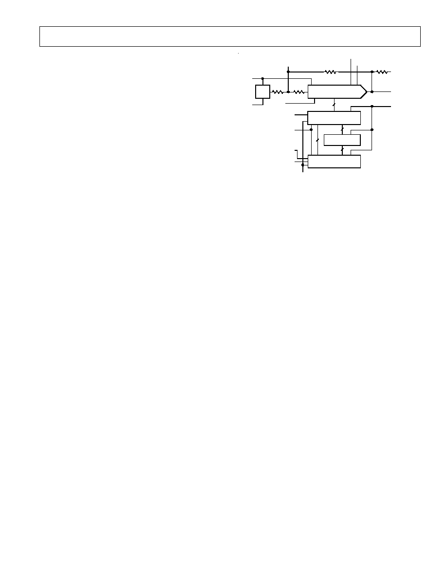
DECODER AND
DIGITAL OFFSET
20-BIT DAC
LATCH
SERIAL INPUT
REGISTER
TRIM
ADJ
FEEDBACK
REGISTER
CURRENT
OUTPUT
V
L
+
NR1
V
S
AGND
V
REF
NR2
≠ V
L
LATCH
ENABLE
CLOCK
DATA
DGND
AD1862 Block Diagram
FUNCTIONAL DESCRIPTION
The AD1862 is a high performance, monolithic 20-bit audio
DAC. Each device includes a voltage reference, a 20-bit DAC,
20-bit input latch and a 20-bit serial-to-parallel input register. A
special digital offset circuit, combined with segmentation cir-
cuitry, produces excellent THD+N and D-range performance.
Extensive noise-reduction features are utilized to make the noise
performance of the AD1862 as high as possible. For example,
the voltage reference circuit is a low-noise, 9 volt bandgap cell.
This cell supplies the reference voltage to the bipolar offset cir-
cuit and the DAC. An external noise-reduction capacitor is con-
nected to NR1 to form a low-pass filter network.
Additional noise-reduction techniques are used in the control
amplifier of the DAC. By connecting an external noise-reduction
capacitor to NR2 output noise contributions from the control
portion of the DAC are similarly reduced. The noise-reduction
efforts result in a signal-to-noise ratio of 120 dB.
The design of the AD1862 uses a combination of segmented de-
coder, R-2R topology and digital offset to produce low distor-
tion at all signal amplitudes. The digital offset technique shifts
the midscale output voltage (0 V) away from the MSB transition
of the device. Therefore, small amplitude signals are not af-
fected by an MSB change. An extra DAC cell is included to
avoid clipping the output at full scale.
The DAC supplies a
±
1 mA output current to an external
I-to-V converter. An on-board 3 k
feedback resistor is also
supplied. Both the output current and feedback resistor are
laser-trimmed to
±
2% tolerance, simplifying the selection of
external filter and/or deemphasis network components. The in-
put register and serial-to-parallel converter are fabricated with
CMOS logic gates. These gates allow the achievement of fast
switching speeds and low power consumption. Internal TTL-
to-CMOS converters are used to insure TTL and 5 V CMOS
compatibility.
AD1862
≠6≠
REV. A
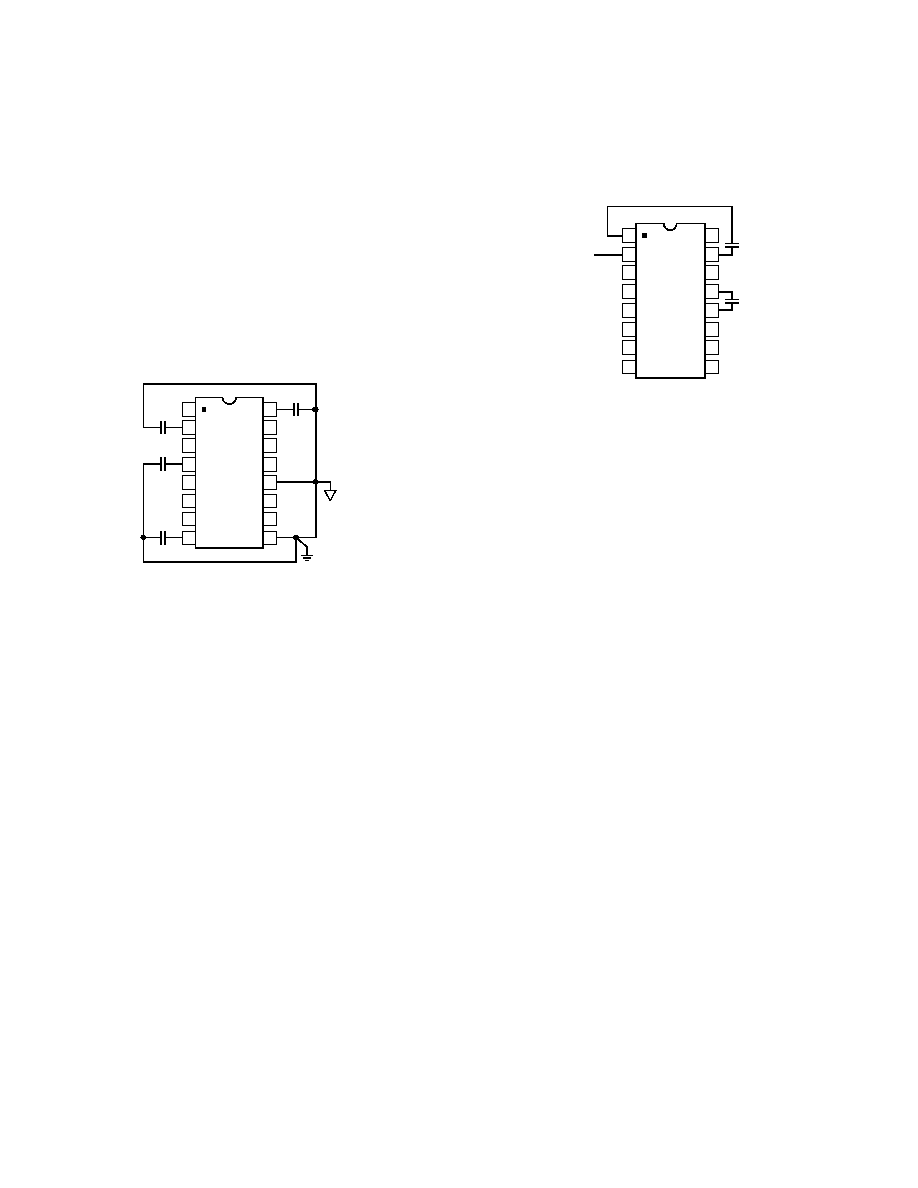
Analog Circuit Considerations
GROUNDING RECOMMENDATIONS
The AD1862 has two ground pins, designated analog ground
(AGND) and digital ground (DGND). The analog ground pin
is the "high-quality" ground reference for the device. The ana-
log ground pin should be connected to the analog common
point in the system. The reference bypass capacitor, the nonin-
verting terminal of the current-to-voltage conversion op amp,
and any output loads should be connected to this point. The
digital ground pin returns ground current from the digital logic
portions of the AD1862 circuitry. This pin should be connected
to the digital common point in the system.
As illustrated in Figure 7, AGND and DGND should be con-
nected together at one point in the system.
AD1862
TOP VIEW
(Not to Scale)
1
2
3
4
5
6
7
8
9
10
11
12
13
14
15
16
DGND
AGND
Figure 7. Grounding and Bypassing Recommendations
POWER SUPPLIES AND DECOUPLING
The AD1862 has four power supply input pins.
±
V
S
provide the
supply voltages which operate the linear portions of the DAC in-
cluding the voltage reference and control amplifier. The
±
V
S
supplies are designed to operate with
±
12 volts.
The
±
V
L
supplies operate the digital portions of the chip includ-
ing the input shift register, the input latching circuitry and the
TTL-to-CMOS level shifters. The
±
V
L
supplies are designed to
be operated from
±
5 V to
±
12 V supplies subject only to the
limitation that ≠V
L
may not be more negative than ≠V
S
.
Decoupling capacitors should be used on all power supply input
pins. Good engineering practice suggests that these capacitors
be placed as close as possible to the package pins and the com-
mon points. The logic supplies,
±
V
L
, should be decoupled to
DGND and the analog supplies,
±
V
S
, should be decoupled to
AGND.
EXTERNAL NOISE REDUCTION COMPONENTS
Two external capacitors are required to achieve low-noise opera-
tion. Their correct connection is illustrated in Figure 8. Capacitor
C1 is connected between the pin labeled NR1 and analog com-
mon. C1 forms a low-pass filter element which reduces noise con-
tributed by the voltage reference circuitry. The proper choice for
this capacitor is a tantalum type with value of 10
µ
F or more. This
capacitor should be connected to the package pins as closely as
possible. This will minimize the effects of parasitic inductance of
the leads and connections circuit connections.
≠12V
ANALOG
SUPPLY
C2
C1
AD1862
TOP VIEW
(Not to
Scale)
1
2
3
4
5
6
7
8
9
10
11
12
13
14
15
16
+
+
NOTE:
PIN 1 IS "HIGH QUALITY" RETURN
FOR BIAS CAP.
Figure 8. Noise Reduction Capacitors
Capacitor C2 is connected between the pin labeled NR2 and the
negative analog supply, ≠V
S
. This capacitor reduces the portion
of output noise contributed by the control amplifier circuitry.
C2 should be chosen to be a tantalum capacitor with a value of
about 1
µ
F. Again, the connections between the AD1862 and
C2 should be made as short as possible.
The recommended values for C1 and C2 are 10
µ
F and 1
µ
F,
respectively. The ratio between C1 and C2 should be approxi-
mately 10. Additional noise reduction can be gained by choos-
ing slightly higher values for C1 and C2 such as 22
µ
F and
2.2
µ
F. Figure 2 illustrates the noise performance of the
AD1862 with 10
µ
F and 1
µ
F.
EXTERNAL AMPLIFIER CONNECTIONS
The AD1862 is a current-output D/A converter. Therefore, an
external amplifier, in combination with the on-board feedback
resistor, is required to derive an output voltage. Figure 9 illus-
trates the proper connections for an external operational ampli-
fier. The output of the AD1862 is intended to drive the
summing junction of an external current-to-voltage conversion
op amp. Therefore, the voltage on the output current pin of the
AD1862 should be approximately the same as that on the
AGND pin of the device.
The on-board 3 k
feedback resistor and the
±
1 mA output
current typically have
±
1% tolerance or less. This makes the
choice of external components very simple and eliminates addi-
tional trimming. For example, if a user wishes to derive an out-
put voltage higher than the
±
3 V swing offered by the output
current and feedback resistor combination, all that is required is
to combine a standard value resistor with the feedback resistor
to achieve the appropriate output voltage swing. This technique
can be extended to include the choice of elements in the
deemphasis network, etc.
TOTAL HARMONIC DISTORTION + NOISE
The THD figure of an audio DAC represents the amount of un-
desirable signal produced during reconstruction and playback of
an audio waveform. The THD specification, therefore, provides
a direct method to classify and choose an audio DAC for a de-
sired level of performance.
By combining noise measurement with the THD measurement,
a THD+N specification is realized. This specification indicates
all of the undesirable signal produced by the DAC, including
harmonic products of the test tone as well as noise.
Analog Devices tests all AD1862s on the basis of THD+N per-
formance. In this test procedure, a digital data stream represent-
ing a 0 dB, ≠20 dB or ≠60 dB sine wave is sent to the device
under test. The frequency of the waveform is 990.5 Hz. Input
data is sent to the AD1862 at an 8
◊
F
S
rate (352.8 kHz). The
AD1862 under test produces an output current which is con-
verted to an output voltage by an external amplifier. Figure 10
illustrates the recommended test circuit. Deglitchers and trims
are not used during this test procedure. The automatic test
equipment digitizes 4096 samples of the output test waveform,
incorporating 23 complete cycles of the sine wave. A 4096 point
FFT is performed on the test data.
V
OUT
AD1862
TOP VIEW
(Not to Scale)
1
2
3
4
5
6
7
8
9
10
11
12
13
14
15
16
Figure 9. External Amplifier Connections
Based upon the harmonics of the fundamental 990.5 Hz test
tone, and the noise components in the audio band, the total har-
monic distortion + noise of the device is calculated. The
AD1862 is available in two performance grades. The AD1862N
produces a maximum of 0.0025% THD+N at 0 dB signal lev-
els. The higher performance AD1862N-J produces a maximum
of 0.0016% THD+N at 0 dB signal levels.
SIGNAL-TO-NOISE RATIO
The Signal-to-Noise Ratio (SNR) of the AD1862 is tested in the
following manner. The amplitude of a 0 dB signal is measured.
The device under test is then set to midscale output voltage (0
volts). The amplitude of all noise present to 30 kHz is mea-
sured. The SNR is the ratio of these two measurements. The
SNR figure for the AD1862 includes the output noise contrib-
uted by the NE5534 op amp used in the test fixture but does
not include the noise contributed by the low-pass filter used in
the test fixture.
The AD1862N has a minimum SNR of 110 dB. The higher
performance AD1862N-J has a minimum SNR of 113 dB.
Testing the AD1862
REV. A
≠7≠
AD1862
TOP VIEW
(Not to Scale)
1
2
3
4
5
6
7
8
9
10
11
12
13
14
15
16
0.1
µ
F
0.1
µ
F
0.1
µ
F
0.1
µ
F
10
µ
F
1
µ
F
3-POLE
LOW PASS
FILTER
12V
≠
12V
12V
≠
17MHz
352.8kHz
DIGITAL
COMMON
SE5534A
OUTPUT
VOLTAGE
ANALOG
COMMON
12V
360pF
+
+
Figure 10. Recommended Test Circuit
AD1862
≠8≠
REV. A
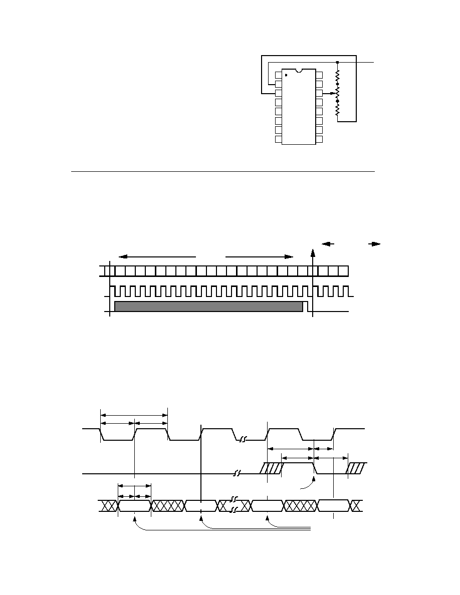
OPTIONAL TRIM ADJUSTMENT
The AD1862 includes an external midscale adjust feature.
Should an application require improved distortion performance
under small and very small signal amplitudes (≠60 dB and
lower), an adjustment is possible. Two resistors and one poten-
tiometer form the adjustment network. Figure 11 illustrates the
correct configuration of the external components. Analog
Devices recommends that this adjustment be performed with
≠60 dB signal amplitudes or lower. Minor performance im-
provement is achieved with larger signal amplitudes such as
≠20 dB. Almost no improvement is possible when this adjust-
ment is performed with 0 dB signal amplitudes.
470k
470k
100k
AD1862
TOP VIEW
(Not to Scale)
1
2
3
4
5
6
7
8
9
10
11
12
13
14
15
16
≠ 12V
Figure 11. External Midscale Adjust
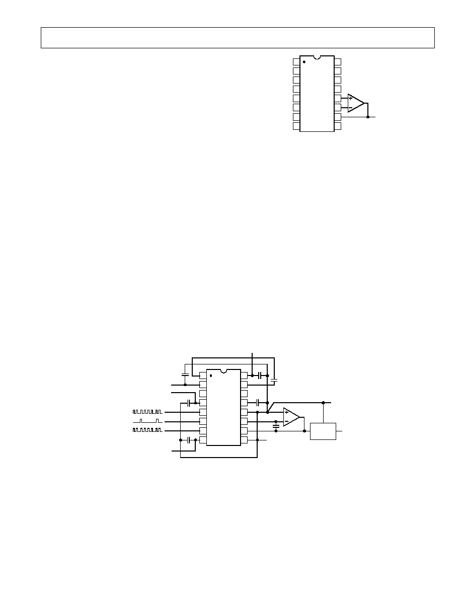
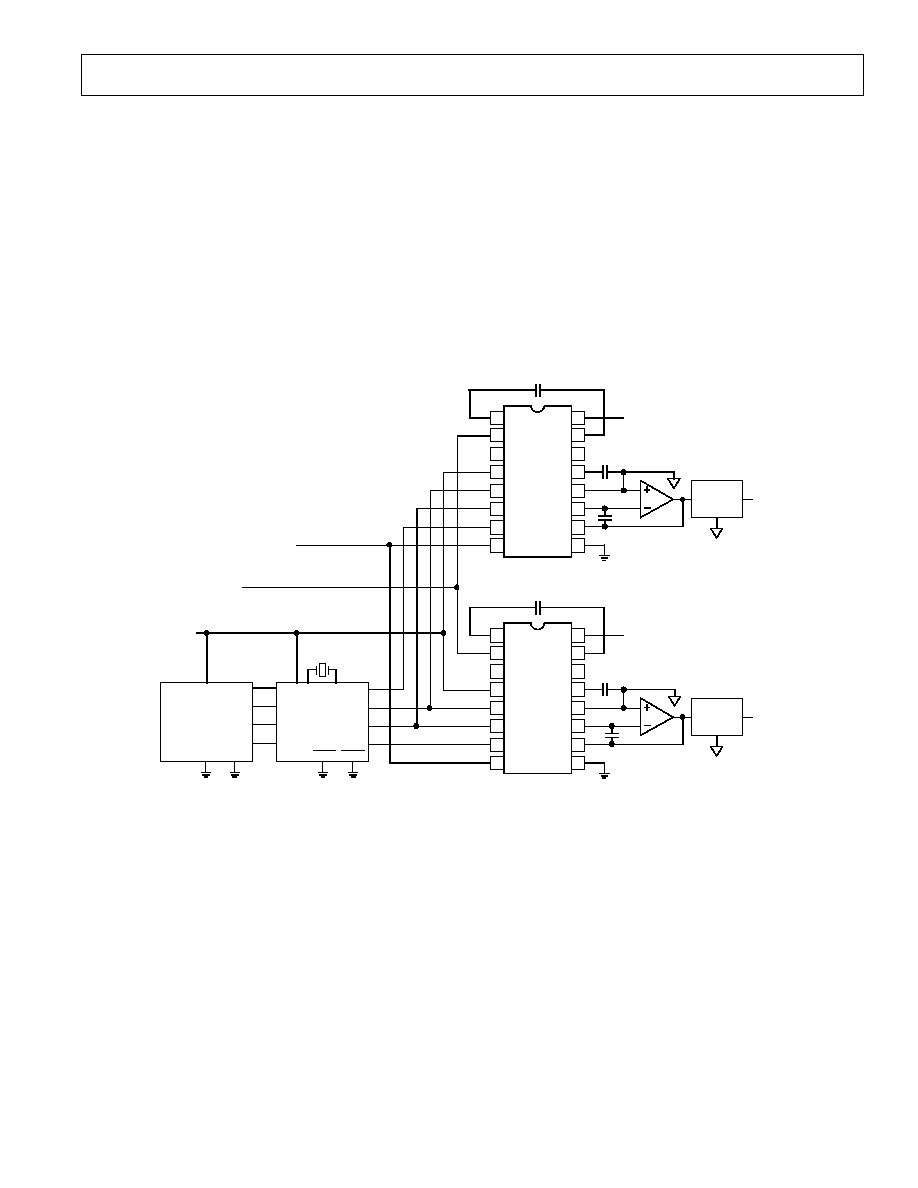
DIGITAL CIRCUIT CONSIDERATIONS
INPUT DATA
Data is transmitted to the AD1862 in a bit stream composed of
20-bit words with a serial, 2s complement, MSB first format.
Three signals must be present to achieve proper operation. They
are the data, clock and latch enable signals. Input data bits are
clocked into the input register on the rising edge of the clock
signal (CLK). The LSB is clocked in on the 20th clock pulse.
When all data bits are loaded, a low going latch enable (LE)
pulse updates the DAC input. Figure 12a illustrates the general
signal requirements for data transfer for the AD1862.
MSB
WORD n
LSB
MSB
WORD n+1
DATA
CLOCK
LATCH
ENABLE
Figure 12a. Input Data
TIMING
Figure 12b illustrates the specific timing requirements that must
be met in order for the data transfer to be accomplished success-
fully. The input pins of the AD1862 are both TTL and 5 V
CMOS compatible, independent of the power supplies used in
the application. The input requirements illustrated in Figure
12b are compatible with the data outputs provided by popular
digital interpolation filter chips used in digital audio playback
systems. The AD1862 input clock will run at 17 MHz allowing
data to be transferred at a rate of 16
◊
F
S
. Of course, it will also
function at slower rates such as 2
◊
, 4
◊
or 8
◊
F
S
.
>15ns
>15ns
BITS CLOCKED
TO SHIFT REGISTER
CLK
> 60ns
>15ns
>25ns
>25ns
DATA
LATCH ENABLE (LE)
>60ns
>40ns
INTERNAL DAC INPUT REGISTER
UPDATED WITH 20 MOST RECENT BITS
2nd BIT
LSB
(20th BIT)
WORD
NEXT
>40ns
>40ns
MSB
1st BIT
Figure 12b. Timing Requirements
AD1862
≠9≠
REV. A
The AD1862 is an extremely high performance DAC designed
for high-end consumer and professional digital audio applica-
tions. Compact disc players, digital preamplifiers, digital musi-
cal instruments and sound processors benefit from the extended
dynamic range, low THD+Noise and high signal-to-noise ratio.
For the first time, the D/A converter is no longer the basic limi-
tation in the performance of a CD player.
The performance of professional audio gear, such as mixing
consoles, digital tape recorders and multivoice synthesizers can
utilize the wide dynamic range and signal-to-noise ratio to
achieve greater performance. And, the AD1862's space saving
16-pin package contributes to compact system design. This per-
mits a system designer to incorporate more voices in multivoice
synthesizers, more tracks in multitrack tape recorders and more
channels in multichannel mixing consoles.
Furthermore, high-resolution signal processing and waveform
generation applications are equally well served by the AD1862.
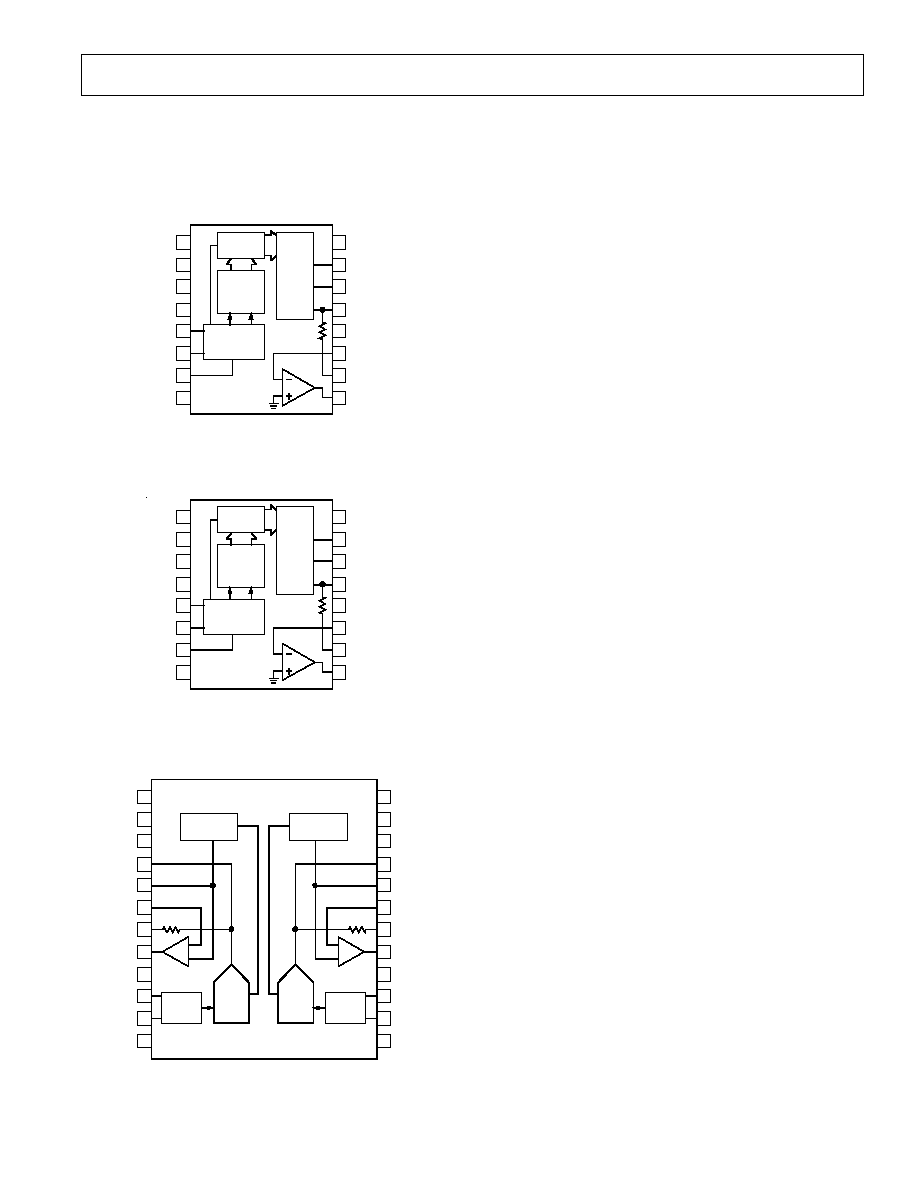
HIGH PERFORMANCE CD PLAYER
Figure 13 illustrates the application of AD1862s in a high per-
formance CD player. Two AD1862s are used, one for the left
channel and one for the right channel. The CXD11XX chip de-
codes the digital data coming from the read electronics and
sends it to the SM5813. Input data is sent to each AD1862 by
the SM5813 digital interpolating filter. This device operates at
8 times oversampling. The NE5534 op amps are chosen for
current-to-voltage converters due to their low distortion and low
noise. The output filters are 5-pole designs. For the purpose of
clarity, all bypass capacitors have been omitted from the schematic.
5V DIGITAL
SUPPLY
NE5534
LEFT
CHANNEL
OUTPUT
RIGHT
CHANNEL
OUTPUT
5V DIGITAL
SUPPLY
≠
16.9344MHz
XTI
XTO DOL
CKO
BCKO
WCKO
DOR
BCKI
DIN
LRCI
SM5813
XTAI
LRCK
DATA
C210
SLOB
PSSL
SONY
CXD1125
1130
1135
OW20 CKDV
LOW PASS
FILTER
10
µ
F
1
µ
F
12V ANALOG
SUPPLY
1
2
3
4
5
6
7
8
9
10
11
12
13
14
15
16
LOW PASS
FILTER
10
µ
F
1
µ
F
12V ANALOG
SUPPLY
1
2
3
4
5
6
7
8
9
10
11
12
13
14
15
16
12V ANALOG
SUPPLY
≠
NE5534
+
+
+
+
V
+
L
LE
V
≠
S
TRIM
CLK
DATA
V
≠
L
V
≠
S
V
+
S
NR
2
ADJ
NR
1
AGND
I
OUT
R
F
DGND
AD1862
AD1862
V
+
S
NR
2
ADJ
NR
1
AGND
I
OUT
R
F
DGND
V
+
L
LE
V
≠
S
TRIM
CLK
DATA
V
≠
L
V
≠
S
Figure 13. High Performance 20-Bit 8
◊
Oversampling CD Player Application

AD1862
≠10≠
REV. A
HIGH-RESOLUTION SIGNAL PROCESSING
Figure 14 illustrates the AD1862 combined with the DSP56000.
In high-resolution applications, the combination of the 24-bit
architecture of the DSP56000 and the low noise and high reso-
lution of the AD1862 can produce a high-resolution, low-noise
system.
As shown in Figure 14, the clock signal supplied by the DSP
processor must be inverted to be compatible with the input of
the AD1862. The exact architecture of the output low-pass filter
depends on the sample rate of the output data. In general, the
higher the oversampling rate, the fewer number of filter poles
are required to prevent aliasing.
The 20-bit resolution is particularly suitable for professional au-
dio, mixing or equalization equipment. Its resolution allows
24 dB of equalization to be performed on 16-bit input words
without signal truncation. Furthermore, up to sixteen 16-bit in-
put words can be mixed and output directly to the AD1862. In
this case, no loss of signal information would be encountered.
1
2
3
4
5
6
7
8
9
10
11
12
13
14
15
16
LOW PASS
FILTER
OUTPUT
VOLTAGE
0.1
µ
F
0.1
µ
F
0.1
µ
F
5V
DIGITAL
SUPPLY
≠
12V
ANALOG
SUPPLY
≠
12V
ANALOG
SUPPLY
0.1
µ
F
10
µ
F
AD846
ANALOG
COMMON
DIGITAL
COMMON
5V
DIGITAL
SUPPLY
V
CC
SCK
SC2
STD
V
DD
DSP56001
1
µ
F
AD1862
V
+
S
NR
2
ADJ
NR
1
AGND
I
OUT
R
F
DGND
V
+
L
LE
V
≠
S
TRIM
CLK
DATA
V
≠
L
V
≠
S
Figure 14. DSP56001 and AD1862 Produce High Resolution Signal Processing System
AD1862
≠11≠
REV. A
OTHER DIGITAL AUDIO COMPONENTS AVAILABLE
FROM ANALOG DEVICES
AD1856 16-Bit Audio DAC
Complete, No External Components Required
0.0025% THD
Low Cost
16-Pin DIP or SOIC Package
Standard Pinout
AD1860 18-Bit Audio DAC
Complete, No External Components Required
0.002% THD+N
108 dB Signal-to-Noise Ratio
16-Pin DIP or SOIC Package
AD1864 Dual 18-Bit Audio DAC
Complete, No External Components
0.002% THD+N
115 dB Channel Separation
24-Pin DIP
1
2
3
4
5
6
7
8
9
10
11
12
13
14
15
16
16-BIT
LATCH
16-BIT
DAC
SERIAL
INPUT
REGISTER
CONTROL
LOGIC
AD1856
I
OUT
V
S
≠
DGND
NC
CLK
LE
DATA
V
L
≠
V
L
+
NC NO CONNECT
=
V
S
+
TRIM
MSB ADJ
I
OUT
AGND
SJ
R
F
V
OUT
NC NO CONNECT
=
1
2
3
4
5
6
7
8
9
10
11
12
13
14
15
16
18-BIT
LATCH
18-BIT
DAC
SERIAL
INPUT
REGISTER
CONTROL
LOGIC
AD1860
I
OUT
V
S
≠
DGND
NC
CLK
LE
DATA
V
L
+
V
S
+
TRIM
MSB ADJ
I
OUT
AGND
SJ
R
F
V
OUT
V
L
≠
V
S
≠
1
2
3
4
5
6
7
8
9
10
11
12
TRIM
MSB
I
OUT
AGND
SJ
R
F
V
OUT
V
+
L
DR
LR
CK
18-BIT
LATCH
REFERENCE
20
18-BIT
LATCH
DGND
V
L
≠
V
S
+
TRIM
MSB
I
OUT
AGND
SJ
R
F
V
OUT
13
14
15
16
DL
LL
17
18
19
21
22
23
24
REFERENCE
18-BIT
DAC
18-BIT
DAC
AD1864
AD1862
≠12≠
REV. A
OUTLINE DIMENSIONS
Dimensions shown in inches and (mm).
C1445≠7≠9/90
PRINTED IN U.S.A.
Plastic DIP
(N-16)