Document Outline
- FEATURES
- ENHANCED FEATURES
- FUNCTIONAL BLOCK DIAGRAM
- SPECIFICATIONS
- TIMING PARAMETERS
- ABSOLUTE MAXIMUM RATINGS
- ENVIRONMENTAL CONDITIONS
- ORDERING GUIDE
- PIN CONFIGURATION
- PIN FUNCTION DESCRIPTIONS
- Indexed Control Registers
- Reset Register
- Master Volume Register
- Headphones Volume Register
- Mono Volume Register
- Phone_in Volume Register
- MIC Volume Register
- Line-In Volume Register
- CD Volume Register
- AUX Volume Register
- PCM-Out Volume Register
- Record Select Control Register
- Record Gain Register
- General-Purpose Register
- Audio Interrupt and Paging Mechanism Register
- Power-Down Control/Status Register
- Extended Audio ID Register
- Extended Audio Status and Control Register
- AC ê97 2.2 AMAP Compliant Default SPDIF Slot Assignments
- PCM Front DAC Rate Register
- PCM Surround DAC Rate Register
- PCM LFE (and CENTER) DAC Rate Register
- PCM ADC Rate Register
- CENTER/LFE Volume Control Register
- Surround Volume Control Register
- SPDIF Control Register
- Jack Sense/Audio Interrupt Status Register
- Serial Configuration Register
- Miscellaneous Control Bit Register
- Vendor ID Register
- Codec ID and Clock Selection Table
- OUTLINE DIMENSIONS

a
AD1888
AC '97 SoundMAX
Æ
Codec
REV. 0
One Technology Way, P.O. Box 9106, Norwood, MA 02062-9106, U.S.A.
Tel: 781/329-4700
www.analog.com
Fax: 781/326-8703
© 2003 Analog Devices, Inc. All rights reserved.
Information furnished by Analog Devices is believed to be accurate and
reliable. However, no responsibility is assumed by Analog Devices for its
use, nor for any infringements of patents or other rights of third parties that
may result from its use. No license is granted by implication or otherwise
under any patent or patent rights of Analog Devices. Trademarks and
registered trademarks are the property of their respective owners.
FEATURES
AC '97 2.3 COMPATIBLE FEATURES
6 DAC Channels for 5.1 Surround
90 dB Dynamic Range
20-Bit PCM DACs
S/PDIF Output
Integrated Stereo Headphone Amplifiers
Phone, Aux, and Line-In
High Quality CD Input
Selectable MIC Input
Mono Output
External Amplifier Power-Down Control
Double Rate Audio (f
S
= 96 kHz)
Power Management Modes
48-Lead LQFP and 48-Lead LFCSP Packages
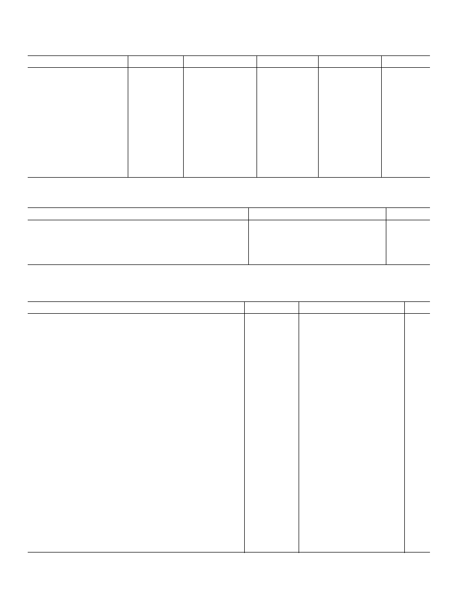
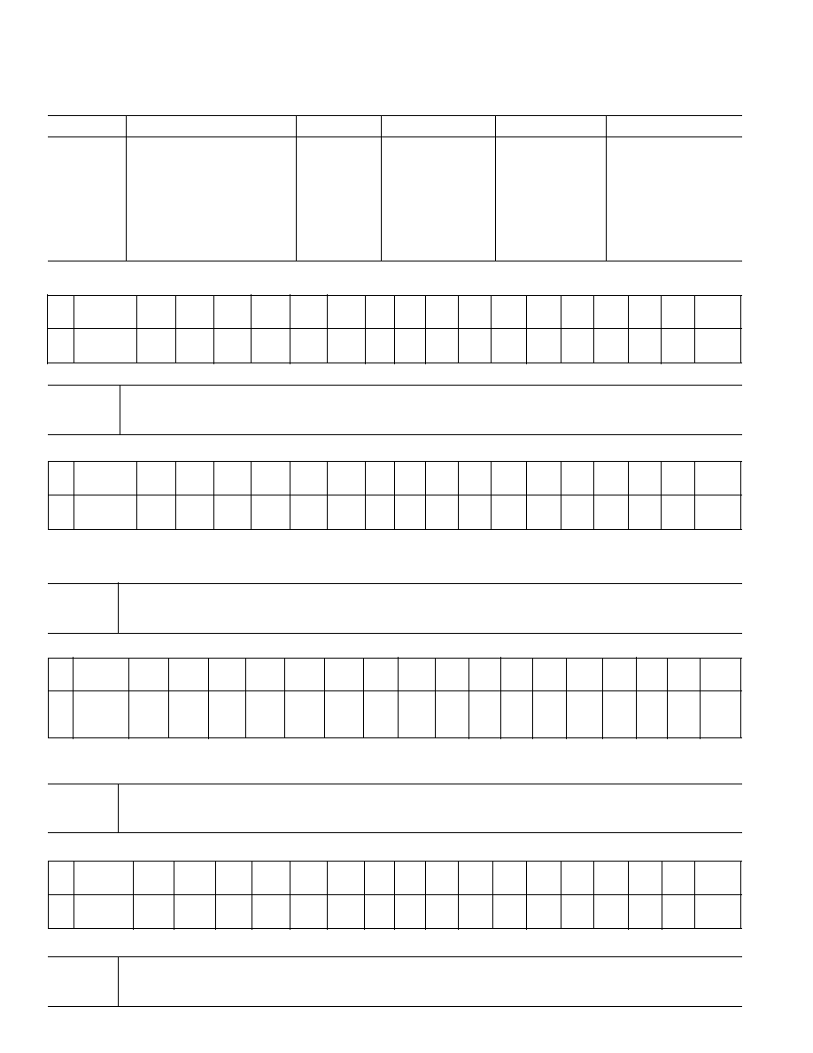
FUNCTIONAL BLOCK DIAGRAM
ID0
ID1
RESET
SYNC
BIT_CLK
SDATA_OUT
SDATA_IN
SPDIF_OUT
EAPD
JS0
JS1
V
REF
V
REFOUT
AC '97
CONTROL
REGISTERS
DAC
SLOT
LOGIC
G = GAIN
A = ATTENUATION
M = MUTE
Z = HIGH-Z
M
A
MONO_OUT
M
GA
M
16-BIT -
ADC
G
M
G
M
M
M
M
M
M
M
GA
M
GA
M
GA
M
GA
M
GA
M
GA
M
GA
M
GA
M
GA
M
GA
M
GA
M
GA
M
GA
ADC
SLOT
LOGIC
PLL
AC '97 INTERFACE
SPDIF
TX
EAPD
JACK
SENSE
LOGIC
VOLTAGE
REFERENCE
M
A
SURR_L/
HP_OUT_L
HP
M
A
SURR_R/
HP_OUT_R
HP
MZ
A
LFE_OUT
MZ
A
CENTER_OUT
MZ
A
LINE_OUT_R
MZ
A
LINE_OUT_L
16-BIT -
ADC
PHONE_IN
CD_L
CD_R
AUX_L
AUX_R
LINE_IN_L
LINE_IN_R
MIC1
MIC2
XTAL_IN
AD1888
XTAL_OUT
20-BIT -
DAC
20-BIT -
DAC
20-BIT -
DAC
20-BIT -
DAC
20-BIT -
DAC
20-BIT -
DAC
M
GA
G
DIFF
AMP
ENHANCED FEATURES
Selectable Front and Rear MIC Inputs
with Preamp
Integrated PLL for System Clocking
Crystal-Free Operation
Variable Sample Rate 7 kHz to 96 kHz
Jack Sense (Auto Topology Switching)
Software Controlled VREF_OUT for MIC Bias
Software Enabled Outputs for Jack Sharing
Auto Down-Mix and Channel Spreading Modes

REV. 0
≠2≠
AD1888≠SPECIFICATIONS
Parameter
Min
Typ
Max
Unit
ANALOG INPUT
Input Voltage (RMS Values Assume Sine Wave Input)
LINE_IN, CD, AUX, PHONE_IN
1
V rms
2.83
V p-p
MIC_IN with 30 dB Preamp
0.032
V rms
0.089
V p-p
MIC_IN with 20 dB Preamp
0.1
V rms
0.283
V p-p
MIC_IN with 10 dB Preamp
0.316
V rms
0.894
V p-p
MIC_IN with 0 dB Gain
1
V rms
2.83
V p-p
Input Impedance
*
20
k
Input Capacitance
*
5
7.5
pF
MASTER VOLUME
Step Size (Line Out, Mono Out, Surround Out, Center, LFE)
1.5
dB
Output Attenuation Range Span
*
46.5
dB
Mute Attenuation of 0 dB Fundamental
*
80
dB
PROGRAMMABLE GAIN AMPLIFIER--ADC
Step Size (0 dB to 22.5 dB)
1.5
dB
PGA Gain Range Span
22.5
dB
ANALOG MIXER--INPUT GAIN/AMPLIFIERS/ATTENUATORS
Signal-to-Noise Ratio (SNR)
CD to LINE_OUT
90
dB
LINE, AUX, or PHONE to LINE_OUT
*
90
dB
MIC1 or MIC2 (Note: MIC Gain of 0 dB) to LINE_OUT
*
90
dB
Step Size All Mixer Inputs
1.5
dB
Input Gain/Attenuation Range: All Mixer Inputs
46.5
dB
DIGITAL DECIMATION AND INTERPOLATION FILTERS
*
Pass Band
0
0.4 f
S
Hz
Pass-Band Ripple
±0.09
dB
Transition Band
0.4 f
S
0.6 f
S
Hz
Stop Band
0.6 f
S
Hz
Stop-Band Rejection
≠74
dB
Group Delay
16/f
S
sec
Group Delay Variation over Pass Band
0
µs
STANDARD TEST CONDITIONS, UNLESS OTHERWISE
NOTED
Temperature
25
∞C
Digital Supply (DV
DD
)
3.3 V
Analog Supply (AV
DD
)
5.0 V
Sample Rate (f
S
)
48 kHz
Input Signal
1 kHz
Analog Output Pass Band
20 Hz to 20 kHz
DAC Test Conditions
Calibrated
≠3 dB Attenuation Relative to Full Scale
0 dB Input
10 k
Output Load LINE_OUT, MONO_OUT,
CENTER_OUT, and LFE_OUT
32
Output Load (HP_OUT)
ADC Test Conditions
Calibrated
0 dB Gain
Input ≠3.0 dB Relative to Full Scale

REV. 0
AD1888
≠3≠
Parameter
Min
Typ
Max
Unit
ANALOG-TO-DIGITAL CONVERTERS
Resolution
16
Bits
Total Harmonic Distortion (THD) AV
DD
= 5.0 V
≠78
dB
Dynamic Range (≠60 dB Input THD + N Referenced to FS, A-Weighted)
AV
DD
= 5.0 V
80
dB
Signal-to-Intermodulation Distortion
* (CCIF Method)
84
dB
ADC Crosstalk
*
Line Inputs (Input L, Ground R, Read R; Input R, Ground L, Read L)
≠85
dB
LINE_IN to Other
≠85
dB
Gain Error (Full-Scale Span Relative to Nominal Input Voltage)
±10
%
Interchannel Gain Mismatch (Difference of Gain Errors)
±0.5
dB
ADC Offset Error
*
(0 dB Gain, HPF On)
±10
mV
DIGITAL-TO-ANALOG CONVERTERS
Resolution
20
Bits
Total Harmonic Distortion (THD), LINE_OUT, AV
DD
= 5.0 V
≠80
dB
Total Harmonic Distortion (THD), HP_OUT, AV
DD
= 5.0 V
≠70
dB
Total Harmonic Distortion (THD), CENTER/LFE, AV
DD
= 5.0 V
≠80
dB
Dynamic Range (≠60 dB Input THD + N Referenced to FS A-Weighted)
AV
DD
= 5.0 V, All Outputs
90
dB
Signal-to-Intermodulation Distortion
* (CCIF Method)
88
dB
Gain Error (Full-Scale Span Relative to Nominal Input Voltage)
±10
%
Interchannel Gain Mismatch (Difference of Gain Errors)
±0.7
dB
DAC Crosstalk (Input L, Zero R, Read LINE_OUT_R; Input R,
≠80
dB
Zero L, Read LINE_OUT_L, 10 k
Load)*
Total Audible Out-of-Band Energy
* (Measured from 0.6 f
S
to 20 kHz)
≠40
dB
ANALOG OUTPUT
Full-Scale Output Voltage; LINE_OUT/MONO_OUT, CENTER_OUT,
LFE_OUT
1
V rms
2.83
V p-p
Output Impedance
*
300
External Load Impedance
*
(LINE_OUT, CENTER_OUT/LFE_OUT,
MONO_OUT)
10
k
Output Capacitance
*
15
pF
External Load Capacitance
*
100
pF
Full-Scale Output Voltage; HP_OUT (0 dB Gain)
1
V rms
External Load Impedance
*; HP_OUT
32
V
REF
2.05
2.25
2.45
V
V
REF_OUT
(V
REFH
= 0)
2.25
V
V
REF_OUT
(V
REFH
= 1)
3.65
V
V
REF_OUT
Current Drive
5
mA
Mute Click (Muted Output Minus Unmuted Midscale DAC Output)
±5
mV
STATIC DIGITAL SPECIFICATIONS
High Level Input Voltage (V
IH
): Digital Inputs
0.65
DV
DD
V
Low Level Input Voltage (V
IL
)
0.35
DV
DD
V
High Level Output Voltage (V
OH
), I
OH
= 2 mA
0.9 DV
DD
V
Low Level Output Voltage (V
OL
), I
OL
= 2 mA
0.1 DV
DD
V
Input Leakage Current
≠10
+10
µA
Output Leakage Current
≠10
+10
µA
POWER SUPPLY
Power Supply Range, Analog (AV
DD
)
4.75
5.25
V
Power Supply Range, Digital (DV
DD
)
3.15
3.45
V
Power Dissipation 5 V/3.3 V
563
mW
Analog Supply Current 5 V (AV
DD
)
70
mA
Digital Supply Current 3.3 V (DV
DD
)
53
mA
Power Supply Rejection (100 mV p-p Signal @ 1 kHz)
*
(At Both Analog and Digital Supply Pins, Both ADCs and DACs)
≠40
dB
*Guaranteed but not tested.
Specifications subject to change without notice.
REV. 0
≠4≠
AD1888
Parameter
PR[K:I]
1
PR[6:0]
1
DV
DD
Typ
AV
DD
Typ
Unit
POWER-DOWN STATES
2
Fully Active
000
000 0000
53
70
mA
ADC
000
000 0001
44
66
mA
FRONT DAC
000
000 0010
46
61
mA
SURROUND DAC
010
000 0000
46
61
mA
CENTER/LFE DAC
101
000 0000
46
61
mA
ADC + ALL DACs
111
000 0011
12
33
mA
Mixer
000
000 0100
52
44
mA
ADC + Mixer
000
000 0101
45
39
mA
ALL DACs + Mixer
111
000 0110
31
14
mA
ADC + ALL DACs + Mixer
111
000 0111
12
8
mA
Standby
111
011 1111
0
0
mA
Headphone Standby
000
100 0000
52
65
mA
NOTES
1
PR bits are controlled in Reg. 2Ah and 26h
2
Values presented with V
REFOUT
loaded.
Specifications subject to change without notice.
Parameter
Symbol
Min
Typ
Max
Unit
RESET Active Low Pulse Width
t
RST_LOW
1.0
µs
RESET Inactive to BIT_CLK Startup Delay
t
RST2CLK
162.8
400,000
ns
SYNC Active High Pulse Width
t
SYNC_HIGH
1.3
µs
SYNC Low Pulse Width
t
SYNC_LOW
19.5
µs
SYNC Inactive to BIT_CLK Startup Delay
t
SYNC2CLK
162.8
ns
BIT_CLK Frequency
12.288
MHz
BIT_CLK Frequency Accuracy
1.0
ppm
BIT_CLK Period
t
CLK_PERIOD
81.4
ns
BIT_CLK Output Jitter
1, 2
750
ps
BIT_CLK High Pulse Width
t
CLK_HIGH
40
41.7
ns
BIT_CLK Low Pulse Width
t
CLK_LOW
39.7
41.4
ns
SYNC Frequency
48.0
kHz
SYNC Period
t
SYNC_PERIOD
20.8
µs
Setup to Falling Edge of BIT_CLK
t
SETUP
4
ns
Hold from Falling Edge of BIT_CLK
t
HOLD
3
ns
BIT_CLK Rise Time
t
RISECLK
2
4
6
ns
BIT_CLK Fall Time
t
FALLCLK
2
4
6
ns
SYNC Rise Time
t
RISESYNC
2
4
6
ns
SYNC Fall Time
t
FALLSYNC
2
4
6
ns
SDATA_IN Rise Time
t
RISEDIN
2
4
6
ns
SDATA_IN Fall Time
t
FALLDIN
2
4
6
ns
SDATA_OUT Rise Time
t
RISEDOUT
2
4
6
ns
SDATA_OUT Fall Time
t
FALLDOUT
2
4
6
ns
End of Slot 2 to BIT_CLK, SDATA_IN Low
t
S2_PDOWN
0
1.0
µs
Setup to RESET Inactive (SYNC, SDATA_OUT)
t
SETUP2RST
15
ns
Rising Edge of RESET to Hi-Z Delay
t
OFF
25
ns
Propagation Delay
15
ns
RESET Rise Time
50
ns
Output Valid Delay from BIT_CLK Rising
15
ns
NOTES
1
Guaranteed but not tested.
2
Output jitter directly dependent on crystal input jitter.
Specifications subject to change without notice.
TIMING PARAMETERS
(Guaranteed over Operating Temperature Range)
Parameter
Min
Typ
Max
Unit
CLOCK SPECIFICATIONS
*
Input Clock Frequency (XTAL Mode or Clock Oscillator)
24.576
MHz
Input Clock Frequency (Reference Clock Mode)
14.31818
MHz
Input Clock Frequency (USB Clock Mode)
48.000
MHz
Recommended Clock Duty Cycle
40
50
60
%
*Guaranteed but not tested.
Specifications subject to change without notice.
REV. 0
AD1888
≠5≠
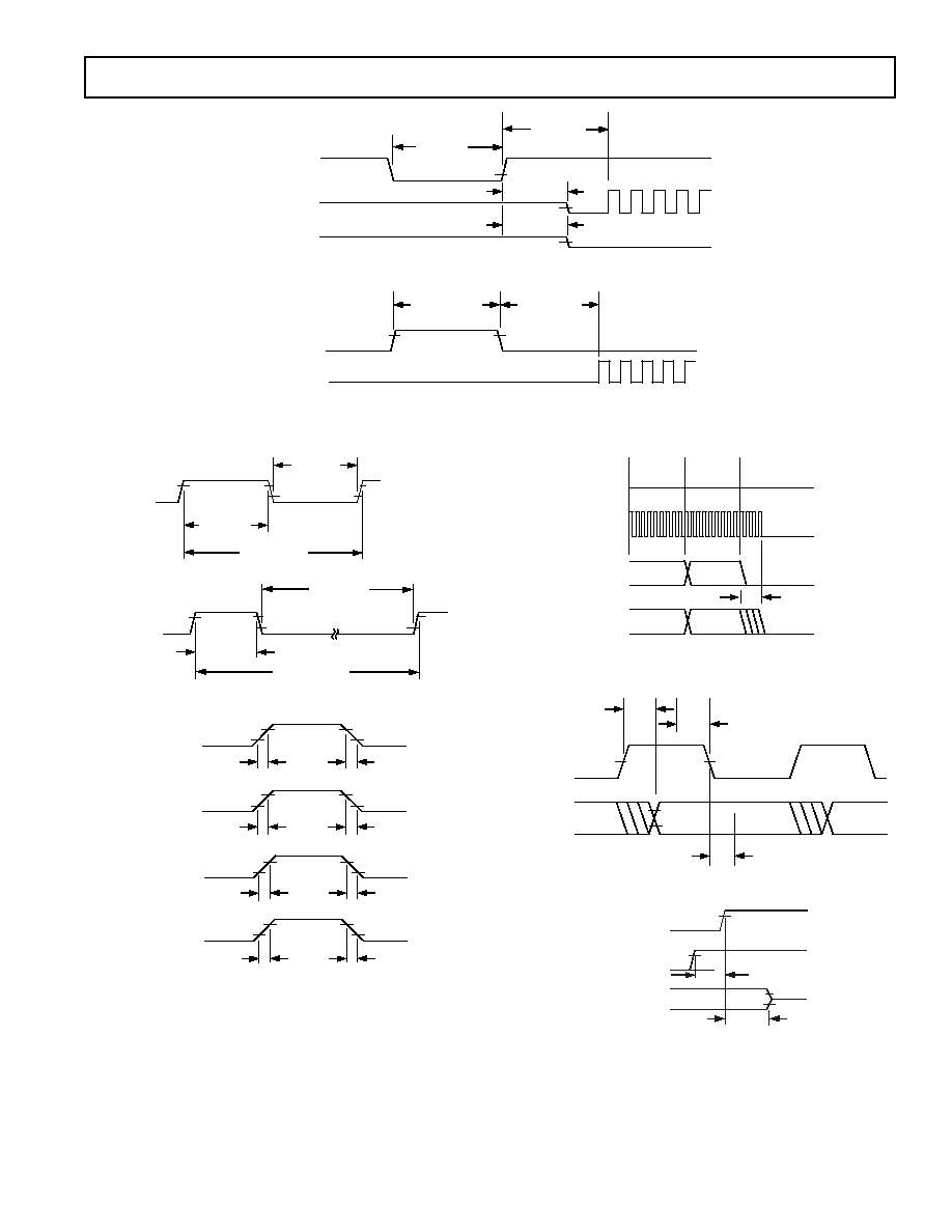
RESET
BIT_CLK
SDATA_IN
t
RST_LOW
t
RST2CLK
t
TRI2ACTV
t
TRI2ACTV
Figure 1. Cold Reset Timing (Codec is Supplying the Bit_CLK Signal)
SYNC
BIT_CLK
t
SYNC_HIGH
t
SYNC2CLK
Figure 2. Warm Reset Timing
BIT_CLK
SYNC
t
CLK_LOW
t
CLK_HIGH
t
CLK_PERIOD
t
SYNC_LOW
t
SYNC_PERIOD
t
SYNC_HIGH
Figure 3. Clock Timing
BIT_CLK
SYNC
SDATA_IN
SDATA_OUT
t
RISECLK
t
FALLCLK
t
RISESYNC
t
FALLSYNC
t
RISEDIN
t
FALLDIN
t
RISEDOUT
t
FALLDOUT
Figure 4. Signal Rise and Fall Times
BIT_CLK
SYNC
SDATA_IN
SDATA_OUT
BIT_CLK NOT TO SCALE
SLOT 1
SLOT 2
WRITE TO
0x26
DATA
PR4
t
S2_PDOWN
Figure 5. AC-Link Low Power Mode Timing
BIT_CLK
SDATA_OUT
SDATA_IN
SYNC
t
CO
t
SETUP
V
IH
V
IL
V
OH
V
OL
t
HOLD
Figure 6. AC-Link Low Power Mode Timing
RESET
SDATA_OUT
SDATA_IN, BIT_CLK,
EAPD, SPDIF_OUT
AND DIGITAL I/O
Hi-Z
t
SETUP2RST
t
OFF
Figure 7. ATE Test Mode
REV. 0
≠6≠
AD1888
ABSOLUTE MAXIMUM RATINGS
*
Parameter
Min
Max
Unit
Power Supplies
Digital (DV
DD
)
≠0.3
+3.6
V
Analog (AV
DD
)
≠0.3
+6.0
V
Input Current (Except Supply Pins)
±10.0
mA
Analog Input Voltage (Signal Pins)
≠0.3
AV
DD
+ 0.3
V
Digital Input Voltage (Signal Pins)
≠0.3
DV
DD
+ 0.3 V
Ambient Temperature (Operating)
0
+70
∞C
Storage Temperature
≠65
+150
∞C
*Stresses greater than those listed under Absolute Maximum Ratings may cause
permanent damage to the device. This is a stress rating only and functional
operation of the device at these or any other conditions above those indicated in
the operational section of this specification is not implied. Exposure to absolute
maximum rating conditions for extended periods may affect device reliability.
ENVIRONMENTAL CONDITIONS
*
Ambient Temperature Rating
TCASE = Case Temperature in
∞C
PD = Power Dissipation in W
JA
= Thermal Resistance (Junction-to-Ambient)
JC
= Thermal Resistance (Junction-to-Case)
CAUTION
ESD (electrostatic discharge) sensitive device. Electrostatic charges as high as 4000 V readily
accumulate on the human body and test equipment and can discharge without detection. Although the
AD1888 features proprietary ESD protection circuitry, permanent damage may occur on devices
subjected to high energy electrostatic discharges. Therefore, proper ESD precautions are recommended
to avoid performance degradation or loss of functionality.
Package
JA
JC
LQFP
50.1
∞C/W
17.8
∞C/W
LFCSP
50
∞C/W
25.88
∞C/W
*All measurements per EIA/JESD51 with 2S2P
test board per EIA/JESD51-7.
ORDERING GUIDE
Model
Temperature Range
Package Description
Package Option
AD1888JST
0
∞C to 70∞C
48-Lead LQFP, Tray Version
ST-48
AD1888JST-REEL
0
∞C to 70∞C
48-Lead LQFP, Reel Version
ST-48
AD1888JSTZ
*
0
∞C to 70∞C
48-Lead LQFP, Tray Version
ST-48
AD1888JSTZ-REEL
*
0
∞C to 70∞C
48-Lead LQFP, Reel Version
ST-48
AD1888JCP
0
∞C to 70∞C
48-Lead LFCSP, Tray Version
CP-48
AD1888JCP-REEL
0
∞C to 70∞C
48-Lead LFCSP, Reel Version
CP-48
*Z = Lead Free

REV. 0
AD1888
≠7≠
PIN FUNCTION DESCRIPTIONS
Pin Number
Mnemonic
I/O
Function
DIGITAL INPUT/OUTPUT
2
XTL_IN
I
Crystal Input (24.576 MHz) or External Clock In (24.576 MHz,
14.31818 MHz, or 48000 MHz).
3
XTL_OUT
O
Crystal Output.
5
SDATA_OUT
I
AC-Link Serial Data Output. AD1888 input stream.
6
BIT_CLK
O/I
AC-Link Bit Clock. 12.288 MHz serial data clock. (Input pin for
Secondary mode only.)
8
SDATA_IN
O
AC-Link Serial Data Input. AD1888 output stream.
10
SYNC
I
AC-Link Frame Sync.
11
RESET
I
AC-Link Reset. AD1888 master H/W reset.
48 SPDIF O SPDIF
Output.
CHIP SELECTS/CLOCK STRAPPING
45
ID0
I
Chip Select Input 0 (Active Low).
46
ID1
I
Chip Select Input 1 (Active Low).
JACK SENSE AND EAPD
47
EAPD
O
EAPD Output.
17
JS0
I
Jack Sense 0 Input.
16
JS1
I
Jack Sense 1 Input.
PIN CONFIGURATION
48-Lead LQFP
1
2
3
4
5
6
7
8
9
10
11
12
DV
DD
1
XTL_IN
XTL_OUT
DV
SS
1
SDATA_OUT
BIT_CLK
DV
SS
2
SDATA_IN
DV
DD
2
SYNC
RESET
NC
36
35
34
33
32
31
30
29
28
27
26
25
LINE_OUT_R (FRONT_R)
LINE_OUT_L (FRONT_L)
AV
DD
4
AV
SS
4
LFE_OUT
CENTER_OUT
AFILT2
AFILT1
V
REFOUT
V
REF
AV
SS
1
AV
DD
1
13
14
15
16
17
18
19
20
21
22
23
24
PHONE_IN
AUX_L
AUX_R
JS1
JS0
CD_L
CD_GND_REF
CD_R
MIC1
MIC2
LINE_IN_L
LINE_IN_R
48
47
46
45
44
43
42
41
40
39
38
37
SPDIF
EAPD
ID1
ID0
AV
SS
3
AV
DD
3
NC
SURR_OUT_R/HP_OUT_R
AV
SS
2
SURR_OUT_L/HP_OUT_L
AV
DD
2
MONO_OUT
AD1888
TOP VIEW
(Not to Scale)
NC = NO CONNECT

REV. 0
≠8≠
AD1888
Pin Number
Mnemonic
I/O
Function
ANALOG INPUT/OUTPUT
13
PHONE_IN
I
Monaural Line-Level Input.
14
AUX_L
I
Auxiliary Input, Left Channel.
15
AUX_R
I
Auxiliary Input, Right Channel.
18
CD_L
I
CD Audio Left Channel.
19
CD_GND_REF
I
CD Audio Analog Ground Reference for Differential CD Input.
20
CD_ R
I
CD Audio Right Channel.
21
MIC1
I
Rear Panel MIC Input.
22
MIC2
I
Front Panel MIC Input.
23
LINE_IN_L
I
Line-In Left Channel.
24
LINE_IN_R
I
Line-In Right Channel.
31
CENTER_OUT
O
Center Channel Output.
32
LFE_OUT
O
Low Frequency Enhanced Output.
35
LINE_OUT_L
O
Line Out (Front) Left Channel.
36
LINE_OUT_R
O
Line Out (Front) Right Channel.
37
MONO_OUT
O
Monaural Output to Telephone Subsystem Speakerphone.
39
SURR_OUT_L/HP_OUT_L
O
Surround Front Headphone Left Channel Output.
41
SURR_OUT_R/HP_OUT_R
O
Surround Front Headphone Right Channel Output.
FILTER/REFERENCE
27
V
REF
O
Voltage Reference Filter.
28
V
REFOUT
O
Voltage Reference Output 5 mA Drive (intended for MIC bias).
29
AFILT1
O
Antialiasing Filter Capacitor--ADC Right Channel.
30
AFILT2
O
Antialiasing Filter Capacitor--ADC Left Channel.
POWER AND GROUND SIGNALS
1
DV
DD
1
I
Digital V
DD
3.3 V.
4
DV
SS
1
I
Digital GND.
7
DV
SS
2
I
Digital GND.
9
DV
DD
2
I
Digital V
DD
3.3 V.
25
AV
DD
1
I
Analog V
DD
5.0 V.
26
AV
SS
1
I
Analog GND.
33
AV
SS
4
I
Analog GND.
34
AV
DD
4
I
Analog V
DD
5.0 V.
38
AV
DD
2
I
Analog V
DD
5.0 V.
40
AV
SS
2
I
Analog GND.
43
AV
DD
3
I
Analog V
DD
5.0 V.
44
AV
SS
3
I
Analog GND.
NO CONNECTS
12
NC
No Connect.
42
NC
No Connect.

REV. 0
AD1888
≠9≠
Indexed Control Registers
Reg Name
D15
D14
D13
D12
D11
D10
D9
D8
D7
D6
D5
D4
D3
D2
D1
D0
Default
00h Reset
X
SE4
SE3
SE2
SE1
SE0
ID9
ID8
ID7
ID6
ID5
ID4
ID3
ID2
ID1
ID0
0090h
02h Master Volume
MM
X
LMV5
LMV4
LMV3
LMV2
LMV1
LMV0
MMRM
* X
RMV5 RMV4 RMV3 RMV2 RMV1 RMV0
8000h
04h Headphone
HPM
X
LHV5
LHV4
LHV3
LHV2
LHV1
LHV0
HPRM
*
X
RHV5
RHV4
RHV3
RHV2
RHV1
RHV0
8000h
Volume
06h Mono Volume
MVM
X
X
X
X
X
X
X
X
X
MV5
MV4
MV2
MV2
MV1
MV0
8000h
0Ch Phone Volume
PHM
X
X
X
X
X
X
X
X
X
X
PHV4
PHV3
PHV2
PHV1
PHV0
8008h
0Eh MIC Volume
MCM
X
X
X
X
X
X
X
X
M20
X
MCV4 MCV3 MCV2 MCV1 MCV0
8008h
10h Line-In Volume
LVM
X
X
LLV4
LLV3
LLV2
LLV1
LLV0
LVRM
*
X
X
RLV4
RLV3
RLV2
RLV1
RLV0
8808h
12h CD Volume
CVM
X
X
LCV4
LCV3
LCV2
LCV1
LCV0
CDRM
*
X
X
RCV4
RCV3
RCV2
RCV1
RCV0
8808h
16h AUX Volume
AVM
X
X
LAV4
LAV3
LAV2
LAV1
LAV0
AVRM
*
X
X
RAV4
RAV3
RAV2
RAV1
RAV0
8808h
18h PCM Out Vol
OM
X
X
LOV4
LOV3
LOV2
LOV1
LOV0
OMRM
* X
X
ROV4
ROV3
ROV2
ROV1
ROV0
8808h
1Ah Record Select
X
X
X
X
X
LS2
LS1
LS0
X
X
X
X
X
RS2
RS1
RS0
0000h
1Ch Record Gain
IM
X
X
X
LIM3
LIM2
LIM1
LIM0
IMRM
*
X
X
X
RIM3
RIM2
RIM1
RIM0
8000h
20h General-Purpose X
X
X
X
DRSS1
DRSS0
X
MS
LPBK
X
X
X
X
X
X
X
0000h
24h Audio Int.
I4
X
X
X
I0
X
X
X
X
X
X
X
PG3
PG2
PG1
PG0
xxxxh
and Paging
26h Power-Down
EAPD
PR6
PR5
PR4
PR3
PR2
PR1
PR0
X
X
X
X
REF
ANL
DAC
ADC
NA
Ctrl/Stat
28h Ext'd Audio ID
ID1
ID0
X
X
REV1
REV0
AMAP LDAC
SDAC
CDAC
DSA1
DSA0
X
SPDIF DRA
VRA
x3C7h
2Ah Ext'd Audio
VFORCE X
PRK
PRJ
PRI
SPCV
X
ELDAC
ESDAC
ECDAC
SPSA1 SPSA0 X
ESPDIF EDRA
EVRA
0xx0h
Stat/Ctrl
2Ch PCM Front
SRF15
SRF14
SRF13
SRF12
SRF11
SRF10
SRF9
SRF8
SRF7
SRF6
SRF5
SRF4
SRF3
SRF2
SRF1
SRF0
BB80h
DAC Rate
2Eh PCM Surr
SRS15
SRS14
SRS13
SRS12
SRS11
SRS10
SRS9
SRS8
SRS7
SRS6
SRS5
SRS4
SRS3
SRS2
SRS1
SRS0
BB80h
DAC Rate
30h PCM C/LFE
SRCL15
SRCL14 SRCL13 SRCL12 SRCL11 SRCL10 SRCL9 SRCL8
SRCL7
SRCL6
SRCL5 SRCL4 SRCL3 SRCL2 SRCL1 SRCL0
BB80h
DAC Rate
32h PCM L/R
SRA15
SRA14
SRA13
SRA13
SRA11
SRA10
SRA9
SRA8
SRA7
SRA6
SRA5
SRA4
SRA3
SRA2
SRA1
SRA0
BB80h
ADC Rate
36h Center/LFE
LM
X
LFE5
LFE4
LFE3
LFE2
LFE1
LFE0
CM
X
CNT5
CNT4
CNT3
CNT2
CNT1
CNT0
8080h
Volume
38h Surround Volume MUTE_L X
LSR5
LSR4
LSR3
LSR2
LSR1
LSR0
MUTE_R X
RSR5
RSR4
RSR3
RSR2
RSR1
RSR0
8080h
3Ah SPDIF Control
V
X
SPSR1
SPSR0
L
CC6
CC5
CC4
CC3
CC2
CC1
CC0
PRE
COPY
/AUD
PRO
2000h
72h JACK SENSE
JS1
JS1
JS0
JS
JS
JS
X
X
JS1
JS0
JS1
JS0
JS1
JS0
JS1
JS0
0000h
SPRD
DMX
DMX
MT2
MT1
MT0
TMR
TMR
MD
MD
ST
ST
INT
INT
74h Serial
SLOT 16 REGM2 REGM1 REGM0 REGM3 DRF
X
CHEN
X
LBKS1
LBKS0 INTS
X
SPAL
SPDZ
SPLNK
1001h
Configuration
76h Misc Control
DACZ
AC97NC MSPLT LODIS
CLDIS
HPSEL
DMIX1 DMIX0 SPRD
X
LOSEL SRU
VREFH VREFD MBG1 MBG0
0000h
Bits
7Ch Vendor ID1
F7
F6
F5
F4
F3
F2
F1
F0
S7
S6
S5
S4
S3
S2
S1
S0
4144h
7Eh Vendor ID2
T7
T6
T5
T4
T3
T2
T1
T0
REV7
REV6
REV5
REV4
REV3
REV2
REV1
REV0
5368h
NOTES
All registers not shown and bits containing an X are assumed to be reserved.
Odd register addresses are aliased to the next lower even address.
Reserved registers should not be written to.
Zeros should be written to reserved bits.
*For AC '97 compatibility, Bit D7 is only available by setting the MSPLT bit, Register 76h. The MSPLT bit enables separate mute bits for the left and right
channels. If MSPLT is not set, Bit D7 has no effect.
REV. 0
≠10≠
AD1888
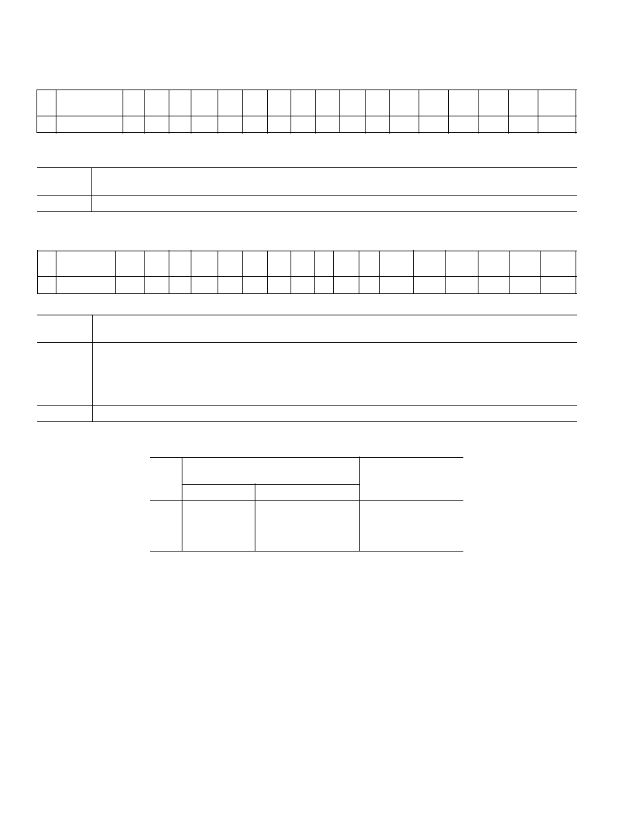
Master Volume Register (Index 02h)
Reg
No.
Name
D15
D14 D13
1
D12
D11
D10
D9
D8
D7
D6 D5
1
D4
D3
D2
D1
D0
Default
02h
Master
MM
X
LMV5
LMV4
LMV3
LMV2
LMV1 LMV0 MMRM
2
X
RMV5 RMV4 RMV3 RMV2
RMV1 RMV0 8000h
Volume
NOTES
1
Refer to Table I for examples. This register controls the Line_Out volume controls for both stereo channels and mute bit. Each volume subregister contains five bits,
generating 32 volume levels with 31 steps of 1.5 dB each. Because AC '97 defines 6-bit volume registers, to maintain compatibility whenever the D5 or D13 bits are
set to 1, their respective lower five volume bits are automatically set to 1 by the codec logic. On readback, all lower five bits will read 1s whenever these bits are set to 1.
2
For AC '97 compatibility, Bit D7 is available only by setting the MSPLT bit, Register 76h. The MSPLT bit enables separate mute bits for the left and right channels.
If MSPLT is not set, Bit D7 has no effect. All registers not shown and bits containing an X are assumed to be reserved.
Note that depending on the state of the AC97NC bit in Register 0x76, this register has the following additional functionality:
For AC97NC = 0, the register controls the Line_out output Attenuators only.
For AC97NC = 1, the register controls the Line_out, Center, and LFE output Attenuators.
Reset Register (Index 00h)
Reg
No.
Name
D15
D14
D13
D12
D11
D10
D9
D8
D7
D6
D5
D4
D3
D2
D1
D0
Default
00h
Reset
X
SE4
SE3
SE2
SE1
SE0
ID9
ID8
ID7
ID6
ID5
ID4
ID3
ID2
ID1
ID0
0090h
NOTES
All registers not shown and bits containing an X are assumed to be reserved.
Writing any value to this register performs a register reset, which causes all registers to revert to their default values (except 74h, which forces the serial configuration).
Reading this register returns the ID code of the part and a code for the type of 3D Stereo Enhancement.
ID[9:0] Identify Capability. The ID decodes the capabilities of AD1888 based on the following:
Bit = 1
Function
AD1888
ID0
Dedicated Mic PCM In Channel
0
ID1
Modem Line Codec Support
0
ID2
Bass and Treble Control
0
ID3
Simulated Stereo (Mono to Stereo)
0
ID4
Headphone Out Support
1
ID5
Loudness (Bass Boost) Support
0
ID6
18-Bit DAC Resolution
0
ID7
20-Bit DAC Resolution
1
ID8
18-Bit ADC Resolution
0
ID9
20-Bit ADC Resolution
0
SE[4:0] Stereo Enhancement. The AD1888 does not provide hardware 3D stereo enhancement. (All bits are zeros.)
RMV[5:0]
Right Master Volume Control. The least significant bit represents 1.5 dB. This register controls the output from
0 dB to a maximum attenuation of 46.5 dB.
MMRM
Right Channel Mute. Once enabled by the MSPLT bit in Register 76h, this bit mutes the right channel separately
from the MM bit. Otherwise this bit will always read 0 and will have no effect when set to 1.
LMV[5:0]
Left Master Volume Control. The least significant bit represents 1.5 dB. This register controls the output from 0 dB
to a maximum attenuation of 46.5 dB.
MM
Headphones Volume Mute. When this bit is set to 1, both the left and the right channels are muted, unless the
MSPLT bit in Register 76h is set to 1.

REV. 0
AD1888
≠11≠
Table I. Volume Settings for Master and Headphone
Control Bits
Reg. 76h
Master Volume (02h) and Headphone Volume (04h)
Left Channel Volume D[13:8]
Right Channel Volume D[5:0]
MSPLT
*
D15 WRITE
READBACK Function
D7
*
WRITE
READBACK
Function
0
0
00 0000
00 0000
0 dB Gain
x
00 0000
00 0000
0 dB Gain
0
0
00 1111
00 1111
≠22.5 dB Gain
x
00 1111
00 1111
≠22.5 dB Gain
0
0
01 1111
01 1111
≠46.5 dB Gain
x
01 1111
01 1111
≠46.5 dB Gain
0
0
1x xxxx
01 1111
≠46.5 dB Gain
x
1x xxxx
01 1111
≠46.5 dB Gain
0
1
xx xxxx
xx xxxx
≠ dB Gain, Muted
x
xx xxxx
xx xxxx
≠ dB Gain, Muted
1
0
1x xxxx
01 1111
≠46.5 dB Gain
1
xx xxxx
xx xxxx
≠ dB Gain, only
Right Muted
1
1
xx xxxx
xx xxxx
≠ dB Gain, Left only Muted
0
xx xxxx
xx xxxx
≠46.5 dB Gain
1
1
xx xxxx
xx xxxx
≠ dB Gain, Left Muted
1
xx xxxx
xx xxxx
≠ dB Gain, Right
Muted
*For AC '97 compatibility, Bit D7 is available only by setting the MSPLT bit, Register 76h. The MSPLT bit enables separate mute bits for the left and right
channels. If MSPLT is not set, Bit D7 has no effect.
x in the above table is "don't care."
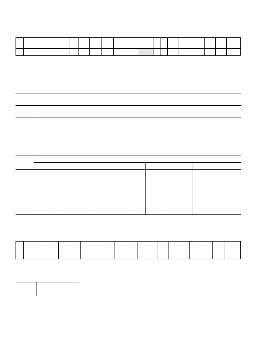
Mono Volume Register (Index 06h)
Reg
No.
Name
D15
D14
D13
D12
D11
D10
D9
D8
D7
D6
D5
*
D4
D3
D2
D1
D0
Default
06h
Mono Volume
MVM
X
X
X
X
X
X
X
X
X
MV5
MV4
MV3
MV2
MV1
MV0
8000h
*Refer to Table II for examples. This register controls the Mono output volume and mute bit. The volume register contains five bits, generating 32 volume levels with
31 steps of 1.5 dB each. Because AC '97 defines 6-bit volume registers, to maintain compatibility, whenever the D5 bit is set to 1, their respective lower five volume
bits are automatically set to 1 by the codec logic. On readback, all lower five bits will read 1s whenever this bit is set to 1. All registers not shown and bits containing
an X are assumed to be reserved.
MV[5:0]
Mono Volume Control. The least significant bit represents 1.5 dB. This register controls the output from 0 dB to a
maximum attenuation of 46.5 dB.
MVM
Mono Volume Mute. When this bit is set to 1, the channel is muted.
Table II. Volume Settings for Mono
Control Bits D[4:0] for Mono (06h)
D15
WRITE
READBACK
Function
0
0 0000
0 0000
0 dB Gain
0
0 1111
0 1111
≠22.5 dB Gain
0
1 1111
1 1111
≠46.5 dB Gain
1
x xxxx
x xxxx
≠
dB Gain, Muted
x in the above table is a wild card and has no effect on the value.
Headphones Volume Register (Index 04h)
Reg
No.
Name
D15
D14 D13 D12
D11
D10 D9 D8
D7
D6 D5
D4
D3
D2
D1 D0 Default
04h
Headphones
HPM
X LHV5 LHV4 LHV3 LHV2 LHV1 LHV0 HPRM
* X RHV5 RHV4 RHV3 RHV2
RHV1 RHV0 8000h
Volume
*For AC '97 compatibility, Bit D7 is available only by setting the MSPLT bit, Register 76h. The MSPLT bit enables separate mute bits for the left and right
channels. If MSPLT is not set, Bit D7 has no effect.
REV. 0
≠12≠
AD1888
Phone_in Volume Register (Index 0Ch)
Reg
No. Name
D15
D14
D13
D12
D11
D10
D9
D8
D7
D6
D5
D4
D3
D2
D1
D0
Default
0Ch Phone_in Volume PHM X
X
X
X
X
X
X
X
X
X
PHV4
PHV3
PHV2
PHV1
PHV0
8008h
All registers not shown and bits containing an X are assumed to be reserved. Refer to Table III for examples.
PHV[4:0]
Phone Volume. Allows setting the Phone Volume attenuator in 32 volume levels with 31 steps of 1.5 dB each. The
LSB represents 1.5 dB, and the gain range is +12 dB to ≠34.5 dB. The default value is 0 dB, with the mute bit enabled.
PHM
Phone Mute. When this bit is set to 1, the Phone channel is muted.
MIC Volume Register (Index 0Eh)
Reg
No. Name
D15
D14
D13
D12
D11
D10
D9
D8
D7
D6
D5
D4
D3
D2
D1
D0
Default
0Eh MIC Volume
MCM
X
X
X
X
X
X
X
X
M20
X
MCV4
MCV3
MCV2
MCV1 MCV0 8008h
All registers not shown and bits containing an X are assumed to be reserved. Refer to Table III for examples.
MCV[4:0]
MIC Volume Gain. Allows setting the MIC Volume attenuator in 32 volume levels. The LSB represents 1.5 dB,
and the gain range is +12 dB to ≠34.5 dB. The default value is 0 dB, with mute enabled.
M20
MIC Gain Boost. This bit allows setting additional MIC gain to increase the microphone sensitivity. The nominal
gain boost by default is 20 dB; however, Bits D0 and D1 (MBG[1:0]) on the miscellaneous control bits register
(76h) allow changing the gain boost to 10 dB or 30 dB, if necessary.
0 = Disabled; Gain = 0 dB
1 = Enabled; Default Gain = 20 dB (see Register 76h, Bits D0, D1)
MCM
MIC Mute. When this bit is set to 1, the channel is muted.
Table III. Volume Settings for Phone and MIC
Control Bits D[4:0]
Phone (0Ch) and MIC (0Eh)
D15
WRITE
READBACK
Function
0
0 0000
0 0000
12 dB Gain
0
0 1000
0 1000
0 dB Gain
0
1 1111
1 1111
≠34.5 dB Gain
1
x xxxx
x xxxx
≠ dB Gain, Muted
x in the above table is a wild card, and has no effect on the value.

REV. 0
AD1888
≠13≠
CD Volume Register (Index 12h)
Reg
No. Name
D15
D14
D13
D12
D11
D10
D9
D8
D7
D6
D5
D4
D3
D2
D1
D0
Default
12h CD Volume
CVM
X
X
LCV4 LCV3
LCV2 LCV1 LCV0 CDRM
* X
X
RCV4 RCV3
RCV2
RCV1
RCV0
8808h
*For AC '97 compatibility, Bit D7 is available only by setting the MSPLT bit, Register 76h. The MSPLT bit enables separate mute bits for the left and right channels.
If MSPLT is not set, the Bit D7 has no effect. All registers not shown and bits containing an X are assumed to be reserved. Refer to Table IV for examples.
Line-In Volume Register (Index 10h)
Reg
No. Name
D15
D14
D13
D12
D11
D10
D9
D8
D7
D6
D5
D4
D3
D2
D1
D0
Default
10h Line-In Volume LVM
X
X
LLV4 LLV3
LLV2
LLV1 LLV0
LVRM
* X
X
RLV4 RLV3
RLV2
RLV1 RLV0 8808h
*For AC '97 compatibility, Bit D7 is available only by setting the MSPLT bit, Register 76h. The MSPLT bit enables separate mute bits for the left and right channels.
If MSPLT is not set, the Bit D7 has no effect. All registers not shown and bits containing an X are assumed to be reserved. Refer to Table IV for examples.
RLV[4:0]
Right Line-In Volume. Allows setting the Line-In Right channel attenuator in 32 volume levels with 31 steps of
1.5 dB each. The LSB represents 1.5 dB, and the range is +12 dB to ≠34.d dB. The default value is 0 dB, mute enabled.
LVRM
Right Channel Mute. Once enabled by the MSPLT bit in Register 76h, this bit mutes the right channel separately
from the LIM bit. Otherwise, this bit will always read 0 and will have no effect when set to 1.
LLV[4:0]
Left Line-In Volume. Allows setting the Line-In left channel attenuator in 32 volume levels with 31 steps of 1.5 dB each.
The LSB represents 1.5 dB, and the range is +12 dB to ≠34.5 dB. The default value is 0 dB, mute enabled.
LVM
Line-In Mute. When this bit is set to 1, both the left and the right channels are muted, unless the MSPLT bit in
Register 76h is set to 1, in which case this mute bit will only affect the left channel.
RCV[4:0]
Right CD Volume. Allows setting the CD right channel attenuator in 32 volume levels with 31 steps of 1.5 dB each.
The LSB represents 1.5 dB, and the range is +12 dB to ≠34.5 dB. The default value is 0 dB, mute enabled.
CDRM
Right Channel Mute. Once enabled by the MSPLT bit in Register 76h, this bit mutes the Right channel separately
from the CVM bit. Otherwise this bit will always read 0 and will have no effect when set to 1.
LCV[4:0]
Left CD Volume. Allows setting the CD left channel attenuator in 32 volume levels with 31 steps of 1.5 dB each.
The LSB represents 1.5 dB, and the range is +12 dB to ≠24.5 dB. The default value is 0 dB, mute enabled.
CVM
CD Volume Mute. When this bit is set to 1, both the left and the right channels are muted, unless the MSPLT bit
in Register 76h is set to 1, in which case this mute bit will affect only the left channel.
RAV[4:0]
Right AUX Volume. Allows setting the AUX right channel attenuator in 32 volume levels with 31 steps of 1.5 dB
each. The LSB represents 1.5 dB, and the range is +12 dB to ≠34.5 dB. The default value is 0 dB, mute enabled.
AVRM
Right Channel Mute. Once enabled by the MSPLT bit in Register 76h, this bit mutes the right channel separately
from the AVM bit. Otherwise, this bit will always read 0 and will have no affect when set to 1.
LAV[4:0]
Left PCM Out Volume. Allows setting the PCM left channel attenuator in 32 volume levels. The LSB represents
1.5 dB, and the range is +12 dB to ≠34.5 dB. The default value is 0 dB, mute enabled.
AVM
PCM Out Volume Mute. When this bit is set to 1, both the left and the right channels are muted, unless the
MSPLT bit in Register 76h is set to 1, in which case this mute bit will affect only the left channel.
AUX Volume Register (Index 16h)
Reg
No. Name
D15
D14 D13 D12
D11
D10
D9
D8
D7
D6
D5
D4
D3
D2
D1
D0
Default
16h AUX Volume
AVM
X
X
LAV4 LAV3
LAV2
LAV1
LAV0
AVRM
* X
X
RAV4 RAV3 RAV2 RAV1 RAV0 8808h
*For AC '97 compatibility, Bit D7 is only available by setting the MSPLT bit, Register 76h. The MSPLT bit enables separate mute bits for the left and right channels.
If MSPLT is not set, Bit D7 has no effect. All registers not shown and bits containing an X are assumed to be reserved. Refer to Table IV for examples.
REV. 0
≠14≠
AD1888
ROV[4:0]
Right PCM Out Volume. Allows setting the PCM right channel attenuator in 32 volume levels. The LSB represents
1.5 dB, and the gain range is +12 dB to ≠34.5 dB. The default value is 0 dB, mute enabled.
OMRM
Right Channel Mute. Once enabled by the MSPLT bit in Register 76h, this bit mutes the right channel separately
from the AVM bit. Otherwise, this bit will always read 0 and will have no affect when set to 1.
LOV[4:0]
Left PCM Out Volume. Allows setting the PCM left channel attenuator in 32 volume levels. The LSB represents
1.5 dB, and the range is +12 dB to ≠34.5 dB. The default value is 0 dB, mute enabled.
OM
PCM Out Volume Mute. When this bit is set to 1, both the left and the right channels are muted, unless the
MSPLT bit in Register 76h is set to 1, in which case this mute bit will affect only the left channel.
PCM-Out Volume Register (Index 18h)
Reg
No. Name
D15 D14 D13 D12
D11
D10
D9
D8
D7
D6
D5 D4
D3
D2
D1
D0
Default
18h PCM Out Volume OM X
X
LOV4 LOV3
LOV2
LOV1
LOV0
OMRM
* X
X
ROV4
ROV3
ROV2 ROV1 ROV0 8808h
*For AC '97 compatibility, Bit D7 is available only by setting the MSPLT bit, Register 76h. The MSPLT bit enables separate mute bits for the left and right channels.
If MSPLT is not set, Bit D7 has no effect. All registers not shown and bits containing an X are assumed to be reserved. Refer to Table IV for examples.
Note that depending on the state of the AC97NC bit in Register 76h, this register has the following additional functionality:
For AC97NC = 0, the register also controls the Surround, Center, and LFE DAC Gain/Attenuators.
For AC97NC = 1, the register controls the PCM Out Volume only.
Table IV. Volume Settings for Line-In, CD Volume, AUX, and PCM-Out
Control Bits
Reg. 76h
Line-In (10h), CD (12h), AUX (16h) and PCM-Out (18h)
Left Channel Volume D[12:8]
Right Channel Volume D[4:0]
MSPLT
*
D15 WRITE
READBACK Function
D7
* WRITE
READBACK
Function
0
0
0 0000
0 0000
12 dB Gain
x
0 0000
0 0000
12 dB Gain
0
0
0 1000
0 1000
0 dB Gain
x
0 1000
0 1000
0 dB Gain
0
0
1 1111
1 1111
≠34.5 dB Gain
x
1 1111
1 1111
≠34.5 dB Gain
0
1
x xxxx
x xxxx
≠ dB Gain, Muted
x
x xxxx
x xxxx
≠ dB Gain, Muted
1
0
1 1111
1 1111
≠34.5 dB Gain
1
x xxxx
x xxxx
≠ dB Gain,
Right Only Muted
1
1
x xxxx
x xxxx
≠ dB Gain,
0
1 1111
1 1111
≠34.5 dB Gain
Left Only Muted
1
1
x xxxx
x xxxx
≠ dB Gain, Left Muted 1
x xxxx
x xxxx
≠ dB Gain, Right Muted
*For AC '97 compatibility, Bit D7 is only available by setting the MSPLT bit, Register 76h. The MSPLT bit enables separate mute bits for the left and right channels.
If MSPLT is not set, RM Bit has no effect.
x in the above table is "don't care."
Record Select Control Register (Index 1Ah)
Reg
No. Name
D15
D14
D13
D12
D11
D10
D9
D8
D7
D6
D5
D4
D3
D2
D1
D0
Default
1Ah Record Select
X
X
X
X
X
LS2
LS1
LS0
X
X
X
X
X
RS2
RS1
RS0
0000h
All registers not shown and bits containing an X are assumed to be reserved.
Refer to Table V for examples. Used to select the record source independently for the right and left channels. For MIC recording, see MS bit (Register 20h) for MIC1
and MIC2 input selection.
RS [2:0]
Right Record Select
LS [2:0]
Left Record Select
REV. 0
AD1888
≠15≠
Table V. Settings for Record Select Control
LS [10:8]
Left Record Source
RS [2:0]
Right Record Source
000
MIC
000
MIC
001
CD_L
001
CD_R
010
Muted
010
Muted
011
AUX_L
011
AUX_R
100
LINE_IN_L
100
LINE_IN_R
101
Stereo Mix (L)
101
Stereo Mix (R)
110
Mono Mix
110
Mono Mix
111
PHONE_IN
111
PHONE_IN
RIM[3:0]
Right Input Mixer Gain Control. Each LSB represents 1.5 dB, 0000 = 0 dB, and the gain range is 0 dB to 22.5 dB.
IMRM
Right Channel Mute. Once enabled by the MSPLT bit in Register 76h, this bit mutes the right channel separately
from the IM bit. Otherwise, this bit will always read 0 and will have no effect when set to 1.
LIM[3:0]
Left Input Mixer Gain Control. Each LSB represents 1.5 dB, 0000 = 0 dB, and the gain range is 0 dB to 22.5 dB.
IM
Input Mute. When this bit is set to 1, both the left and the right channels are muted, unless the MSPLT bit in Reg-
ister 76h is set to 1, in which case this mute bit will affect only the left channel.
Table VI. Settings for Record Gain Register
Control Bits
Reg. 76h
Record Gain (1Ch)
Left Channel Input Mixer D[11:8]
Right Channel Input Mixer D[3:0]
MSPLT
*
D15 WRITE
READBACK
Function
D7
*
WRITE
READBACK
Function
0
0
1111
1111
22.5 dB Gain
x
1111
1111
22.5 dB Gain
0
0
0000
0000
0 dB Gain
x
0000
0000
0 dB Gain
0
1
xxxx
xxxx
≠ dB Gain, Muted
x
xxxx
xxxx
≠ dB Gain, Muted
1
0
1111
1111
22.5 dB Gain
1
xxxx
xxxx
≠ dB Gain,
Right Only Muted
1
1
xxxx
xxxx
≠ dB Gain,
0
1111
1111
22.5 dB Gain
Left Only Muted
1
1
xxxx
xxxx
≠ dB Gain,
1
xxxx
xxxx
≠ dB Gain, Right Muted
Left Muted
*For AC '97 compatibility, Bit D7 (RM) is available only by setting the MSPLT bit, Register 76h. The MSPLT bit enables separate mute bits for the left and right
channels. If MSPLT is not set, Bit D7 has no effect.
x is "don't care."
Record Gain Register (Index 1Ch)
Reg
No. Name
D15
D14
D13
D12
D11
D10
D9
D8
D7
D6
D5
D4
D3
D2
D1
D0
Default
1Ch Record Gain
IM
X
X
X
LIM3
LIM2
LIM1
LIM0 IMRM
* X
X
X
RIM3
RIM2 RIM1 RIM0 8000h
*For AC '97 compatibility, Bit D7 is available only by setting the MSPLT bit, Register 76h. The MSPLT bit enables separate mute bits for the left and right channels.
If MSPLT is not set, Bit D7 has no effect. All registers not shown and bits containing an X are assumed to be reserved. Refer to Table VI for examples.

REV. 0
≠16≠
AD1888
General-Purpose Register (Index 20h)
Reg
No.
Name
D15
D14
D13
D12 D11
D10
D9
D8
D7
D6
D5
D4
D3
D2
D1
D0
Default
20h
General-Purpose X
X
X
X
DRSS1 DRSS0
X
MS
LPBK
X
X
X
X
X
X
X
0000h
This register should be read before writing to generate a mask only for the bit(s) that need to be changed. All registers not shown and bits containing an X are
assumed to be reserved.
LPBK
Loopback Control. This bit enables the digital internal loopback from the ADC to the front DAC. This feature is
normally used for test and troubleshooting.
0 = No Loopback (Default)
1 = Loopback PCM digital data from ADC output to DAC
See LBKS bit in Register 0x74 for changing the loopback path to use the Surround or Center/LFE DACs.
MS
MIC Select. Selects Mono MIC input.
0 = Select MIC1, from rear panel MIC jack
1 = Select MIC2, from front panel MIC jack
DRSS [1:0]
Double Rate Slot Select. The DRSS bits specify the slots for the n + 1 sample outputs. PCM L (n + 1) and PCM R
(n + 1) data are by default provided in output slots 10 and 11.
00: PCM L, R n + 1 Data is on Slots 10, 11 (reset default)
01: PCM L, R n + 1 Data is on Slots 7, 8
10: Reserved
11: Reserved
PG[3:0]
Page Selector (Read Only). This register is used to describe page selector capability for extended features.
Reading these bits returns 0h, which describes page selection as vendor specific only.
I0
INTERRUPT ENABLE (R/W). This enables interrupt generation.
0 = Interrupt Generation is Masked (Default)
1 = Interrupt Generation is Unmasked
The S/W should not unmask the interrupt unless ensured by the AC '97 controller that no conflict is possible with
modem slot 12 GPI functionality.
AC '97 2.2 compliant controllers will not likely support audio codec interrupt infrastructure. In that case, S/W could
poll the interrupt status after initiating a sense cycle and waiting for Sense Cycle Max Delay to determine if an inter-
rupting event has occurred.
I4
INTERRUPT STATUS (R/W). This bit provides interrupt status and clear capability.
0 = Interrupt is Clear
1 = Interrupt was Generated
Interrupt event is cleared by writing a 1 to this bit. The interrupt bit will change regardless of condition of interrupt
enable (I0) status. An interrupt in the GPI in slot 12 in the ac link will follow this bit change when interrupt enable
(I0) is unmasked.
Audio Interrupt and Paging Mechanism Register (Index 24h)
Reg
No. Name
D15
D14
D13 D12
D11
D10
D9
D8
D7
D6
D5
D4
D3
D2
D1
D0
Default
24h Audio Interrupt
I4
X
X
X
I0
X
X
X
X
X
X
X
PG3
PG2
PG1
PG0
xxxxh
and Paging
This register controls the audio interrupt and paging mechanism. All registers not shown and bits containing an X are assumed to be reserved.

REV. 0
AD1888
≠17≠
Power-Down Control/Status Register (Index 26h)
Reg
No. Name
D15
D14
D13 D12
D11
D10
D9
D8
D7
D6
D5
D4
D3
D2
D1
D0
Default
26h Power-Down
EAPD
PR6
PR5 PR4
PR3
PR2
PR1
PR0
X
X
X
X
REF
ANL
DAC ADC NA
Control/Status
The ready bits are read only; writing to REF, ANL, DAC, ADC will have no effect. These bits indicate the status for the AD1888 subsections. If the bit is a 1, then
that subsection is ready. Ready is defined as the subsection able to perform in its nominal state. All registers not shown and bits containing an X are assumed to be reserved.
ADC
ADC Sections Ready to Transmit Data
DAC
DAC Sections Ready to Transmit Data
ANL
Analog Amplifiers, Attenuators, and Mixers Ready
REF
Voltage References, V
REF
and V
REFOUT
, up to Nominal Level
PR[6:0]
Codec Power-Down Modes. The first three bits are to be used individually rather than in combination with each
other. PR3 can be used in combination with PR2 or by itself. The mixer and reference cannot be powered down via
PR3 unless the ADCs and DACs are also powered down. Nothing else can be powered up until the reference is up.
PR5 has no effect unless all ADCs, DACs, and the ac-link are powered down. The reference and the mixer can be
either up or down, but all power-up sequences must be allowed to run to completion before PR5 and PR4 are both set.
In multiple codec systems, the master codec's PR5 and PR4 bits control the slave codec. PR5 is also effective in the
slave codec if the master's PR5 bit is clear, but the PR4 bit has no effect except to enable or disable PR5.
EAPD
External Audio Power-Down Control. Controls the state of the EAPD pin.
EAPD = 0 sets the EAPD pin low, enabling an external power amplifier (reset defaults).
EAPD = 1 sets the EAPD pin high, shutting off the external power amplifier.
REV. 0
≠18≠
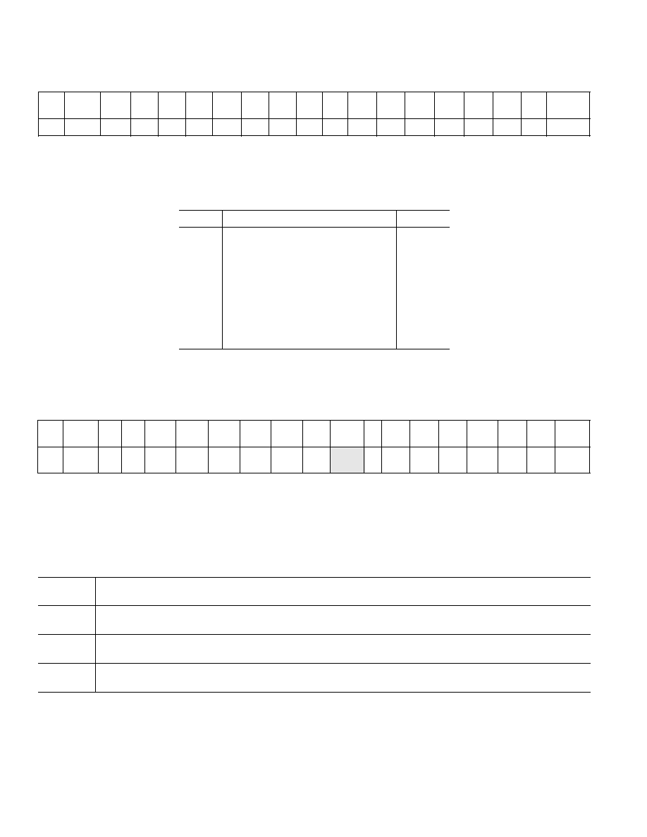
AD1888
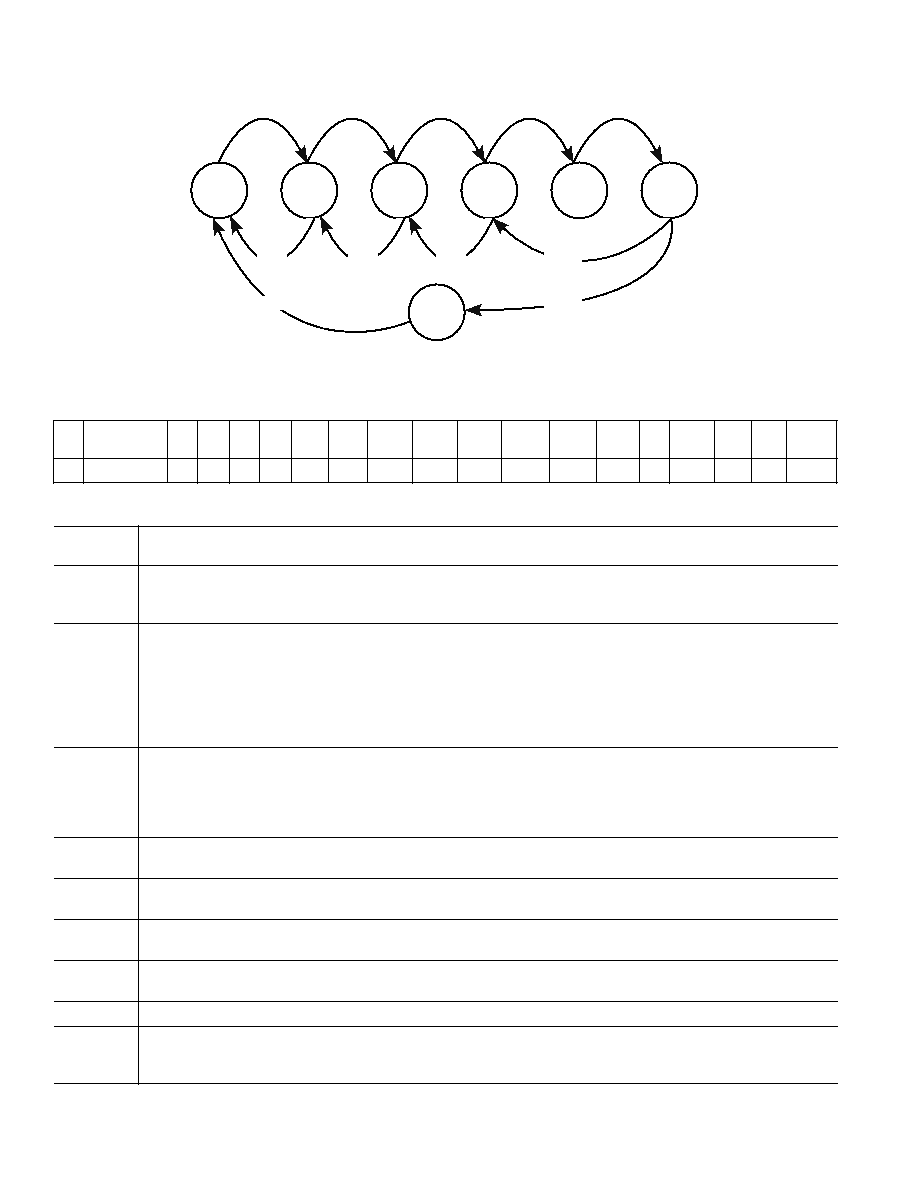
NORMAL
ADCs OFF
PR0
DACs OFF
PR1
ANALOG
OFF
PR2 OR
PR3
DIGITAL I/F
OFF
PR4
SHUT OFF
AC-LINK
PR0 = 1
PR1 = 1
PR2 = 1
PR4 = 1
DEFAULT
PR0 = 0
AND
ADC = 1
PR1 = 0
AND
DAC = 1
PR2 = 0
AND
ANL = 1
WARM
RESET
COLD
RESET
READY = 1
Figure 8. One Example of AC `97 Power-Down/Power-Up Flow
Extended Audio ID Register (Index 28h)
Reg
No. Name
D15 D14 D13 D12 D11
D10
D9
D8
D7
D6
D5
D4
D3
D2
D1
D0
Default
28h Ext'd Audio ID ID1 ID0
X
X
REV1 REV0 AMAP LDAC
SDAC
CDAC
DSA1
DSA0
X
SPDIF DRA VRA x3C7h
The extended audio ID register identifies which extended audio features are supported. A nonzero extended audio ID value indicates one or more of the extended
audio features are supported. All registers not shown and bits containing an X are assumed to be reserved.
VRA
Variable Rate PCM Audio Support (Read Only).
This bit returns a 1 when read to indicate that the Variable Rate PCM Audio is supported.
DRA
Double Rate Audio (Read Only).
This bit returns a 1 when read to indicate that the optional Double Rate RCM Audio is supported for PCM L and
PCM R.
SPDIF
SPDIF Support (Read Only). This bit returns a 1 when read to indicate that the SPDIF transmitter is supported
(IEC958).
This bit is also used to validate that the SPDIF transmitter output is actually enabled. The SPDIF bit is only
allowed to be set high if the SPDIF pin (48) is pulled down at power-up, enabling the codec transmitter logic. If the
SPDIF pin is floating or pulled high at power-up, the transmitter logic is disabled and therefore this bit returns a
low, indicating that the SPDIF transmitter is not available. This bit must always be read back to verify that the
SPDIF transmitter is actually enabled.
DSA[1,0]
DAC Slot Assignments (Read/Write) (Reset Default = 00)
00 DACs 1, 2 = 3 and 4
DACs 3, 4 = 7 and 8
DACs 5, 6 = 6 and 9
01 DACs 1, 2 = 7 and 8
DACs 3, 4 = 6 and 9
DACs 5, 6 = disabled
10 DACs 1, 2 = 6 and 9
DACs 3, 4 = disabled
DACs 5, 6 = disabled
11 Reserved
CDAC
PCM CENTER DAC Support (Read Only).
This bit returns a 1 when read to indicate that PCM center DAC is supported.
SDAC
PCM Surround DAC Support (Read Only).
This bit returns a 1 when read to indicate that PCM surround left and right DACs are supported.
LDAC
PCM LFE DAC Support (Read Only),
This bit returns a 1 when read to indicate that PCM LFE DAC is supported.
AMAP
Slot DAC Mappings Based on Codec ID (Read Only).
This bit returns a 1 when read to indicate that slot/DAC mappings based on codec ID are supported.
REV[1,0]
REV[1,0] = 01 indicates codec is AC '97 revision 2.2 compliant (Read Only).
ID[1:0]
Indicates Codec Configuration (Read Only).
00 = Primary
01, 10, 11 = Secondary

REV. 0
AD1888
≠19≠
Extended Audio Status and Control Register (Index 2Ah)
Reg
No. Name
D15
D14 D13 D12 D11 D10
D9 D8
D7
D6
D5
D4
D3
D2
D1
D0
Default
2Ah Extended Audio VFORCE X
PRK PRJ
PRI SPCV X
ELDAC ESDAC ECDAC SPSA1 SPSA0 X
ESPDIF EDRA EVRA 0xx0h
Stat/Ctrl
The extended audio status and control register is a read/write register that provides status and control of the extended audio features. All registers not shown and bits
containing an X are assumed to be reserved.
EVRA
Variable Rate Audio (Read/Write).
EVRA = 0, sets fixed sample rate audio at 48 kHz (Reset Default).
EVRA = 1, enables variable rate audio mode (enables sample rate registers and SLOTREQ signaling).
EDRA
Double Rate Audio.
EDRA = 1 enables double rate audio mode in which data from PCM L and PCM R in output slots 3 and 4 is used
in conjunction with PCM L (n + 1) and PCM R (n + 1) data to provide DAC streams at twice the sample rate
designated by the PCM front sample rate control register. When using the double rate audio, only the front DACs
are supported and all other DACs (surround, center, and LFE) are automatically powered down.
Note that EDRA can be used without VRA; in that case, the converter rates are forced to 96 kHz if EDRA = 1.
ESPDIF
SPDIF Transmitter Subsystem Enable/Disable Bit (Read/Write).
ESPDIF = 1 enables the SPDIF transmitter.
ESPDIF = 0 disables the SPDIF transmitter (default).
SPSA[1,0]
SPDIF Slot Assignment Bits (Read/Write).
These bits control the SPDIF slot assignment and respective defaults, depending on the codec ID configuration.
See the following table.
ECDAC
Center DAC Status (Read Only).
ECDAC = 1 indicates the PCM center DAC is ready.
ESDAC
Surround DAC status (Read Only).
ESDAC = 1 indicates the PCM surround DACs are ready.
ELDAC
LFE DAC status (Read Only).
ELDAC = 1 indicates the PCM LFE DAC is ready.
SPCV
SPDIF Configuration Valid (Read Only). Indicates the status of the SPDIF transmitter subsystem, enabling the
driver to determine if the currently programmed SPDIF configuration is supported. SPCV is always valid, indepen-
dent of the SPDIF enable bit status.
SPCV = 0 indicates current SPDIF configuration (SPSA, SPSR, DAC slot rate, DRS) is not valid (not supported).
SPCV = 1 indicates current SPDIF configuration (SPSA, SPSR, DAC slot rate, DRS) is valid (supported).
PRI
Center DAC Power-Down (Read/Write).
PRI = 1 turns off the PCM Center DAC.
PRJ
Surround DACs Power-Down (Read/Write).
PRJ = 1 turns off the PCM surround DACs.
PRK
LFE DAC Power-Down (Read/Write).
PRK = 1 turns off the PCM LFE DAC.
VFORCE
Validity Force Bit (Reset Default = 0).
When asserted, this bit forces the SPDIF stream validity flag (Bit 28 within each SPDIF L/R subframe) to be con-
trolled by the V bit (D15) in Register 3Ah (SPDIF control register).
VFORCE = 0 and V = 0; the Validity Bit is managed by the codec error detection logic.
VFORCE = 0 and V = 1; the Validity Bit is forced high, indicating subframe data is invalid.
VFORCE = 1 and V = 0; the Validity Bit is forced low, indicating subframe data is valid.
VFORCE = 1 and V = 1; the Validity Bit is forced high, indicating subframe data is invalid.
REV. 0
≠20≠
AD1888
AC '97 2.2 AMAP Compliant Default SPDIF Slot Assignments
Codec ID
Function
SPSA = 00
SPSA = 01
SPSA = 10
SPSA = 11
00
2-Ch Primary w/SPDIF
3 and 4
7 and 8 [default]
6 and 9
10 and 11
00
4-Ch Primary w/SPDIF
3 and 4
7 and 8
6 and 9[default]
10 and 11
00
6-Ch Primary w/SPDIF
3 and 4
7 and 8
6 and 9
10 and 11[default]
01
+2-Ch Secondary w/SPDIF
3 and 4
7 and 8
6 and 9[default]
01
+4-Ch Secondary w/SPDIF
3 and 4
7 and 8
6 and 9
10 and 11[default]
10
+2-Ch Secondary w/SPDIF
3 and 4
7 and 8
6 and 9[default]
10
+4-Ch Secondary w/SPDIF
3 and 4
7 and 8
6 and 9
10 and 11[default]
11
+2-Ch Secondary w/SPDIF
3 and 4
7 and 8
6 and 9
10 and 11[default]
PCM Front DAC Rate Register
(Index 2Ch)
Reg
No. Name
D15
D14
D13
D12
D11
D10
D9
D8
D7
D6
D5
D4
D3
D2
D1
D0
Default
2Ch PCM Front
SRF15 SRF14 SRF13 SRF12 SRF11 SRF10 SRF9 SRF8 SRF7 SRF6 SRF5 SRF4 SRF3 SRF2 SRF1 SRF0 BB80h
DAC Rate
This read/write Sample Rate Control Register contains 16-bit unsigned value, representing the rate of operation in Hz.
SRF[15:0]
Sample Rate.
The sampling frequency range is from 7 kHz (1B58h) to 48 kHz (BB80h) in 1 Hz increments. If zero is written to
EVRA, the sample rate is reset to 48 kHz.
PCM LFE (and CENTER) DAC Rate Register (Index 30h)
Reg
No. Name
D15
D14
D13
D12
D11
D10
D9
D8
D7
D6
D5
D4
D3
D2
D1
D0
Default
30h PCM LFE/
SRCL15 SRCL14 SRCL13 SRCL12 SRCL11 SRCL10 SRCL9 SRCL8 SRCL7 SRCL6 SRCL5 SRCL4 SRCL3 SRCL2 SRCL1 SRCL0 BB80h
C DAC
Rate
This read/write sample rate control register contains 16-bit unsigned value, representing the rate of operation in Hz.
This register sets the sample rate for the LFE DAC and Center DAC. This register's reset default is to be locked to the PCM Front DAC sample rate register (2-Ch) .
To unlock the register bit, SRU in Register 76h must be asserted.
SRCL[15:0]
Sample Rate.
The sampling frequency range is from 7 kHz (1B58h) to 48 kHz (BB80h) in 1 Hz increments.
If zero is written to EVRA, the sample rate is reset to 48 kHz.
PCM Surround DAC Rate Register (Index 2Eh)
Reg
No. Name
D15
D14
D13
D12
D11
D10
D9
D8
D7
D6
D5
D4
D3
D2
D1
D0
Default
2Eh PCM Surr
SRS15 SRS14 SRS13 SRS12 SRS11 SRS10 SRS9 SRS8 SRS7 SRS6
SRS5
SRS4 SRS3
SRS2 SRS1 SRS0
BB80h
DAC Rate
This read/write Sample Rate Control Register contains 16-bit unsigned value, representing the rate of operation in Hz.
This register sets the sample rate for the surround DAC. This register's reset default is to be locked to the PCM front DAC sample rate register (2-Ch).
To unlock this register, Bit SRU in Register 76h must be asserted.
SRS[15:0]
Sample Rate.
The sampling frequency range is from 7 kHz (1B58h) to 48 kHz (BB80h) in 1 Hz increments.
If zero is written to the EVRA bit, the sample rate is reset to 48 kHz.
PCM ADC Rate Register (Index 32h)
Reg
No. Name
D15
D14
D13
D12
D11
D10
D9
D8
D7
D6
D5
D4
D3
D2
D1
D0
Default
32h
PCM L/R
SRA15
SRA14 SRA13 SRA12 SRA11 SRA10 SRA9 SRA8 SRA7 SRA6 SRA5 SRA4 SRA3 SRA2 SRA1 SRA0 BB80h
ADC Rate
This read/write sample rate control register contains 16-bit unsigned value, representing the rate of operation in Hz.
SRA[15:0]
Sample Rate.
The sampling frequency range is from 7 kHz (1B58h) to 48 kHz (BB80h) in 1 Hz increments.
If zero is written to EVRA, the sample rate is reset to 48 kHz.
REV. 0
AD1888
≠21≠
CNT[5:0]
Center Volume Control
CM
Center Volume Mute. When this bit is set to 1, the channel is muted.
LFE[5:0]
LFE Volume Control
LM
LFE Volume Mute. When this bit is set to 1, the channel is muted.
CENTER/LFE Volume Control Register (Index 36h)
Reg
No. Name
D15 D14
D13
*
D12
D11
D10
D9
D8
D7
D6
D5
*
D4
D3
D2
D1
D0
Default
36h Center/LFE
LM
X
LFE5
LFE4
LFE3
LFE2
LFE1
LFE0
CM
X
CNT5 CNT4 CNT3 CNT2
CNT1 CNT0 8080h
Volume
All registers not shown and bits containing an X are assumed to be reserved.
Refer to Table VII for examples. This register controls the LFE output volume and mute bit. The volume registers contain five bits, generating
32 volume levels with 31 steps of 1.5 dB each. If MSPLT is not set, Bit D7 has no effect.
*Because AC '97 defines 6-bit volume registers, to maintain compatibility, whenever the D5 or D13 bit is set to 1, its respective lower five volume bits are automati-
cally set to 1 by the codec logic. On readback, all lower five bits will read 1s whenever this bit is set to 1.
Note that depending on the state of the AC97NC bit in Register 76h, this register operates as follows:
For AC97NC = 0, the register controls the center and LFE output pin attenuators. Range is 0 dB to ≠46.5 dB.
For AC97NC = 1, the register controls the center and LFE DAC gain/attenuators. Range is +12 dB to ≠34.5 dB.
Table VII. Settings for Center/LFE Register
Control Bits
CENTER and LFE Volume (36h)
CENTER D[5:0] and LFE D[13:8]
D15/D7
WRITE
READBACK
Function with AC97NC = 0
Function with AC97NC = 1
0
00 0000
00 0000
0 dB Gain
12 dB Gain
0
00 1111
00 1111
≠22 dB Gain
≠10.5 dB Gain
0
01 1111
01 1111
≠46.5 dB Gain
≠34.5 dB Gain
0
1x xxxx
01 1111
≠46.5 dB Gain
Not Applicable
1
xx xxxx
xx xxxx
Muted
Muted
Surround Volume Control Register (Index 38h)
Reg
No.
Name
D15
D14 D13
* D12
D11
D10
D9
D8
D7
D6
D5
*
D4
D3
D2
D1
D0
Default
38h
Surround
MUTE_L X
LSR5 LSR4 LSR3 LSR2
LSR1 LSR0
MUTE_R X
RSR5 RSR4 RSR3 RSR2
RSR1
RSR0 8080h
Volume
*Refer to Table VIII for examples. This register controls the surround volume controls for both stereo channels and mute bits. Each volume subregister contains
five bits, generating 32 volume levels with 31 steps of 1.5 dB each. Because AC '97 defines 6-bit volume registers, to maintain compatibility, whenever the D5 or
D13 Bit is set to 1, its respective lower five volume bits are automatically set to 1 by the coded logic. On readback , all lower five bits will read 1s whenever these
bits are set to 1.
Note that depending on the state of the AC97NC bit in Register 76h, this register operates as follows:
For AC97NC = 0, the register controls the surround output pin attenuators. Range is 0 dB to ≠46.5 dB.
For AC97NC = 1, the register controls the surround DAC gain/attenuators. Range is +12 dB to ≠34.5 dB.
RSR[5:0]
Right Surround Volume Control
MUTE_R
Right Surround Volume Mute. When this bit is set to 1, the right channel is muted.
LSR[5:0]
Left Surround Volume Control
MUTE_L
Left Surround Volume Mute. When this bit is set to 1, the left channel is muted.
REV. 0
≠22≠
AD1888
SPDIF Control Register (Index 3Ah)
Reg
No. Name
D15
D14
D13
D12
D11
D10
D9
D8
D7
D6
D5
D4
D3
D2
D1
D0
Default
3Ah SPDIF
V
X
SPSR1
SPSR0
L
CC6
CC5 CC4
CC3
CC2
CC1
CC0
PRE
COPY
/AUD PRO
2000h
Control
All registers not shown and bits containing an X are assumed to be reserved.
Register 3Ah is a read/write register that controls SPDIF functionality and manages bit fields propagated as channel status (or subframe in the V case). With the
exception of V, this register should only be written to when the SPDIF transmitter is disabled (SPDIF Bit in Register 2Ah is 0). This ensures that control and status
information starts up correctly at the beginning of SPDIF transmission.
PRO
Professional. 1 indicates professional use of channel status, 0 indicates consumer.
/AUD
Non-Audio. 1 indicates data is non PCM format, 0 indicates data is PCM.
COPY
Copyright. 1 indicates copyright is asserted, 1 indicates copyright is not asserted.
PRE
Pre-emphasis. 1 indicates filter pre-emphasis is 50
µs/15 µs, 0 indicates pre-emphasis is none.
CC[6-0]
Category Code. Programmed according to IEC standards, or as appropriate.
L
Generation Level. Programmed according to IEC standards, or as appropriate.
SPSR[1,0]
SPDIF Transmit Sample Rate:
SPSR[1:0] = 00 Transmit Sample Rate = 44.1 kHz
SPSR[1:0] = 01 Reserved
SPSR[1:0] = 10 Transmit Sample Rate = 48 kHz (default)
SPSR[1:0] = 11 Not supported.
V
Validity. This bit affects the Validity flag (Bit 28 transmitted in each SPDIF L/R subframe) and enables the SPDIF
transmitter to maintain connection during error or mute conditions.
V = 1 Each SPDIF subframe (L + R) has Bit 28 set to 1. This tags both samples as invalid.
V = 0 Each SPDIF subframe (L + R) has Bit 28 set to 0 for valid data and 1 for invalid data (error condition).
Note that when V = 0, asserting the VFORCE bit (D15) in Register 2Ah (Ext'd Audio Stat/Ctrl) will force the
Validity flag low, marking both samples as valid.
Table VIII. Settings for Surround Register
Control Bits
Surround Volume (38h)
Left Surround D[13:8]
Right Surround D[5:0]
D15/D7
WRITE
READBACK
Function with AC97NC = 0
Function with AC97NC = 1
0
00 0000
00 0000
0 dB Gain
12 dB Gain
0
00 1111
00 1111
≠22 dB Gain
≠10.5 dB Gain
0
01 1111
01 1111
≠46.5 dB Gain
≠34.5 dB Gain
0
1x xxxx
01 1111
≠46.5 dB Gain
Not Applicable
1
xx xxxx
xx xxxx
Muted
Muted

REV. 0
AD1888
≠23≠
JS0INT
Indicates Pin JS0 has generated an interrupt. Remains set until the software services JS0 interrupt, i.e., JS0 ISR
should clear this bit by writing a 0 to it. Note that the interrupt to the system is actually an OR combination of this
bit and JS1INT. Also, note that the actual interrupt implementation is selected by the INTS bit (Register 76h).
It is also possible to generate a software system interrupt by writing a 1 to this bit.
JS1INT
Indicates Pin JS1 has generated an interrupt. Remains set until the software services JS1 interrupt, i.e., JS1 ISR
should clear this bit by writing a 0 to it. See the JS0INT description for additional details.
JS0ST
JS0 STATE. This bit always reports the logic state of the JS0 pin.
JS1ST
JS1 STATE. This bit always reports the logic state of the JS1 pin.
JS0MD
JS0 Mode. This bit selects the operation mode for the JS0 pin.
0 = Jack Sense Mode (reset default)
1 = Interrupt Mode
JS1MD
JS1 Mode. This bit selects the operation mode for the JS1 pin.
0 = Jack Sense Mode (reset default)
1 = Interrupt Mode
JS0TMR
JS0 Timer Enable. If this bit is set to a 1, JS0 must be high for greater than 278 ms to be recognized.
JS1TMR
JS1 Timer Enable. If this bit is set to a 1, JS1 must be high for greater than 278 ms to be recognized.
JSMT[2,0]
JS Mute Enable Selector. These three bits select and enable the Jack Sense muting action (see Table IX).
JS0DMX
JS0 Down Mix Control Enable. This bit enables JS0 to control the down-mix function. This function allows a
digital mix of six channels of audio into 2-channel audio. The mix can then be routed to the stereo Line_OUT or
HP_OUT jacks. When this bit is set to 1, JS0 = 1 will activate the down-mix conversion.
See the DMIX description in Register 76h. The DMIX bits select the down-mix implementation type and can also
force the function to be activated.
JS1DMX
JS1 Down Mix Control Enable. This bit enables 2-channel to 6-channel audio spread function when both Jack
Senses are active (logic state 1).
Note that the SPRD bit can also force the spread function without being gated by the Jack Senses. See this bit's
description in Register 76h for a better understanding of the spread function.
JS1SPRD
JS Spread Control Enable. This bit enables 2-channel to 6-channel audio spread function when both Jack Senses are
active (logic state 1).
Note that the SPRD bit can also force the spread function without being gated by the Jack Senses. See this bit's
description in Register 76h for a better understanding of the spread function.
Jack Sense/Audio Interrupt Status Register (Index 72h)
Reg
No. Name
D15
D14
D13
D12
D11
D10
D9
D8
D7
D6
D5
D4
D3
D2
D1
D0
Default
72h
Jack
JS1
JS1
JS0
JS
JS
JS
X
X
JS1
JS0
JS1
JS0
JS1
JS0
JS1
JS0
0000h
Sense
SPRD DMX
DMX
MT2
MT1
MT0
TMR
TMR
MD
MD
ST
ST
INT
INT
All register bits are read/write except for JS0ST and JS1ST, which are read only.

REV. 0
≠24≠
AD1888
Table IX. Jack Sense Mute Select (JSMT [2:0])
HP
LINE
C/LFE
MONO
JS1
JS0
JSMT2
JSMT1
JSMT0
OUT
OUT
OUT
OUT
NOTES
NA
NA
0
0
0
ACTIVE
ACTIVE
ACTIVE
ACTIVE
JS0 and JS1 ignored.
OUT (0)
OUT (0)
0
0
1
ACTIVE
FMUTE
FMUTE
ACTIVE
JS0 no mute action,
OUT (0)
IN (1)
0
0
1
ACTIVE
FMUTE
FMUTE
ACTIVE
JS1 mutes mono and
IN (1)
OUT (0)
0
0
1
ACTIVE
ACTIVE
ACTIVE
ACTIVE
enables LINE_OUT
IN (1)
IN (1)
0
0
1
ACTIVE
ACTIVE
ACTIVE
ACTIVE
and C/LFE.
Standard 6-channel
config.
OUT (0)
OUT (0)
1
0
0
ACTIVE
FMUTE
FMUTE
ACTIVE
JS0 = 0 and JS1 = 0
OUT (0)
IN (1)
1
0
0
ACTIVE
ACTIVE
ACTIVE
FMUTE
enables mono.
IN (1)
OUT (0)
1
0
0
ACTIVE
FMUTE
FMUTE
FMUTE
JS1 = 1 enables front
IN (1)
IN (1)
1
0
0
ACTIVE
FMUTE
FMUTE
FMUTE
only.
JS0 = 1 enables all rear.
6-chan config with
front jack wrapback.
OUT (0)
OUT (0)
1
0
1
FMUTE
FMUTE
FMUTE
ACTIVE
JS0 no mute action,
OUT (0)
IN (1)
1
0
1
FMUTE
FMUTE
FMUTE
FMUTE
JS1 mutes mono and
IN (1)
OUT (0)
1
0
1
ACTIVE
ACTIVE
ACTIVE
FMUTE
enables LINE_OUT
IN (1)
IN (1)
1
0
1
ACTIVE
ACTIVE
ACTIVE
FMUTE
+ HP_OUT + C/LFE.
Standard 6-channel
config.
NA
NA
1
1
0
**
**
**
**
**
Reserved
NA
NA
1
1
1
**
**
**
**
**
Reserved
NA
NA
0
1
1
**
**
**
**
**
Reserved
FMUTE = Output is forced to mute independent of the respective Volume register setting.
ACTIVE = Output is not muted and its status is dependent on the respective Volume register setting.
OUT = Nothing plugged into the jack and therefore the JS status is 0 (via the load resistor pull-down).
IN = Jack has plug inserted and therefore the JS status is 1 (via the codec JS internal pull-up).

REV. 0
AD1888
≠25≠
Serial Configuration Register (Index 74h)
Reg
No. Name D15
D14
D13
D12
D11
D10 D9 D8
D7 D6
D5 D4 D3 D2
D1
D0
Default
74h Serial
SLOT16 REGM2 REGM1 REGM0 REGM3 DRF X
CHEN X LBKS1 LBKS0 INTS X
SPAL SPDZ SPLNK 1001h
Configuration
All registers not shown and bits containing an X are assumed to be reserved.
Note that this register is not reset when Register 00h (Reset Register) is written to (soft reset).
SPLNK
SPDIF Link. This bit enables the SPDIF to link with the front DACs for data requesting.
0 = SPDIF and DAC are not linked.
1 = SPDIF and DAC are linked and receive the same data requests (reset default).
SPDZ
SPDIF DACZ.
0 = Repeat last sample out of the SPDIF stream if FIFO underruns (reset default).
1 = Forces midscale sample out the SPDIF stream if FIFO underruns.
SPAL
SPDIF ADC Loop-Around.
0 = SPDIF transmitter is connected to the AC-Link stream (reset default).
1= SPDIF transmitter is connected to the digital ADC stream, not the AC-Link.
INTS
Interrupt Mode Select. This bit selects the JS interrupt implementation path.
0 = Bit 0 SLOT 12 (modem interrupt) (reset default).
1 = Slot 6 Valid Bit (MIC ADC interrupt).
LBKS[1:0]
Loop-Back Selection. These bits select the internal digital loop-back path when LPBK bit is active (see Register 20h)
00 = Loop-back through the front DACs (reset default).
01 = Loop-back through the surround DACs.
10 = Reserved
11 = Loop-back through the center and LFE DACs (center DAC loops back from the ADC left channel, the LFE
DAC from the ADC right channel).
CHEN
Chain Enable. This bit enables chaining of a slave codec SDATA_IN stream into the ID0 pin (Pin 45).
0 = Disable chaining (reset default).
1 = Enable chaining into ID0 pin.
DRF
DAC Request Force. This allows the AD1888 to synchronize DAC requests with the AD1981A/B.
0 = Normal DAC requesting sequence (reset default).
1 = Synchronize to AD1981A/B DAC requests.
REGM3
Slave 3 Codec Register Mask
REGM0
Master Codec Register Mask
REGM1
Slave 1 Codec Register Mask
REGM2
Slave 2 Codec Register Mask
SLOT16
Enable 16-Bit Slot Mode. SLOT16 makes all ac-link slots 16 bits in length, formatted into 16 slots. This is a
preferred mode for DSP serial port interfacing.

REV. 0
≠26≠
AD1888
MBG[1:0]
MIC Boost Gain Select Register.
These two bits allow changing the MIC preamp gain from the nominal 20 dB gain. Both MIC1/MIC2 and MIC2
preamps will be set to the same selected gain.
Note that this gain takes effect only while Bit D6 (M20) on the MIC volume register (0Eh) is set to 1; otherwise, the
MIC boost block has a gain of 0 dB.
00 = 20 dB gain (reset default)
01 = 10 dB gain
10 = 30 dB gain
11 = reserved
VREFD
V
REFOUT
Disable. Disables V
REFOUT
, placing it into High-Z out mode.
Note that this bit overrides the VREFH bit selection (see below).
0 = V
REFOUT
pin is driven by the internal reference (reset default).
1 = V
REFOUT
pin is placed into High-Z out mode.
VREFH
V
REFOUT
High. Changes V
REFOUT
from 2.25 V to 3.70 V for PC2001 compliant MIC bias applications.
0 = V
REFOUT
pin is set to 2.25 V output (reset default).
1 = V
REFOUT
pin is set to 3.70 V output.
SRU
Sample Rate Unlock. Controls DAC sample rate locking.
0 = All DAC sample rates are locked to the front sample rate (reset default).
1 = DAC sample rates can be set independently for front, surround, and LFE.
LOSEL
LINE_OUT Amplifiers Input Select. This bit allows the LINE_OUT output amplifiers to be driven by the mixer
or the surround DACs. The main purpose for this is to allow swapping of the front and surround channels to make
better use of the SURR/HP_OUT output amplifiers. This bit should normally be used in tandem with the HPSEL
bit (see below).
0 = LINE_OUT amplifiers are driven by the mixer outputs (reset default).
1 = LINE_OUT amplifiers are driven by the surround DAC outputs.
SPRD
SPREAD Enable. This bit enables spreading of 2-channel media to all six output channels. This function is imple-
mented in the analog section by using the output selector controls line for the center/LFE, surround, and Line_out
output channels. Note that the Jack Sense pins can also be set up to control (gate) this function, depending on the
JSSPRD bit (see Register 72h).
0 = No spreading occurs unless activated by the Jack Senses and JSSPRD bits (reset default).
1 = The SPRD selector drives the center and LFE outputs from the MONO_OUT, the HPSEL selector drives the
SURR/HP_OUT outputs from the mixer outputs, and the LOSEL selector drives the LINE_OUT outputs also
from the mixer outputs.
Note that the SPRD bit overrides the current output selector control lines set up by bits LOSEL and HPSEL as
follows: LOSEL = 0 and HPSEL = 1.
Miscellaneous Control Bit Register (Index 76h)
Reg
De-
No. Name D15
D14
D13
D12
D11
D10
D9
D8
D7
D6
D5
D4
D3
D2
D1
D0
fault
76h Misc
DACZ AC97NC MSPLT LODIS CLDIS HPSEL DMIX1 DMIX0 SPRD X
LOSEL SRU VREFH VREFD MBG1 MBG0 0000h
Control
Bits

REV. 0
AD1888
≠27≠
DMIX[1:0]
Down Mix Mode Select. Provides analog down-mixing of the center, LFE, and/or surround channels into the
mixer channels. This allows the full content of 5.1 or quad media to be played through stereo headphones or
speakers.
Note that the Jack Sense pins can also be set up to control (gate) this function depending on the JS0DMX and
JS1DMX Bits (see Register 72h).
The upper bit allows forcing the down-mix function:
DMIX[1] = 0, no down-mix unless activated by the Jack Sense and JSxDMX bits (default).
DMIX[1] = 1, forces down-mix function.
The lower bit selects the down-mix type:
DMIX[0] = 0, selects 6-to-4 down-mix. The center and LFE channels are summed equally into the mixer left and
right channels (default).
DMIX[0] = 1, selects 6-to-2 down-mix. The surround left and right channels are summed into the mixer left and
right channels.
Default for DMIX[1:0] is 00.
HPSEL
Headphone Amplifier Input Select. This bit allows the headphone power amps to be driven from the surround
DACs or from the mixer outputs. There are two reasons for this: one is to allow 2-channel media to use the
higher power headphone amplifiers available on the SURR/HP_OUT outputs; the other is to allow spreading of
2-channel media to the surround outputs.
Together with the LOSEL bit (see above), this bit also provides for analog swapping of the mixer (front) and sur-
round outputs.
0 = SURR_OUT/HP_OUToutputs are driven by the surround DACs (reset default).
1 = SURR_OUT/HP_OUToutputs are driven by the mixer outputs.
CLDIS
Center and LFE Disable. Disables the center and LFE output pins, placing them into High-Z mode so that the
assigned output audio jack(s) can be shared for MIC inputs or other functions.
0 = Center and LFE output pins have normal audio drive capability (reset default).
1 = Center and LFE output pins are placed into High-Z mode.
LODIS
Line_out Disable. Disables the Line_out pins (L/R), placing them into High-Z mode so that the assigned output
audio jack can be shared for Line Input function.
0 = Line_out pins have normal audio drive capability (reset default).
1 = Line_out pins are placed into High-Z mode.
MSPLT
Mute Split. Allows separate mute control bits for master, HP, Line_in, CD, PCM OUT, and record volume/gain
control registers.
0 = Both left and right channel mutes are controlled by Bit D15 in the respective registers (reset default).
1 = Bit D15 affects only the left channel mute and Bit D7 affects only the right channel mute.
AC97NC
AC '97 No Compatibility Mode. This bit allows the surround, center, and LFE volume control registers and
output attenuators to operate in a more functional mode than defined by the AC97 2.2 spec. This is called ADI
compatibility mode.
In AC '97 compatibility mode, the DAC gain/attenuators for the surround, center, and LFE are controlled by
Register 18h (PCM volume). The output pin attenuators for the surround are controlled by Register 38h, and the
output pin attenuators for the center and LFE are controlled by Register 36h.
In ADI compatibility mode, the Surround DAC gain/attenuators are controlled by Register 38h, and the
Center/LFE DACs are controlled by Register 36h.
The output pin attenuators for Center/LFE are controlled by Register 02h (Master Volume), and the output pin
attenuators for Surround are controlled by Register 04h.
0 = AC97 compatibility mode (reset default).
1 = ADI compatibility mode.
DACZ
DAC Zero-Fill. Determines DAC data fill under starved condition.
0 = DAC data is repeated when DACs are starved for data (reset default).
1 = DAC data is zero-filled when DACs are starved for data.
REV. 0
≠28≠
AD1888
Vendor ID Register (Index 7Ch≠7Eh)
Reg
No. Name
D15
D14 D13
D12
D11
D10
D9
D8
D7
D6
D5
D4
D3
D2
D1
D0
Default
7Ch Vendor ID1 F7
F6
F5
F4
F3
F2
F1
F0
S7
S6
S5
S4
S3
S2
S1
S0
4144h
S[7:0] This register is ASCII encoded to A.
F[7:0] This register is ASCII encoded to D.
Reg
No. Name
D15 D14 D13 D12 D11 D10 D9
D8
D7
D6
D5
D4
D3
D2
D1
D0
Default
7Eh Vendor ID2 T7
T6
T5
T4
T3
T2
T1
T0
REV7 REV6 REV5 REV4 REV3 REV2 REV1 REV0 5368h
T[7:0]
This register is ASCII encoded to S.
REV[7:0]
This register is set to 68h identifying the AD1888.
Codec ID and Clock Selection Table
XTL_IN
ID1#
ID0#
Codec ID
Codec Clocking Source
GND
0
0
SECONDARY, ID = 3
12.288 MHz (BIT_CLK from Primary Codec)
GND
0
1
SECONDARY, ID = 2
12.288 MHz (BIT_CLK from Primary Codec)
GND
1
0
SECONDARY, ID = 1
12.288 MHz (BIT_CLK from Primary Codec)
XTAL
1
1
PRIMARY, ID = 0
24.576 MHz Local XTAL or External CLK
into XTL_IN
CLK INPUT
0
0
PRIMARY, ID = 0
14.3181 MHz (External into XTL_IN)
CLK INPUT
0
1
PRIMARY, ID = 0
48.00 MHz (External into XTL_IN)
CLK INPUT
1
X
RESERVED
RESERVED
Note that internally, the
ID pins have weak pull-ups and are inverted.

REV. 0
AD1888
≠29≠
OUTLINE DIMENSIONS
48-Lead Low Profile Quad Flat Package [LQFP]
(ST-48)
Dimensions shown in millimeters
TOP VIEW
(PINS DOWN)
1
12
13
25
24
36
37
48
0.27
0.22
0.17
0.50
BSC
7.00
BSC SQ
SEATING
PLANE
1.60
MAX
0.75
0.60
0.45
VIEW A
9.00 BSC
SQ
PIN 1
0.20
0.09
1.45
1.40
1.35
0.08 MAX
COPLANARITY
VIEW A
ROTATED 90 CCW
SEATING
PLANE
10
6
2
7
3.5
0
0.15
0.05
COMPLIANT TO JEDEC STANDARDS MS-026BBC
48-Lead Lead Frame Chip Scale Package [LFCSP]
(CP-48)
Dimensions shown in millimeters
PIN 1
INDICATOR
TOP
VIEW
6.75
BSC SQ
7.00
BSC SQ
1
48
12
13
37
36
24
25
BOTTOM
VIEW
5.25
5.10
4.95
0.50
0.40
0.30
0.30
0.23
0.18
0.50 BSC
12
MAX
0.20
REF
1.00 MAX
0.65 NOM
1.00
0.90
0.80
5.50
REF
0.05 MAX
0.02 NOM
0.60 MAX
0.60 MAX
PIN 1
INDICATOR
COPLANARITY
0.08
SQ
SEATING
PLANE
COMPLIANT TO JEDEC STANDARDS MO-220-VKKD-2
0.25 MIN

≠30≠

≠31≠

≠32≠
C04294≠0≠10/03(0)