Document Outline
- FEATURES
- APPLICATIONS
- PRODUCT OVERVIEW
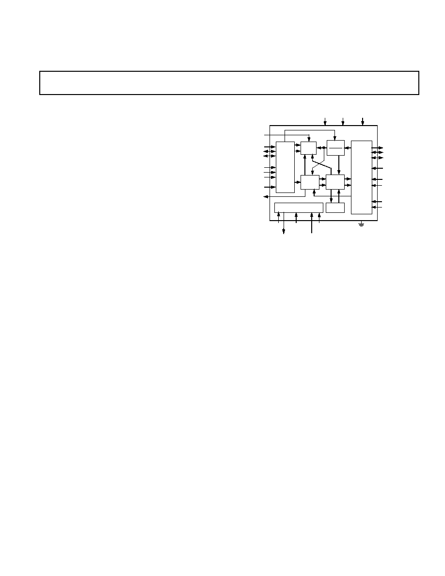
- FUNCTIONAL BLOCK DIAGRAM
- SPECIFICATIONS
- TIMING DIAGRAMS
- TEMPERATURE RANGE
- ABSOLUTE MAXIMUM RATINGS
- ORDERING GUIDE
- PIN FUNCTION DESCRIPTIONS
- PIN CONFIGURATION
- Typical Performance Characteristics
- PRODUCT OVERVIEW (continued)
- ASRC FUNCTIONAL OVERVIEW
- THEORY OF OPERATION
- THE CONCEPTUAL HIGH INTERPOLATION MODEL
- HARDWARE MODEL
- THE SAMPLE RATE CONVERTER ARCHITECTURE
- OPERATING FEATURES
- RESET and Power-Down
- Power Supply and Voltage Reference
- Digital Filter Group Delay
- Mute Control
- Master Clock
- Serial Data PortsÑData Format
- TDM MODE APPLICATION
- Serial Data Port Master Clock Modes
- Bypass Mode
- OUTLINE DIMENSIONS
- Revision History
REV. B
Information furnished by Analog Devices is believed to be accurate and
reliable. However, no responsibility is assumed by Analog Devices for its
use, nor for any infringements of patents or other rights of third parties that
may result from its use. No license is granted by implication or otherwise
under any patent or patent rights of Analog Devices.
a
One Technology Way, P.O. Box 9106, Norwood, MA 02062-9106, U.S.A.
Tel: 781/329-4700
www.analog.com
Fax: 781/326-8703
© Analog Devices, Inc., 2002
AD1895
*
192 kHz Stereo Asynchronous
Sample Rate Converter
FUNCTIONAL BLOCK DIAGRAM
VDD_IO VDD_CORE
SERIAL
INPUT
FIFO
FS
OUT
FS
IN
SERIAL
OUTPUT
DIGITAL
PLL
FIR
FILTER
CLOCK DIVIDER
ROM
AD1895
BYPASS
MUTE_OUT
MUTE_IN
SDATA_I
SCLK_I
LRCLK_I
SMODE_IN_0
SMODE_IN_1
SMODE_IN_2
MCLK_IN
MCLK_OUT
MMODE_0
MMODE_2
MMODE_1
WLNGTH_OUT_0
WLNGTH_OUT_1
SMODE_OUT_0
SMODE_OUT_1
TDM_IN
SDATA_O
SCLK_O
LRCLK_O
RESET
PRODUCT OVERVIEW
The AD1895 is a 24-bit, high performance, single-chip, second
generation asynchronous sample rate converter. Based upon
Analog Devices' experience with its first asynchronous sample
rate converter, the AD1890, the AD1895 offers improved perfor-
mance and additional features. This improved performance
includes a THD + N range of ≠115 dB to ≠122 dB depending
on sample rate and input frequency, 128 dB (A-Weighted)
dynamic range, 192 kHz sampling frequencies for both input and
output sample rates, improved jitter rejection, and 1:8 upsampling
and 7.75:1 downsampling ratios. Additional features include
more serial formats, a bypass mode, and better interfacing to
digital signal processors.
The AD1895 has a 3-wire interface for the serial input and
output ports that supports left-justified, I
2
S, and right-justified
(16-, 18-, 20-, 24-bit) modes. Additionally, the serial output
port supports TDM Mode for daisy-chaining multiple AD1895s to
a digital signal processor. The serial output data is dithered down
to 20, 18, or 16 bits when 20-, 18-, or 16-bit output data is
selected. The AD1895 sample rate converts the data from the
serial input port to the sample rate of the serial output port. The
sample rate at the serial input port can be asynchronous with
respect to the output sample rate of the output serial port. The
master clock to the AD1895, MCLK, can be asynchronous to
both the serial input and output ports.
MCLK can either be generated off-chip or on-chip by the AD1895
master clock oscillator. Since MCLK can be asynchronous to the
input or output serial ports, a crystal can be used to generate
MCLK internally to reduce noise and EMI emissions on the
board. When MCLK is synchronous to either the output or input
serial port, the AD1895 can be configured in a master mode where
MCLK is divided down and used to generate the left/right
and bit clocks for the serial port that is synchronous to MCLK.
The AD1895 supports master modes of 256
◊ f
S
, 512
◊ f
S
, and
768
◊ f
S
for both input and output serial ports.
Conceptually, the AD1895 interpolates the serial input data by
a rate of 2
20
and samples the interpolated data stream by the
output sample rate. In practice, a 64-tap FIR filter with 2
20
polyphases, a FIFO, a digital servo loop that measures the time
difference between input and output samples within 5 ps, and a
digital circuit to track the sample rate ratio are used to perform
the interpolation and output sampling. Refer to the Theory of
Operation section. The digital servo loop and sample rate ratio
circuit automatically track the input and output sample rates.
(continued on page 15)
FEATURES
Automatically Senses Sample Frequencies
No Programming Required
Attenuates Sample Clock Jitter
3.3 V to 5 V Input and 3.3 V Core Supply Voltages
Accepts 16-/18-/20-/24-Bit Data
Up to 192 kHz Sample Rate
Input/Output Sample Ratios from 7.75:1 to 1:8
Bypass Mode
Multiple AD1895 TDM Daisy-Chain Mode
128 dB Signal-to-Noise and Dynamic Range
(A-Weighted, 20 Hz to 20 kHz BW)
Up to ≠122 dB THD + N
Linear Phase FIR Filter
Hardware Controllable Soft Mute
Supports 256 f
S
, 512 f
S
, or 768 f
S
Master Mode
Clock
Flexible 3-Wire Serial Data Port with Left-Justified,
I
2
S, Right-Justified (16-, 18-, 20-, 24-Bit), and TDM
Serial Port Modes
Master/Slave Input and Output Modes
28-Lead SSOP Plastic Package
APPLICATIONS
Home Theater Systems, Automotive Audio Systems,
DVD, DVD-R, CD-R, Set-Top Boxes, Digital Audio
Effects Processors
*Patents pending.
REV. B
≠2≠
AD1895≠SPECIFICATIONS
TEST CONDITIONS, UNLESS OTHERWISE NOTED.
Supply Voltages
VDD_CORE . . . . . . . . . . . . . . . . . . . . . . . . . . . . . . . . . . 3.3 V
VDD_IO . . . . . . . . . . . . . . . . . . . . . . . . . . . . . . 5.0 V or 3.3 V
Ambient Temperature . . . . . . . . . . . . . . . . . . . . . . . . . . . . . . 25
∞C
Input Clock . . . . . . . . . . . . . . . . . . . . . . . . . . . . . . . . . . 30.0 MHz
Input Signal . . . . . . . . . . . . . . . . . . . . . . . . . . 1.000 kHz, 0 dBFS
Measurement Bandwidth . . . . . . . . . . . . . . . . . . 20 to f
S_OUT
/2 Hz
Word Width . . . . . . . . . . . . . . . . . . . . . . . . . . . . . . . . . . . 24 Bits
Load Capacitance . . . . . . . . . . . . . . . . . . . . . . . . . . . . . . . . 50 pF
Input Voltage High . . . . . . . . . . . . . . . . . . . . . . . . . . . . . . . 2.4 V
Input Voltage Low . . . . . . . . . . . . . . . . . . . . . . . . . . . . . . . . 0.8 V
DIGITAL PERFORMANCE (VDD_CORE = 3.3 V
5%, VDD_IO = 5.0 V 10%)
Parameter
Min
Typ
Max
Unit
RESOLUTION
24
Bits
SAMPLE RATE @ MCLK_IN = 30 MHz
6
215
kHz
SAMPLE RATE (@ OTHER MASTER CLOCKS)
1
MCLK_IN/5000
f
S_MAX
< MCLK_IN/138
kHz
SAMPLE RATE RATIOS
Upsampling
1:8
Downsampling
7.75:1
DYNAMIC RANGE
2
(20 Hz to f
S_OUT
/2, 1 kHz, ≠60 dBFS Input) A-Weighted
44.1 kHz: 48 kHz
128
dB
48 kHz: 44.1 kHz
128
dB
48 kHz: 96 kHz
128
dB
44.1 kHz: 192 kHz
128
dB
96 kHz: 48 kHz
127
dB
192 kHz: 32 kHz
127
dB
(20 Hz to f
S_OUT
/2, 1 kHz, ≠60 dBFS Input) No Filter
44.1 kHz: 48 kHz
125
dB
48 kHz: 44.1 kHz
125
dB
48 kHz: 96 kHz
125
dB
44.1 kHz: 192 kHz
125
dB
96 kHz: 48 kHz
124
dB
192 kHz: 32 kHz
124
dB
TOTAL HARMONIC DISTORTION + NOISE
2
(20 Hz to f
S_OUT
/2, 1 kHz, 0 dBFS Input) No Filter
Worst-Case (48 kHz: 96 kHz)
3
≠115
dB
44.1 kHz: 48 kHz
≠120
dB
48 kHz: 44.1 kHz
≠119
dB
48 kHz: 96 kHz
≠118
dB
44.1 kHz: 192 kHz
≠120
dB
96 kHz: 48 kHz
≠122
dB
192 kHz: 32 kHz
≠122
dB
INTERCHANNEL GAIN MISMATCH
0.0
dB
INTERCHANNEL PHASE DEVIATION
0.0
Degrees
MUTE ATTENUATION (24 BITS WORD WIDTH)(A-WEIGHT)
≠127
dB
NOTES
1
Lower sampling rates than those given by this formula are possible, but the jitter rejection will decrease.
2
Refer to the Typical Performance Characteristics section for DNR and THD + N numbers over a wide range of input and output sample rates.
3
For any other ratio, minimum THD + N will be better than ≠115 dB. Please refer to detailed performance plots.
Specifications subject to change without notice.

REV. B
≠3≠
AD1895
DIGITAL TIMING (≠40 C < T
A
< +105 C, VDD_CORE = 3.3 V
5%, VDD_IO = 5.0 V 10%)
Parameter
1
Min
Max
Unit
t
MCLKI
MCLK_IN Period
33.3
ns
f
MCLK
MCLK_IN Frequency
30.0
2, 3
MHz
t
MPWH
MCLK_IN Pulsewidth High
9
ns
t
MPWL
MCLK_IN Pulsewidth Low
12
ns
INPUT SERIAL PORT TIMING
t
LRIS
LRCLK_I Setup to SCLK_I
8
ns
t
SIH
SCLK_I Pulsewidth High
8
ns
t
SIL
SCLK_I Pulsewidth Low
8
ns
t
DIS
SDATA_I Setup to SCLK_I Rising Edge
8
ns
t
DIH
SDATA_I Hold from SCLK_I Rising Edge
3
ns
OUTPUT SERIAL PORT TIMING
t
TDMS
TDM_IN Setup to SCLK_O Falling Edge
3
ns
t
TDMH
TDM_IN Hold from SCLK_O Falling Edge
3
ns
t
DOPD
SDATA_O Propagation Delay from SCLK_O, LRCLK_O
20
ns
t
DOH
SDATA_O Hold from SCLK_O
3
ns
t
LROS
LRCLK_O Setup to SCLK_O (TDM Mode Only)
5
ns
t
LROH
LRCLK_O Hold from SCLK_O (TDM Mode Only)
3
ns
t
SOH
SCLK_O Pulsewidth High
10
ns
t
SOL
SCLK_O Pulsewidth Low
5
ns
t
RSTL
RESET Pulsewidth Low
200
ns
NOTES
1
Refer to Timing Diagrams section.
2
The maximum possible sample rate is: FS
MAX
= f
MCLK
/138.
3
f
MCLK
of up to 34 MHz is possible under the following conditions: 0
∞C < T
A
< 70
∞C, 45/55 or better MCLK_IN duty cycle.
Specifications subject to change without notice.
TIMING DIAGRAMS
t
LRIS
t
SIH
t
DIS
t
SIL
t
DIH
t
LROS
t
SOH
t
DOPD
t
SOL
t
DOH
t
LROH
t
TDMS
t
TDMH
LRCLK_I
SCLK I
SDATA I
LRCLK O
SCLK O
SDATA O
LRCLK O
SCLK O
TDM IN
Figure 1. Input and Output Serial Port Timing (SCLK_I/O,
LRCLK_I/O, SDATA_I/O, TDM_IN)
t
RSTL
MCLK IN
RESET
Figure 2.
RESET Timing
t
MPWH
t
MPWL
Figure 3. MCLK_IN Timing

REV. B
AD1895
≠4≠
DIGITAL FILTERS (VDD_CORE = 3.3 V
5%, VDD_IO = 5.0 V 10%)
Parameter
Min
Typ
Max
Unit
Pass Band
0.4535 f
S_OUT
Hz
Pass-Band Ripple
±0.016
dB
Transition Band
0.4535 f
S_OUT
0.5465 f
S_OUT
Hz
Stop Band
0.5465 f
S_OUT
Hz
Stop-Band Attenuation
≠125
dB
Group Delay
Refer to the Group Delay Equations Section
Specifications subject to change without notice.
DIGITAL I/O CHARACTERISTICS (VDD_CORE = 3.3 V
5%, VDD_IO = 5.0 V 10%)
Parameter
Min
Typ
Max
Unit
Input Voltage High (V
IH
)
2.4
V
Input Voltage Low (V
IL
)
0.8
V
Input Leakage (I
IH
@ V
IH
= 5 V)
+2
µA
Input Leakage (I
IL
@ V
IL
= 0 V)
≠2
µA
Input Capacitance
5
10
pF
Output Voltage High (V
OH
@ I
OH
= ≠4 mA)
VDD_CORE ≠ 0.5
VDD_CORE ≠ 0.4
V
Output Voltage Low (V
OL
@ I
OL
= +4 mA)
0.2
0.5
V
Output Source Current High (I
OH
)
≠4
mA
Output Sink Current Low (I
OL
)
+4
mA
Specifications subject to change without notice.
POWER SUPPLIES
Parameter
Min
Typ
Max
Unit
SUPPLY VOLTAGE
VDD_CORE
3.135
3.3
3.465
V
VDD_IO
*
VDD_CORE
3.3/5.0
5.5
V
ACTIVE SUPPLY CURRENT
I_CORE_ACTIVE
48 kHz: 48 kHz
20
mA
96 kHz: 96 kHz
26
mA
192 kHz: 192 kHz
43
mA
I_IO_ACTIVE
2
mA
POWER-DOWN SUPPLY CURRENT: (ALL CLOCKS STOPPED)
I_CORE_PWRDN
0.5
mA
I_IO_PWRDN
10
µA
*For 3.3 V tolerant inputs, VDD_IO supply should be set to 3.3 V; however, VDD_CORE supply voltage should not exceed VDD_IO.
Specifications subject to change without notice.
≠SPECIFICATIONS

REV. B
≠5≠
AD1895
CAUTION
ESD (electrostatic discharge) sensitive device. Electrostatic charges as high as 4000 V readily
accumulate on the human body and test equipment and can discharge without detection. Although
the AD1895 features proprietary ESD protection circuitry, permanent damage may occur on
devices subjected to high energy electrostatic discharges. Therefore, proper ESD precautions are
recommended to avoid performance degradation or loss of functionality.
WARNING!
ESD SENSITIVE DEVICE
POWER SUPPLIES (VDD_CORE = 3.3 V
5%, VDD_IO = 5.0 V 10%)
Parameter
Min
Typ
Max
Unit
TOTAL ACTIVE POWER DISSIPATION
48 kHz: 48 kHz
65
mW
96 kHz: 96 kHz
85
mW
192 kHz: 192 kHz
132
mW
TOTAL POWER-DOWN DISSIPATION (RESET LOW)
2
mW
Specifications subject to change without notice.
TEMPERATURE RANGE
Parameter
Min
Typ
Max
Unit
Specifications Guaranteed
25
∞C
Functionality Guaranteed
≠40
+105
∞C
Storage
≠55
+150
∞C
Thermal Resistance,
JA
(Junction to Ambient)
109
∞C/W
Specifications subject to change without notice.
ABSOLUTE MAXIMUM RATINGS
*
Parameter
Min
Max
Unit
POWER SUPPLIES
VDD_CORE
≠0.3
+3.6
V
VDD_IO
≠0.3
+6.0
V
DIGITAL INPUTS
Input Current
±10
mA
Input Voltage
DGND ≠ 0.3
VDD_IO + 0.3
V
AMBIENT TEMPERATURE (OPERATING)
≠40
+105
∞C
*Stresses greater than those listed under Absolute Maximum Ratings may cause permanent damage to the device. This is a stress rating only; functional operation of the
device at these or any other conditions above those indicated in the operational section of this specification is not implied. Exposure to absolute maximum rating conditions
for extended periods may affect device reliability.
ORDERING GUIDE
Model
Temperature Range
Package Description
Package Option
AD1895AYRS
≠40
∞C to +105∞C
28-Lead SSOP
RS-28
AD1895AYRSRL
≠40
∞C to +105∞C
28-Lead SSOP
RS-28 on 13" Reel

REV. B
AD1895
≠6≠
PIN FUNCTION DESCRIPTIONS
Pin No.
IN/OUT (I/O)
Mnemonic
Description
1
IN
NC
No Connect
2
IN
MCLK_IN
Master Clock or Crystal Input
3
OUT
MCLK_OUT
Master Clock Output or Crystal Output
4
IN
SDATA_I
Input Serial Data (at Input Sample Rate)
5
IN/OUT
SCLK_I
Master/Slave Input Serial Bit Clock
6
IN/OUT
LRCLK_I
Master/Slave Input Left/Right Clock
7
IN
VDD_IO
3.3 V/5 V Input/Output Digital Supply Pin
8
IN
DGND
Digital Ground Pin
9
IN
BYPASS
ASRC Bypass Mode, Active High
10
IN
SMODE_IN_0
Input Port Serial Interface Mode Select Pin 0
11
IN
SMODE_IN_1
Input Port Serial Interface Mode Select Pin 1
12
IN
SMODE_IN_2
Input Port Serial Interface Mode Select Pin 2
13
IN
RESET
Reset Pin, Active Low
14
IN
MUTE_IN
Mute Input Pin--Active High Normally Connected to MUTE_OUT
15
OUT
MUTE_OUT
Output Mute Control--Active High
16
IN
WLNGTH_OUT_1
Hardware Selectable Output Wordlength--Select Pin 1
17
IN
WLNGTH_OUT_0
Hardware Selectable Output Wordlength--Select Pin 0
18
IN
SMODE_OUT_1
Output Port Serial Interface Mode Select Pin 1
19
IN
SMODE_OUT_0
Output Port Serial Interface Mode Select Pin 0
20
IN
TDM_IN
Serial Data Input
* (Only for Daisy-Chain Mode). Ground when not used.
21
IN
DGND
Digital Ground Pin
22
IN
VDD_CORE
3.3 V Digital Supply Pin
23
OUT
SDATA_O
Output Serial Data (at Output Sample Rate)
24
IN/OUT
LRCLK_O
Master/Slave Output Left/Right Clock
25
IN/OUT
SCLK_O
Master/Slave Output Serial Bit Clock
26
IN
MMODE_0
Master/Slave Clock Ratio Mode Select Pin 0
27
IN
MMODE_1
Master/Slave Clock Ratio Mode Select Pin 1
28
IN
MMODE_2
Master/Slave Clock Ratio Mode Select Pin 2
*Also used to input matched-phase mode data.
PIN CONFIGURATION
28
27
26
25
24
23
22
21
20
19
18
17
16
15
1
2
3
4
5
6
7
8
9
10
11
12
13
14
AD1895
TOP VIEW
(NOT TO SCALE
)
MUTE_IN
RESET
SMODE_IN_2
SMODE_IN_1
SMODE_IN_0
BYPASS
DGND
NC
MCLK_IN
MCLK_OUT
SDATA_I
VDD_IO
LRCLK_I
SCLK_I
MUTE_OUT
WLNGTH_OUT_1
WLNGTH_OUT_0
SMODE_OUT_1
SMODE_OUT_0
TDM_IN
DGND
MMODE_2
MMODE_1
MMODE_0
SCLK_O
VDD_CORE
SDATA_O
LRCLK_O
NC = NO CONNECT
REV. B
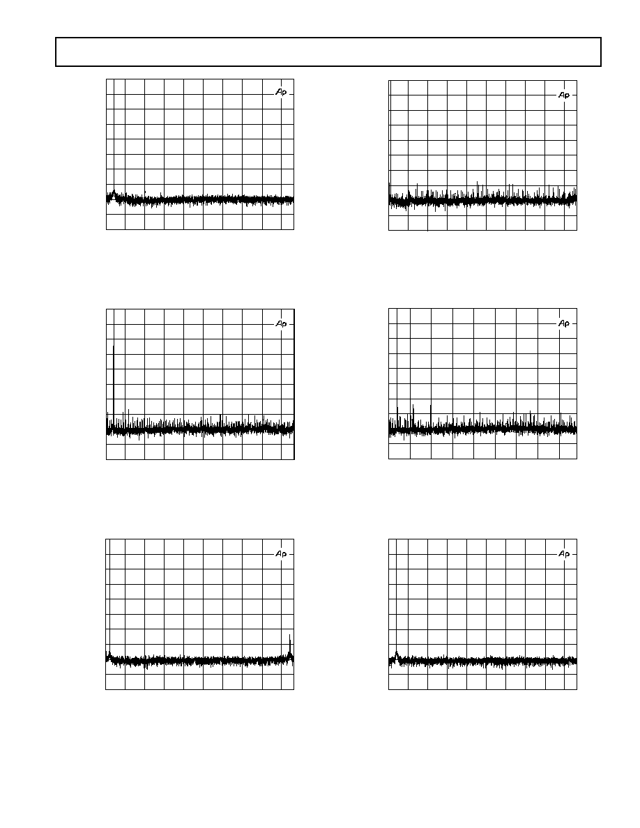
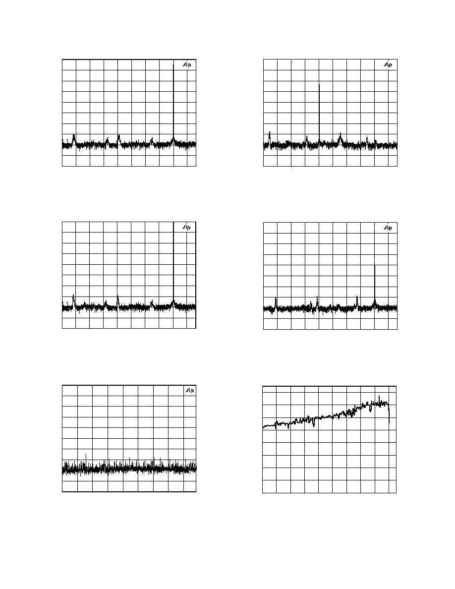
Typical Performance Characteristics≠AD1895
FREQUENCY ≠ kHz
≠200
0
10
20
30
40
50
60
70
80
90
≠180
≠160
≠140
≠120
≠100
≠80
≠60
≠40
≠20
0
dBFS
TPC 4. Wideband FFT Plot (16 k Points) 44.1 kHz: 192 kHz,
0 dBFS 1 kHz Tone
FREQUENCY ≠ kHz
≠200
0
2.5
dBFS
5.0
7.5
10.0
12.5
15.0
17.5
20.0
≠180
≠160
≠140
≠120
≠100
≠80
≠60
≠40
≠20
0
TPC 5. Wideband FFT Plot (16 k Points) 48 kHz: 44.1 kHz,
0 dBFS 1 kHz Tone
FREQUENCY ≠ kHz
≠200
dBFS
≠180
≠160
≠140
≠120
≠100
≠80
≠60
≠40
≠20
0
0
2.5
5.0
7.5
10.0
12.5
15.0
17.5
20.0
22.5
TPC 6. Wideband FFT Plot (16 k Points) 96 kHz: 48 kHz,
0 dBFS 1 kHz Tone
FREQUENCY ≠ kHz
≠200
dBFS
≠180
≠160
≠140
≠120
≠100
≠80
≠60
≠40
≠20
0
0
2.5
5.0
7.5
10.0
12.5
15.0
17.5
20.0
22.5
TPC 1. Wideband FFT Plot (16 k Points) 0 dBFS 1 kHz
Tone, 48 kHz: 48 kHz (Asynchronous)
FREQUENCY ≠ kHz
≠200
0
2.5
dBFS
5.0
7.5
10.0
12.5
15.0
17.5
20.0
22.5
≠180
≠160
≠140
≠120
≠100
≠80
≠60
≠40
≠20
0
TPC 2. Wideband FFT Plot (16 k Points) 0 dBFS 1 kHz
Tone, 44.1 kHz: 48 kHz (Asynchronous)
FREQUENCY ≠ kHz
≠200
0
5
dBFS
10
15
20
25
30
35
40
45
≠180
≠160
≠140
≠120
≠100
≠80
≠60
≠40
≠20
0
TPC 3. Wideband FFT Plot (16 k Points) 48 kHz: 96 kHz,
0 dBFS 1 kHz Tone
≠7≠
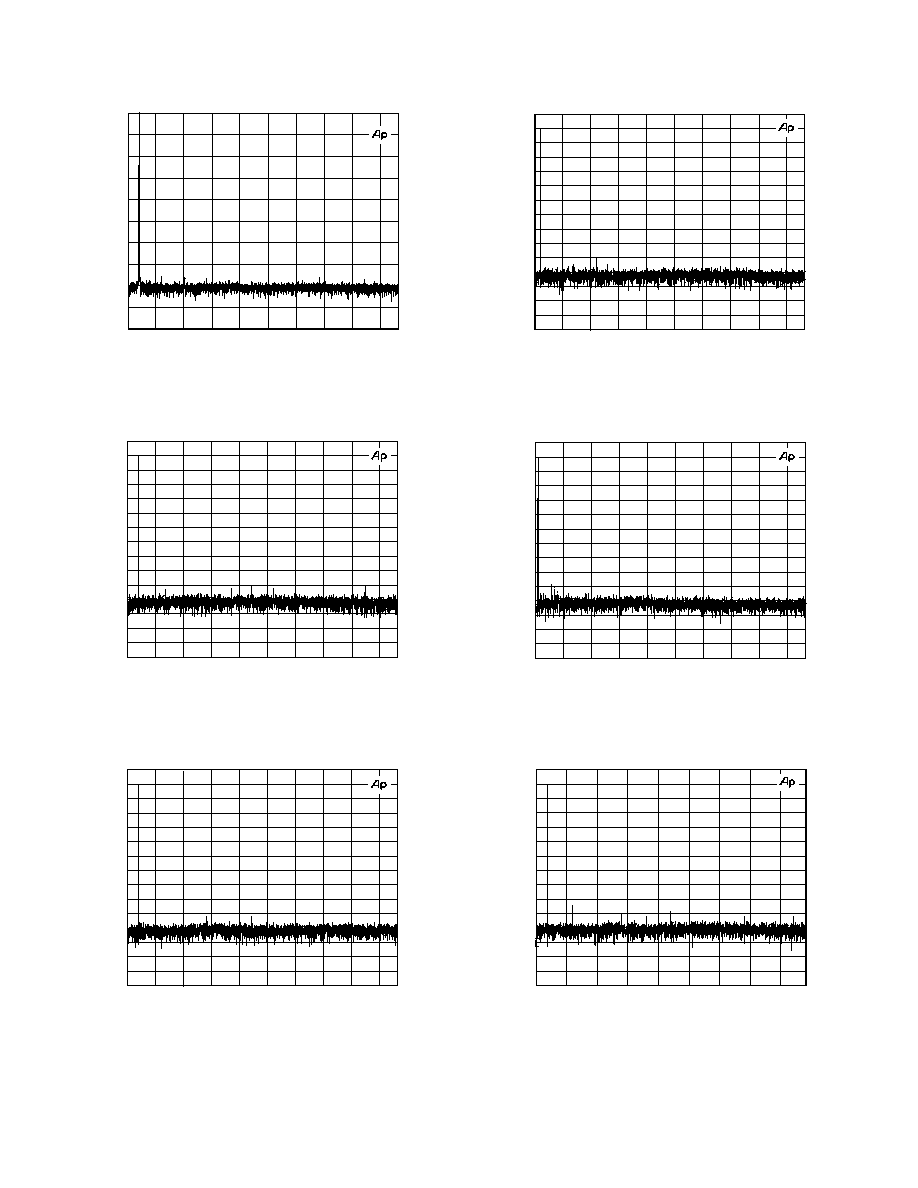
REV. B
AD1895
≠8≠
FREQUENCY ≠ kHz
≠200
dBFS
≠180
≠160
≠140
≠120
≠100
≠80
≠60
≠40
≠20
0
0
2.5
5.0
7.5
10.0
12.5
15.0
17.5
20.0
22.5
TPC 7. Wideband FFT Plot (16 k Points) 192 kHz: 48 kHz,
0 dBFS 1 kHz Tone
FREQUENCY ≠ kHz
≠200
dBFS
≠180
≠160
≠140
≠120
≠100
≠80
≠60
0
2.5
5.0
7.5
10.0
12.5
15.0
17.5
20.0
22.5
≠190
≠170
≠150
≠130
≠110
≠90
≠70
≠50
TPC 8. Wideband FFT Plot (16 k Points) 48 kHz: 48 kHz
≠60 dBFS 1 kHz Tone (Asynchronous)
FREQUENCY ≠ kHz
≠200
dBFS
≠180
≠160
≠140
≠120
≠100
≠80
≠60
0
2.5
5.0
7.5
10.0
12.5
15.0
17.5
20.0
22.5
≠190
≠170
≠150
≠130
≠110
≠90
≠70
≠50
TPC 9. Wideband FFT Plot (16 k Points) 44.1 kHz: 48 kHz,
≠60 dBFS 1 kHz Tone
FREQUENCY ≠ kHz
0
5
10
15
20
25
30
35
40
45
≠200
dBFS
≠180
≠160
≠140
≠120
≠100
≠80
≠60
≠190
≠170
≠150
≠130
≠110
≠90
≠70
≠50
TPC 10. Wideband FFT Plot (16 k Points) 48 kHz: 96 kHz,
≠60 dBFS 1 kHz Tone
FREQUENCY ≠ kHz
≠200
dBFS
≠180
≠160
≠140
≠120
≠100
≠80
≠60
0
10
20
30
40
≠190
≠170
≠150
≠130
≠110
≠90
≠70
≠50
50
60
70
80
90
TPC 11. Wideband FFT Plot (16 k Points) 44.1 kHz: 192 kHz,
≠60 dBFS 1 kHz Tone
≠200
dBFS
≠180
≠160
≠140
≠120
≠100
≠80
≠60
≠190
≠170
≠150
≠130
≠110
≠90
≠70
≠50
FREQUENCY ≠ kHz
0
2.5
5.0
7.5
10.0
12.5
15.0
17.5
20.0
TPC 12. Wideband FFT Plot (16 k Points) 48 kHz: 44.1 kHz,
≠60 dBFS 1 kHz Tone

REV. B
AD1895
≠9≠
FREQUENCY ≠ kHz
≠200
dBFS
≠180
≠160
≠140
≠120
≠100
≠80
≠60
0
2.5
5.0
7.5
10.0
≠190
≠170
≠150
≠130
≠110
≠90
≠70
≠50
12.5
15.0
17.5
20.0
22.5
TPC 13. Wideband FFT Plot (16 k Points) 96 kHz: 48 kHz,
≠60 dBFS 1 kHz Tone
FREQUENCY ≠ kHz
≠200
dBFS
≠180
≠160
≠140
≠120
≠100
≠80
≠60
0
2.5
5.0
7.5
10.0
≠190
≠170
≠150
≠130
≠110
≠90
≠70
≠50
12.5
15.0
17.5
20.0
22.5
TPC 14. Wideband FFT Plot (16 k Points) 192 kHz: 48 kHz,
≠60 dBFS 1 kHz Tone
FREQUENCY ≠ kHz
dBFS
≠180
≠160
≠140
≠120
≠100
≠80
≠60
0
2.5
5.0
7.5
10.0
12.5
15.0
17.5
20.0
22.5
≠40
≠20
0
TPC 15. IMD, 10 kHz and 11 kHz, 0 dBFS Tone,
44:1 kHz: 48 kHz
FREQUENCY ≠ kHz
dBFS
≠180
≠160
≠140
≠120
≠100
≠80
≠60
0
2.5
5.0
7.5
10.0
12.5
15.0
17.5
20.0
22.5
≠40
≠20
0
TPC 16. IMD, 10 kHz and 11 kHz, 0 dBFS Tone,
96 kHz: 48 kHz
FREQUENCY ≠ kHz
0
2.5
dBFS
5.0
7.5
10.0
≠180
≠160
≠140
≠120
≠100
≠80
≠60
12.5
15.0
17.5
20.0
≠40
≠20
0
TPC 17. IMD, 10 kHz and 11 kHz, 0 dBFS Tone,
48 kHz: 44.1 kHz
FREQUENCY ≠ kHz
≠200
dBFS
≠180
≠160
≠140
≠120
≠100
≠80
≠60
0
2.5
5.0
7.5
10.0
12.5
15.0
17.5
20.0
22.5
≠40
≠20
0
TPC 18. Wideband FFT Plot (16 k Points) 44.1 kHz: 48 kHz,
0 dBFS 20 kHz Tone
REV. B
AD1895
≠10≠
FREQUENCY ≠ kHz
≠200
dBFS
≠180
≠160
≠140
≠120
≠100
≠80
≠60
0
10
20
30
40
50
60
70
80
90
≠40
≠20
0
TPC 19. Wideband FFT Plot (16 k Points) 192 kHz: 192 kHz,
0 dBFS 80 kHz Tone
FREQUENCY ≠ kHz
≠200
dBFS
≠180
≠160
≠140
≠120
≠100
≠80
≠60
0
2.5
5.0
7.5
10.0
12.5
15.0
17.5
20.0
22.5
≠40
≠20
0
TPC 20. Wideband FFT Plot (16 k Points) 48 kHz: 48 kHz,
0 dBFS 20 kHz Tone
FREQUENCY ≠ kHz
≠200
0
2.5
dBFS
5.0
7.5
10.0
≠180
≠160
≠140
≠120
≠100
≠80
≠60
12.5
15.0
17.5
20.0
≠40
≠20
0
TPC 21. Wideband FFT Plot (16 k Points) 48 kHz: 44:1 kHz,
0 dBFS 20 kHz Tone
FREQUENCY ≠ kHz
≠200
dBFS
≠180
≠160
≠140
≠120
≠100
≠80
≠60
0
5
10
15
20
25
30
35
40
45
≠40
≠20
0
TPC 22. Wideband FFT Plot (16 k Points) 48 kHz: 96 kHz,
0 dBFS 20 kHz Tone
FREQUENCY ≠ kHz
≠200
dBFS
≠180
≠160
≠140
≠120
≠100
≠80
≠60
0
2.5
5.0
7.5
10.0
12.5
15.0
17.5
20.0
22.5
≠40
≠20
0
TPC 23. Wideband FFT Plot (16 k Points) 96 kHz: 48 kHz,
0 dBFS 20 kHz Tone
OUTPUT SAMPLE RATE ≠ Hz
30000
≠135
THD + N ≠ dBFS
48000
66000
102000
138000
≠133
≠131
≠129
≠127
≠125
≠123
≠121
≠119
84000
120000
156000
174000
192000
TPC 24. THD + N vs. Output Sample Rate, f
S_IN
= 192 kHz,
0 dBFS 1 kHz Tone

REV. B
AD1895
≠11≠
OUTPUT SAMPLE RATE ≠ Hz
30000
≠135
THD + N ≠ dBFS
48000
66000
102000
138000
≠133
≠131
≠129
≠127
≠125
≠123
≠121
≠119
84000
120000
156000
174000
192000
TPC 25. THD + N vs. Output Sample Rate, f
S_IN
= 48 kHz,
0 dBFS 1 kHz Tone
OUTPUT SAMPLE RATE ≠ Hz
30000
≠135
THD + N ≠ dBFS
48000
66000
102000
138000
≠133
≠131
≠129
≠127
≠125
≠123
≠121
≠119
84000
120000
156000
174000
192000
TPC 26. THD + N vs. Output Sample Rate, f
S_IN
=
44.1 kHz, 0 dBFS 1 kHz Tone
OUTPUT SAMPLE RATE ≠ Hz
30000
≠135
THD + N ≠ dBFS
48000
66000
102000
138000
≠133
≠131
≠129
≠127
≠125
≠123
≠121
≠119
84000
120000
156000
174000
192000
TPC 27. THD + N vs. Output Sample Rate, f
S_IN
= 32 kHz,
0 dBFS 1 kHz Tone
OUTPUT SAMPLE RATE ≠ Hz
30000
≠135
THD + N ≠ dBFS
48000
66000
102000
138000
≠133
≠131
≠129
≠127
≠125
≠123
≠121
≠119
84000
120000
156000
174000
192000
TPC 28. THD + N vs. Output Sample Rate, f
S_IN
= 96 kHz,
0 dBFS 1 kHz Tone
OUTPUT SAMPLE RATE ≠ Hz
30000
≠135
DNR ≠ dBFS
48000
66000
102000
138000
≠133
≠131
≠129
≠127
≠125
≠123
≠121
≠119
84000
120000
156000
174000
192000
TPC 29. DNR (Unweighted) vs. Output Sample Rate,
f
S_IN
= 192 kHz, ≠60 dBFS 1 kHz Tone
OUTPUT SAMPLE RATE ≠ Hz
30000
≠135
DNR ≠ dBFS
48000
66000
102000
138000
≠133
≠131
≠129
≠127
≠125
≠123
≠121
≠119
84000
120000
156000
174000
192000
TPC 30. DNR (Unweighted) vs. Output Sample Rate,
f
S_IN
= 32 kHz, ≠60 dBFS 1 kHz Tone

REV. B
AD1895
≠12≠
OUTPUT SAMPLE RATE ≠ Hz
30000
≠135
DNR ≠ dBFS
48000
66000
102000
138000
≠133
≠131
≠129
≠127
≠125
≠123
≠121
≠119
84000
120000
156000
174000
192000
TPC 31. DNR (Unweighted) vs. Output Sample Rate,
f
S_IN
= 96 kHz, ≠60 dBFS 1 kHz Tone
FREQUENCY ≠ Hz
10000
20000
30000
40000
50000
60000
≠140
dBFS
≠120
≠100
≠80
≠60
≠40
≠20
0
0
192kHz: 96kHz
192kHz: 48kHz
192kHz: 32kHz
TPC 32. Digital Filter Frequency Response
OUTPUT SAMPLE RATE ≠ Hz
30000
≠135
DNR ≠ dBFS
48000
66000
102000
138000
≠133
≠131
≠129
≠127
≠125
≠123
≠121
≠119
84000
120000
156000
174000
192000
TPC 33. DNR (Unweighted) vs. Output Sample Rate,
f
S_IN
= 48 kHz, ≠60 dBFS 1 kHz Tone
OUTPUT SAMPLE RATE ≠ Hz
30000
≠135
DNR ≠ dBFS
48000
66000
102000
138000
≠133
≠131
≠129
≠127
≠125
≠123
≠121
≠119
84000
120000
156000
174000
192000
TPC 34. DNR (Unweighted) vs. Output Sample Rate,
f
S_IN
= 44.1 kHz, ≠60 dBFS 1 kHz Tone
0
FREQUENCY ≠ Hz
4000
8000
12000
≠0.10
dBFS
16000
20000
24000
≠0.09
≠0.08
≠0.07
≠0.06
≠0.05
≠0.04
≠0.03
≠0.02
≠0.01
0.00
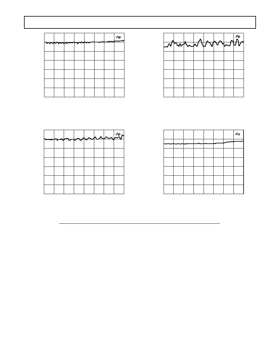
TPC 35. Pass-Band Ripple, 192 kHz: 48 kHz
INPUT LEVEL ≠ dBFS
≠5
≠140
LINEARITY ERR
OR ≠ dBr
≠120
≠100
≠80
≠60
≠40
≠20
0
≠4
≠3
≠2
≠1
0
1
2
3
4
5
TPC 36. Linearity Error, 48 kHz: 48 kHz, 0 dBFS to
≠140 dBFS Input, 200 Hz Tone

REV. B
AD1895
≠13≠
INPUT LEVEL ≠ dBFS
≠5
≠140
LINEARITY ERR
OR ≠ dBr
≠120
≠100
≠80
≠60
≠40
≠20
0
≠4
≠3
≠2
≠1
0
1
2
3
4
5
TPC 37. Linearity Error, 48 kHz: 44.1 kHz, 0 dBFS to
≠140 dBFS Input, 200 Hz Tone
INPUT LEVEL ≠ dBFS
≠5
≠140
LINEARITY ERR
OR ≠ dBr
≠120
≠100
≠80
≠60
≠40
≠20
0
≠4
≠3
≠2
≠1
0
1
2
3
4
5
TPC 38. Linearity Error, 96 kHz: 48 kHz, 0 dBFS to
≠140 dBFS Input, 200 Hz Tone
INPUT LEVEL ≠ dBFS
≠5
≠140
LINEARITY ERR
OR ≠ dBr
≠120
≠100
≠80
≠60
≠40
≠20
0
≠4
≠3
≠2
≠1
0
1
2
3
4
5
TPC 39. Linearity Error, 44.1 kHz: 48 kHz, 0 dBFS to
≠140 dBFS Input, 200 Hz Tone
INPUT LEVEL ≠ dBFS
≠5
≠140
LINEARITY ERR
OR ≠ dBr
≠120
≠100
≠80
≠60
≠40
≠20
0
≠4
≠3
≠2
≠1
0
1
2
3
4
5
TPC 40. Linearity Error, 48 kHz: 96 kHz, 0 dBFS to
≠140 dBFS Input, 200 Hz Tone
INPUT LEVEL ≠ dBFS
≠5
≠140
LINEARITY ERR
OR ≠ dBr
≠120
≠100
≠80
≠60
≠40
≠20
0
≠4
≠3
≠2
≠1
0
1
2
3
4
5
TPC 41. Linearity Error, 44.1 kHz: 192 kHz, 0 dBFS to
≠140 dBFS Input, 200 Hz Tone
INPUT LEVEL ≠ dBFS
≠5
≠140
LINEARITY ERR
OR ≠ dBr
≠120
≠100
≠80
≠60
≠40
≠20
0
≠4
≠3
≠2
≠1
0
1
2
3
4
5
TPC 42. Linearity Error, 192 kHz: 44.1 kHz, 0 dBFS to
≠140 dBFS Input, 200 Hz Tone

REV. B
AD1895
≠14≠
INPUT LEVEL ≠ dBFS
≠140
dBr
≠120
≠100
≠80
≠60
≠40
≠20
0
≠110.0
≠112.5
≠115.0
≠117.5
≠120.0
≠122.5
≠125.0
≠127.5
≠130.0
≠132.5
≠135.0
≠137.5
≠140.0
TPC 43. THD + N vs. Input Amplitude, 48 kHz: 44.1 kHz,
1 kHz Tone
INPUT LEVEL ≠ dBFS
≠140
dBr
≠120
≠100
≠80
≠60
≠40
≠20
0
≠110.0
≠112.5
≠115.0
≠117.5
≠120.0
≠122.5
≠125.0
≠127.5
≠130.0
≠132.5
≠135.0
≠137.5
≠140.0
TPC 44. THD + N vs. Input Amplitude, 96 kHz: 48 kHz,
1 kHz Tone
INPUT LEVEL ≠ dBFS
≠140
dBr
≠120
≠100
≠80
≠60
≠40
≠20
0
≠110.0
≠112.5
≠115.0
≠117.5
≠120.0
≠122.5
≠125.0
≠127.5
≠130.0
≠132.5
≠135.0
≠137.5
≠140.0
TPC 45. THD + N vs. Input Amplitude, 44.1 kHz: 48 kHz,
1 kHz Tone
INPUT LEVEL ≠ dBFS
≠140
dBr
≠120
≠100
≠80
≠60
≠40
≠20
0
≠110.0
≠112.5
≠115.0
≠117.5
≠120.0
≠122.5
≠125.0
≠127.5
≠130.0
≠132.5
≠135.0
≠137.5
≠140.0
TPC 46. THD + N vs. Input Amplitude, 48 kHz: 96 kHz,
1 kHz Tone
INPUT LEVEL ≠ dBFS
≠140
dBr
≠120
≠100
≠80
≠60
≠40
≠20
0
≠110.0
≠112.5
≠115.0
≠117.5
≠120.0
≠122.5
≠125.0
≠127.5
≠130.0
≠132.5
≠135.0
≠137.5
≠140.0
TPC 47. THD + N vs. Input Amplitude, 44.1 kHz: 192 kHz,
1 kHz Tone
INPUT LEVEL ≠ dBFS
≠140
dBr
≠120
≠100
≠80
≠60
≠40
≠20
0
≠110.0
≠112.5
≠115.0
≠117.5
≠120.0
≠122.5
≠125.0
≠127.5
≠130.0
≠132.5
≠135.0
≠137.5
≠140.0
TPC 48. THD + N vs. Input Amplitude, 192 kHz: 48 kHz,
1 kHz Tone
REV. B
AD1895
≠15≠
PRODUCT OVERVIEW
(continued from page 1)
The digital servo loop measures the time difference between
input and output sample rates within 5 ps. This is necessary in
order to select the correct polyphase filter coefficient. The digital
servo loop has excellent jitter rejection for both input and output
sample rates as well as the master clock. The jitter rejection begins
at less than 1 Hz. This requires a long settling time whenever
RESET is deasserted or when the input or output sample rate
changes. To reduce the settling time, upon deassertion of
RESET
or a change in a sample rate, the digital servo loop enters the Fast
Settling Mode. When the digital servo loop has adequately settled
in the Fast Mode, it switches into the Normal or Slow Settling
Mode and continues to settle until the time difference measurement
between input and output sample rates is within 5 ps. During
Fast Mode, the MUTE_OUT signal is asserted high. Normally,
the MUTE_OUT is connected to the MUTE_IN pin. The
MUTE_IN signal is used to softly mute the AD1895 upon
assertion and softly unmute the AD1895 when it is deasserted.
The sample rate converter of the AD1895 can be bypassed
altogether using the Bypass Mode. In Bypass Mode, the AD1895's
serial input data is directly passed to the serial output port with-
out any dithering. This is useful for passing through nonaudio
data or when the input and output sample rates are synchronous
to one another and the sample rate ratio is exactly 1 to 1.
The AD1895 is a 3.3 V, 5 V input tolerant part and is available
in a 28-lead SSOP SMD package. The AD1895 is 5 V input
tolerant only when the VDD_IO supply pin is supplied with 5 V.
FREQUENCY ≠ kHz
≠180
dBr
2.5
5.0
7.5
10.0
12.5
15.0
17.5
≠170
≠160
≠150
≠140
≠130
≠120
≠110
20.0
TPC 49. THD + N vs. Frequency Input, 48 kHz: 44.1 kHz,
0 dBFS
FREQUENCY ≠ kHz
≠180
dBr
2.5
5.0
7.5
10.0
12.5
15.0
17.5
≠170
≠160
≠150
≠140
≠130
≠120
≠110
20.0
TPC 50. THD + N vs. Frequency Input, 44.1 kHz: 48 kHz,
0 dBFS
FREQUENCY ≠ kHz
≠180
dBr
2.5
5.0
7.5
10.0
12.5
15.0
17.5
≠170
≠160
≠150
≠140
≠130
≠120
≠110
20.0
TPC 51. THD + N vs. Frequency Input, 48 kHz: 96 kHz,
0 dBFS
FREQUENCY ≠ kHz
≠180
dBr
2.5
5.0
7.5
10.0
12.5
15.0
17.5
≠170
≠160
≠150
≠140
≠130
≠120
≠110
20.0
TPC 52. THD + N vs. Frequency Input, 96 kHz: 48 kHz,
0 dBFS
REV. B
AD1895
≠16≠
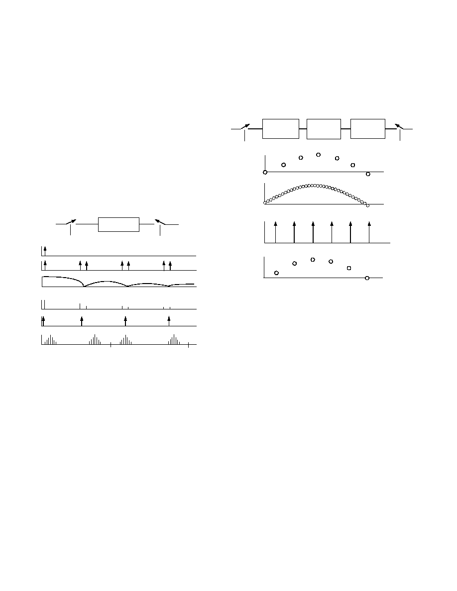
ASRC FUNCTIONAL OVERVIEW
THEORY OF OPERATION
Asynchronous sample rate conversion is converting data from one
clock source at some sample rate to another clock source at the
same or different sample rate. The simplest approach to asyn-
chronous sample rate conversion is the use of a zero-order hold
between two samplers as shown in Figure 4. In an asynchronous
system, T2 is never equal to T1 nor is the ratio between T2 and
T1 rational. As a result, samples at f
S_OUT
will be repeated or
dropped, producing an error in the resampling process. The
frequency domain shows the wide side lobes that result from this
error when the sampling of f
S_OUT
is convolved with the attenuated
images from the sin(x)/x nature of the zero-order hold. The images
at f
S_IN
, dc signal images, of the zero-order hold are infinitely
attenuated. Since the ratio of T2 to T1 is an irrational number,
the error resulting from the resampling at f
S_OUT
can never be
eliminated. However, the error can be significantly reduced
through interpolation of the input data at f
S_IN
. The AD1895 is
conceptually interpolated by a factor of 2
20
.
ZERO-ORDER
HOLD
IN
OUT
f
S_IN
= 1/T1
f
S_OUT
= 1/T2
ORIGINAL SIGNAL
SAMPLED AT
f
S_IN
SIN(X)/X OF ZERO-ORDER HOLD
SPECTRUM OF ZERO-ORDER HOLD OUTPUT
SPECTRUM OF
f
S_OUT
SAMPLING
f
S_OUT
2
f
S_OUT
FREQUENCY RESPONSE OF
f
S_OUT
CONVOLVED WITH ZERO-ORDER
HOLD SPECTRUM
Figure 4. Zero-Order Hold Being Used by f
S_OUT
to
Resample Data from f
S_IN
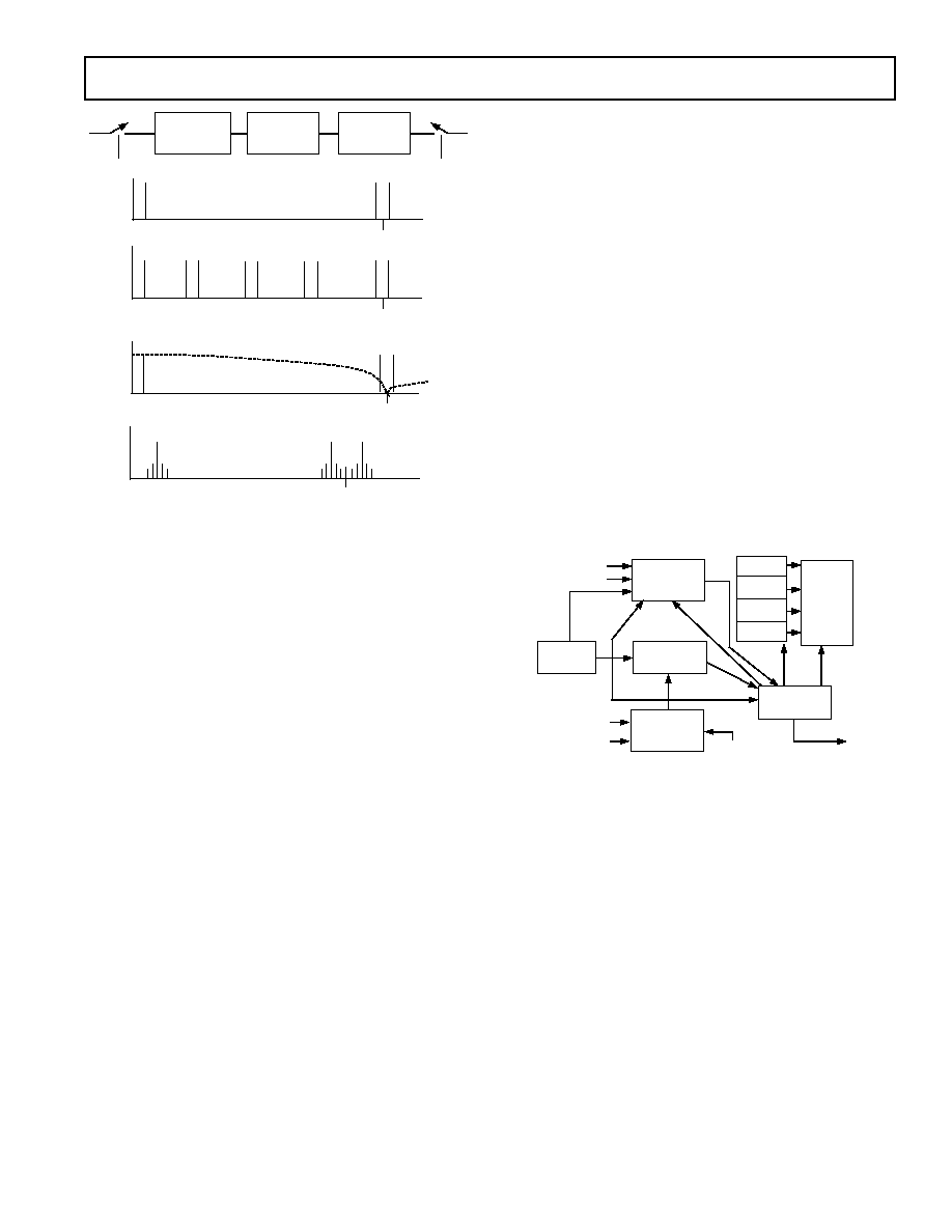
THE CONCEPTUAL HIGH INTERPOLATION MODEL
Interpolation of the input data by a factor of 2
20
involves placing
(2
20
≠1) samples between each f
S_IN
sample. Figure 5 shows
both the time domain and the frequency domain of interpolation
by a factor of 2
20
. Conceptually, interpolation by 2
20
would
involve the steps of zero-stuffing (2
20
≠1) a number of samples
between each f
S_IN
sample and convolving this interpolated signal
with a digital low-pass filter to suppress the images. In the time
domain, it can be seen that f
S_OUT
selects the closest f
S_IN
◊ 2
20
sample from the zero-order hold as opposed to the nearest f
S_IN
sample in the case of no interpolation. This significantly reduces
the resampling error.
IN
OUT
f
S_IN
f
S_OUT
TIME DOMAIN OF
f
S_IN
SAMPLES
TIME DOMAIN OUTPUT OF THE LOW-PASS FILTER
TIME DOMAIN OF
f
S_OUT
RESAMPLING
TIME DOMAIN OF THE ZERO-ORDER HOLD OUTPUT
INTERPOLATE
BY N
LOW-PASS
FILTER
ZERO-ORDER
HOLD
Figure 5. Time Domain of the Interpolation and Resampling
In the frequency domain shown in Figure 6, the interpolation
expands the frequency axis of the zero-order hold. The images
from the interpolation can be sufficiently attenuated by a good
low-pass filter. The images from the zero-order hold are now
pushed by a factor of 2
20
closer to the infinite attenuation point
of the zero-order hold, which is f
S_IN
◊ 2
20
. The images at the
zero-order hold are the determining factor for the fidelity of the
output at f
S_OUT
. The worst-case images can be computed from
the zero-order hold frequency response, maximum image =
sin (
◊ F/f
S_INTERP
)/(
◊ F/f
S_INTERP
). F is the frequency of the
worst-case image, which would be 2
20
◊ f
S_IN
± f
S_IN
/2 , and
f
S_INTERP
is f
S_IN
◊ 2
20
.
The following worst-case images would appear for f
S_IN
=
192 kHz:
Image at f
S_INTERP
≠ 96 kHz = ≠125.1 dB
Image at f
S_INTERP
+ 96 kHz = ≠125.1 dB
REV. B
AD1895
≠17≠
FREQUENCY DOMAIN OF SAMPLES AT
f
S_IN
FREQUENCY DOMAIN OF THE INTERPOLATION
FREQUENCY DOMAIN OF
f
S_OUT
RESAMPLING
FREQUENCY DOMAIN AFTER
RESAMPLING
IN
OUT
f
S_IN
f
S_OUT
INTERPOLATE
BY N
LOW-PASS
FILTER
ZERO-ORDER
HOLD
f
S_IN
2
20
f
S_IN
2
20
f
S_IN
2
20
f
S_IN
SIN(X)/X OF ZERO-ORDER HOLD
Figure 6. Frequency Domain of the Interpolation and
Resampling
HARDWARE MODEL
The output rate of the low-pass filter of Figure 5 would be the
interpolation
rate, 2
20
◊ 192000 kHz = 201.3 GHz. Sampling at
a rate of 201.3 GHz is clearly impractical, not to mention the
number of taps required to calculate each interpolated sample.
However, since interpolation by 2
20
involves zero-stuffing 2
20
≠1
samples between each f
S_IN
sample, most of the multiplies in
the low-pass FIR filter are by zero. A further reduction can be
realized by the fact that since only one interpolated sample is
taken at the output at the f
S_OUT
rate, only one convolution
needs to be performed per f
S_OUT
period instead of 2
20
convo-
lutions. A 64-tap FIR filter for each f
S_OUT
sample is sufficient
to suppress the images caused by the interpolation.
The difficulty with the above approach is that the correct inter-
polated sample needs to be selected upon the arrival of f
S_OUT
.
Since there are 2
20
possible convolutions per f
S_OUT
period, the
arrival of the f
S_OUT
clock must be measured with an accuracy
of 1/201.3 GHz = 4.96 ps. Measuring the f
S_OUT
period with a
clock of 201.3 GHz frequency is clearly impossible; instead,
several coarse measurements of the f
S_OUT
clock period are made
and averaged over time.
Another difficulty with the above approach is the number of
coefficients required. Since there are 2
20
possible convolutions
with a 64-tap FIR filter, there needs to be 2
20
polyphase coeffi-
cients for each tap, which requires a total of 2
26
coefficients. To
reduce the number of coefficients in ROM, the AD1895 stores a
small subset of coefficients and performs a high order interpola-
tion between the stored coefficients. So far, the above approach
works for the case of f
S_OUT
> f
S_IN
. However, in the case when
the output sample rate, f
S_OUT
, is less than the input sample
rate, f
S_IN
, the ROM starting address, input data, and length of
the convolution must be scaled. As the input sample rate rises
over the output sample rate, the antialiasing filter's cutoff fre-
quency has to be lowered because the Nyquist frequency of the
output samples is less than the Nyquist frequency of the input
samples. To move the cutoff frequency of the antialiasing filter,
the coefficients are dynamically altered and the length of the
convolution is increased by a factor of f
S_IN
/f
S_OUT
. This tech-
nique is supported by the Fourier transform property that if f(t)
is F(
), then f(k ◊ t) is F(/k). Thus, the range of decimation is
simply limited by the size of the RAM.
THE SAMPLE RATE CONVERTER ARCHITECTURE
The architecture of the sample rate converter is shown in
Figure 7. The sample rate converter's FIFO block adjusts the
left and right input samples and stores them for the FIR filter's
convolution cycle. The f
S_IN
counter provides the write address to
the FIFO block and the ramp input to the digital servo loop. The
ROM stores the coefficients for the FIR filter convolution and
performs a high order interpolation between the stored coefficients.
The sample rate ratio block measures the sample rate for dynami-
cally altering the ROM coefficients and scaling of the FIR filter
length as well as the input data. The digital servo loop automatically
tracks the f
S_IN
and f
S_OUT
sample rates and provides the RAM
and ROM start addresses for the start of the FIR filter convolution.
RIGHT DATA IN
LEFT DATA IN
FIFO
ROM A
ROM B
ROM C
ROM D
HIGH
ORDER
INTERP
DIGITAL
SERVO LOOP
FIR FILTER
SAMPLE RATE
RATIO
f
S_IN
COUNTER
SAMPLE RATE RATIO
EXTERNAL
RATIO
f
S_IN
f
S_OUT
L/R DATA OUT
Figure 7. Architecture of the Sample Rate Converter
The FIFO receives the left and right input data and adjusts the
amplitude of the data for both the soft muting of the sample rate
converter and the scaling of the input data by the sample rate
ratio before storing the samples in the RAM. The input data
is scaled by the sample rate ratio because as the FIR filter length
of the convolution increases, so does the amplitude of the convo-
lution output. To keep the output of the FIR filter from saturating,
the input data is scaled down by multiplying it by f
S_OUT
/f
S_IN
when f
S_OUT
< f
S_IN
. The FIFO also scales the input data for
muting and unmuting the AD1895.
The RAM in the FIFO is 512 words deep for both left and right
channels. A small offset of 16 is added to the write address
provided by the f
S_IN
counter to prevent the RAM read pointer
from ever overlapping the write address. The maximum deci-
mation rate can be calculated from the RAM word depth as
(512 ≠ 16)/64 taps = 7.75 and a small offset.

REV. B
AD1895
≠18≠
The digital servo loop is essentially a ramp filter that provides
the initial pointer to the address in RAM and ROM for the start
of the FIR convolution. The RAM pointer is the integer output
of the ramp filter, while the ROM is the fractional part. The
digital servo loop must be able to provide excellent rejection of
jitter on the f
S_IN
and f
S_OUT
clocks as well as measure the arrival
of the f
S_OUT
clock within 4.97 ps. The digital servo loop will
also divide the fractional part of the ramp output by the ratio of
f
S_IN
/f
S_OUT
for the case when f
S_IN
> f
S_OUT
, to dynamically alter
the ROM coefficients.
The digital servo loop is implemented with a multirate filter. To
settle the digital servo loop filter quicker upon startup or a change
in the sample rate, a Fast Mode was added to the filter. When
the digital servo loop starts up or the sample rate is changed, the
digital servo loop kicks into Fast Mode to adjust and settle on the
new sample rate. Upon sensing the digital servo loop settling down
to some reasonable value, the digital servo loop will kick into
Normal or Slow Mode. During Fast Mode, the MUTE_OUT
signal of the sample rate converter is asserted to let the user
know that they should mute the sample rate converter to avoid
any clicks or pops. The frequency response of the digital servo
loop for Fast Mode and Slow Mode are shown in Figure 8.
The FIR filter is a 64-tap filter in the case of f
S_OUT
f
S_IN
and is
(f
S_IN
/f
S_OUT
)
◊ 64 taps for the case when f
S_IN
> f
S_OUT
. The FIR
filter performs its convolution by loading in the starting address
of the RAM address pointer and the ROM address pointer
from the digital servo loop at the start of the f
S_OUT
period.
The FIR filter then steps through the RAM by decrementing its
address by 1 for each tap, and the ROM pointer increments its
address by the (f
S_OUT
/f
S_IN
)
◊ 2
20
ratio for f
S_IN
> f
S_OUT
or 2
20
for f
S_OUT
f
S_IN
. Once the ROM address rolls over, the con-
volution is completed. The convolution is performed for both
the left and right channels, and the multiply accumulate circuit
used for the convolution is shared between the channels.
The f
S_IN
/f
S_OUT
sample rate ratio circuit is used to dynamically
alter the coefficients in the ROM for the case when f
S_IN
> f
S_OUT
.
The ratio is calculated by comparing the output of an f
S_OUT
counter to the output of an f
S_IN
counter. If f
S_OUT
> f
S_IN
, the
ratio is held at 1. If f
S_IN
> f
S_OUT
, the sample rate ratio is updated
if it is different by more than two f
S_OUT
periods from the previous
f
S_OUT
to f
S_IN
comparison. This is done to provide some
hysteresis to prevent the filter length from oscillating and causing
distortion.
10
0
≠10
≠20
≠30
≠40
≠50
≠60
≠70
≠80
≠90
≠100
≠110
≠120
≠130
≠140
≠150
≠160
≠170
≠180
≠190
≠200
≠210
≠220
0.01 0.1
1
10
100
1e3
1e4
1e5
FREQUENCY ≠ Hz
SLOW MODE
FAST MODE
Figure 8. Frequency Response of the Digital Servo Loop. f
S_IN
is the x-axis, f
S_OUT
= 192 kHz, master clock
frequency is 30 MHz.

REV. B
AD1895
≠19≠
OPERATING FEATURES
RESET and Power-Down
When
RESET is asserted low, the AD1895 will turn off the
master clock input to the AD1895, MCLK_IN, initialize all of its
internal registers to their default values, and three-state all of the
I/O pins. While
RESET is active low, the AD1895 is consuming
minimum power. For the lowest possible power consumption
while
RESET is active low, all of the input pins to the AD1895
should be static.
When
RESET is deasserted, the AD1895 begins its initialization
routine where all locations in the FIFO are initialized to zero,
MUTE_OUT is asserted high, and any I/O pins configured as
outputs are enabled. The mute control counter, which controls
the soft mute attenuation of the input samples, is initialized to
maximum attenuation, ≠127 dB (see Mute Control section).
When asserting
RESET and deasserting RESET, the RESET
should be held low for a minimum of five MCLK_IN cycles.
During power-up, the
RESET should be held low until the power
supplies have stabilized. It is recommended that the AD1895 be
reset when changing modes.
Power Supply and Voltage Reference
The AD1895 is designed for 3 V operation with 5 V input toler-
ance on the input pins. VDD_CORE is the 3 V supply that is used
to power the core logic of the AD1895 and to drive the output
pins. VDD_IO is used to set the input voltage tolerance of the
input pins. In order for the input pins to be 5 V input tolerant,
VDD_IO must be connected to a 5 V supply. If the input pins do
not have to be 5 V input tolerant, then VDD_IO can be connected
to VDD_CORE. VDD_IO should never be less than VDD_CORE.
VDD_CORE and VDD_IO should be bypassed with 100 nF
ceramic chip capacitors as close to the pins as possible to minimize
power supply and ground bounce caused by inductance in the
traces. A bulk aluminium electrolytic capacitor of 47
µF should
also be provided on the same PC board as the AD1895.
Digital Filter Group Delay
The filter group delay is given by the equation:
GD
f
f
for f
f
GD
f
f
f
f
for f
f
S
IN
S
IN
S
OUT
S
IN
S
IN
S
IN
S
IN
S
OUT
S
OUT
S
IN
=
+
>
=
+
◊
<
16
32
16
32
_
_
_
_
_
_
_
_
_
_
seconds
seconds
Mute Control
When the MUTE_IN pin is asserted high, the MUTE_IN control
will perform a soft mute by linearly decreasing the input data to the
AD1895 FIFO to almost zero, ≠127 dB attenuation. When
MUTE_IN is deasserted low, the MUTE_IN control will linearly
decrease the attenuation of the input data to 0 dB. A 12-bit counter,
clocked by LRCLK_I, is used to control the mute attenuation.
Therefore, the time it will take from the assertion of MUTE_IN
to ≠127 dB full mute attenuation is 4096/LRCLK_I seconds.
Likewise, the time it will take to reach 0 dB mute attenuation from
the deassertion of MUTE_IN is 4096/LRCLK_I seconds.
Upon RESET, or a change in the sample rate between LRCLK_I
and LRCLK_O, the MUTE_OUT pin will be asserted high. The
MUTE_OUT pin will remain asserted high until the digital servo
loop's internal Fast Settling Mode has completed. When the digital
servo loop has switched to Slow Settling Mode, the MUTE_OUT
pin will deassert. While MUTE_OUT is asserted, the MUTE_IN
pin should be asserted as well to prevent any major distortion in
the audio output samples.
Master Clock
A digital clock connected to the MCLK_IN pin or a fundamental
or third overtone crystal connected between MCLK_IN and
MCLK_OUT can be used to generate the master clock, MCLK_IN.
The MCLK_IN pin can be 5 V input tolerant just like any of
the other AD1895 input pins. A fundamental mode crystal can
be inserted between MCLK_IN and MCLK_OUT for master
clock frequency generation up to 27 MHz. For master clock
frequency generation with a crystal beyond 27 MHz, it is recom-
mended that the user use a third overtone crystal and add an
LC filter at the output of MCLK_OUT to filter out the fundamental,
do not notch filter the fundamental. Please refer to your quartz
crystal supplier for values for external capacitors and inductor
components.
AD1895
MCLK_IN
MCLK_OUT
C1
C2
R
Figure 9a. Fundamental Mode Circuit Configuration
AD1895
MCLK_IN
MCLK_OUT
C1
C2
R
1nF
L1
Figure 9b. Third Overtone Circuit Configuration
There are, of course, maximum and minimum operating fre-
quencies for the AD1895 master clock. The maximum master
clock frequency at which the AD1895 is guaranteed to operate is
30 MHz. 30 MHz is more than sufficient to sample rate convert
sampling frequencies of 192 kHz + 12%. The minimum required
frequency for the master clock generation for the AD1895 depends
upon the input and output sample rates. The master clock has
to be at least 138 times greater than the maximum input or
output sample rate.
REV. B
AD1895
≠20≠
Serial Data Ports--Data Format
The Serial Data Input Port Mode is set by the logic levels on the
SMODE_IN_0/SMODE_IN_1/SMODE_IN_2 pins. The serial
data input port modes available are left justified, I
2
S, and right
justified (RJ), 16, 18, 20, or 24 bits, as defined in Table I.
Table I. Serial Data Input Port Mode
SMODE_IN_[0:2]
2
1
0
0
0
0
Left Justified
0
0
1
I
2
S
0
1
0
Undefined
0
1
1
Undefined
1
0
0
Right Justified, 16 Bits
1
0
1
Right Justified, 18 Bits
1
1
0
Right Justified, 20 Bits
1
1
1
Right Justified, 24 Bits
The Serial Data Output Port Mode is set by the logic levels on the
SMODE_OUT_0/SMODE_OUT_1 and WLNGTH_OUT_0/
WLNGTH_OUT_1 pins. The serial mode can be changed to left
justified, I
2
S, right justified, or TDM as defined in the Table II. The
output word width can be set by using the WLNGTH_OUT_0/
WLNGTH_OUT_1 pins as shown in
Table III. When the output word width is less than 24 bits, dither is
added to the truncated bits. The Right-Justified Serial Data Out
Mode assumes 64 SCLK_O cycles per frame, divided evenly
for left and right. The AD1895 also supports 16-bit, 32-clock
packed input and output serial data in LJ, RJ, and I
2
S format.
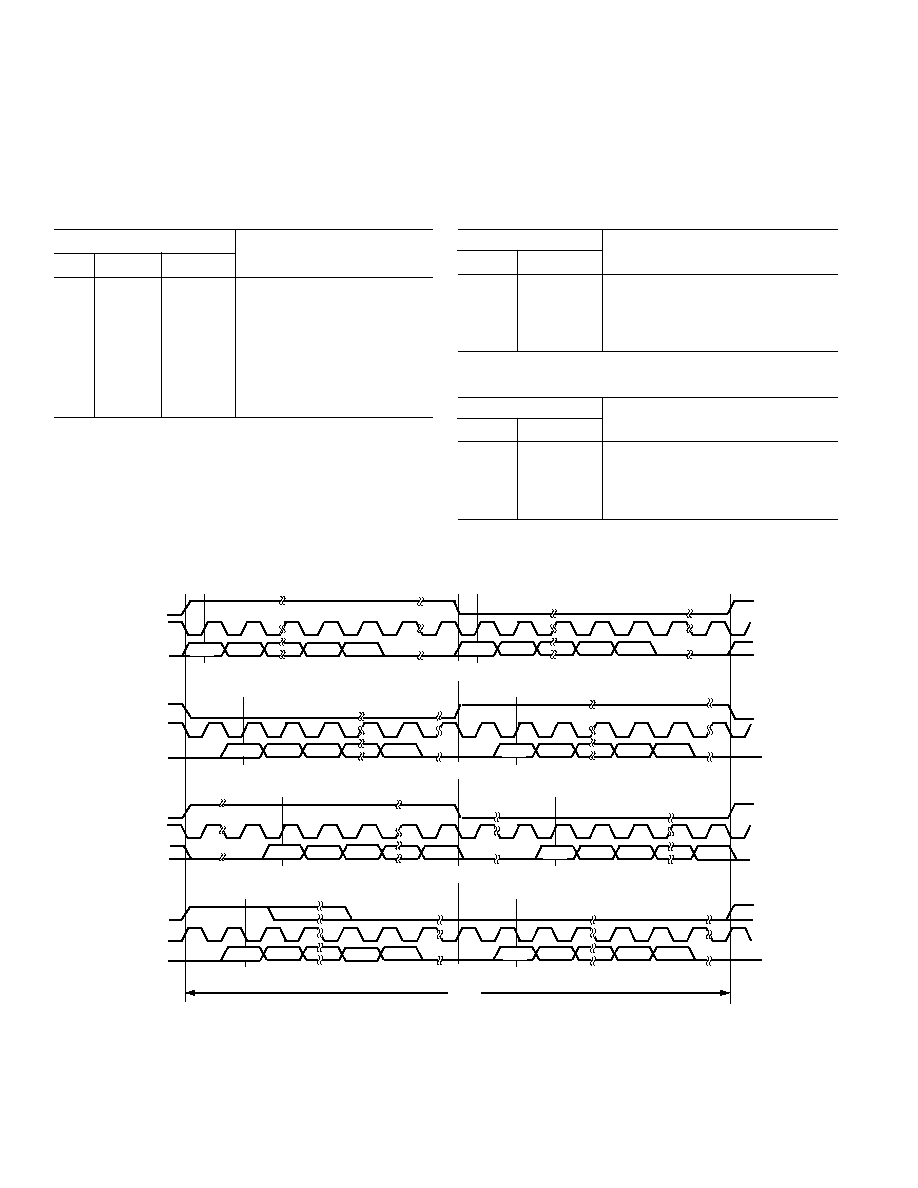
Table II. Serial Data Output Port Mode
SMODE_OUT_[0:2]
1
0
Interface Format
0
0
Left Justified (LJ)
0
1
I
2
S
1
0
TDM Mode
1
1
Right Justified (RJ)
Table III. Word Width
WLNGTH_OUT_[0:1]
1
0
Word Width
0
0
24 Bits
0
1
20 Bits
1
0
18 Bits
1
1
16 Bits
The following timing diagrams show the serial mode formats.
MSB
1/
f
s
TDM MODE ≠ 16 BITS TO 24 BITS PER CHANNEL
LEFT CHANNEL
RIGHT CHANNEL
LEFT CHANNEL
LEFT CHANNEL
RIGHT CHANNEL
RIGHT CHANNEL
MSB
LSB
LSB
LSB
LSB
LSB
LSB
MSB
LSB
MSB
LSB
LRCLK
SCLK
SDATA
LRCLK
SCLK
SDATA
LRCLK
SCLK
SDATA
LRCLK
SCLK
SDATA
NOTES
1. LRCLK NORMALLY OPERATES AT ASSOCIATIVE INPUT OR OUTPUT SAMPLE FREQUENCY (
f
s
)
2. SCLK FREQUENCY IS NORMALLY 64 LRCLK EXCEPT FOR TDM MODE, WHICH IS N
64
f
s
,
WHERE N = NUMBER OF STEREO CHANNELS IN THE TDM CHAIN. IN MASTER MODE, N = 4
MSB
MSB
MSB
MSB
MSB
MSB
MSB
I
2
S MODE ≠ 16 BITS TO 24 BITS PER CHANNEL
RIGHT-JUSTIFIED MODE ≠ SELECT NUMBER OF BITS PER CHANNEL
LEFT-JUSTIFIED MODE ≠ 16 BITS TO 24 BITS PER CHANNEL
Figure 10. Input/Output Serial Data Formats
Interface Format
REV. B
AD1895
≠21≠
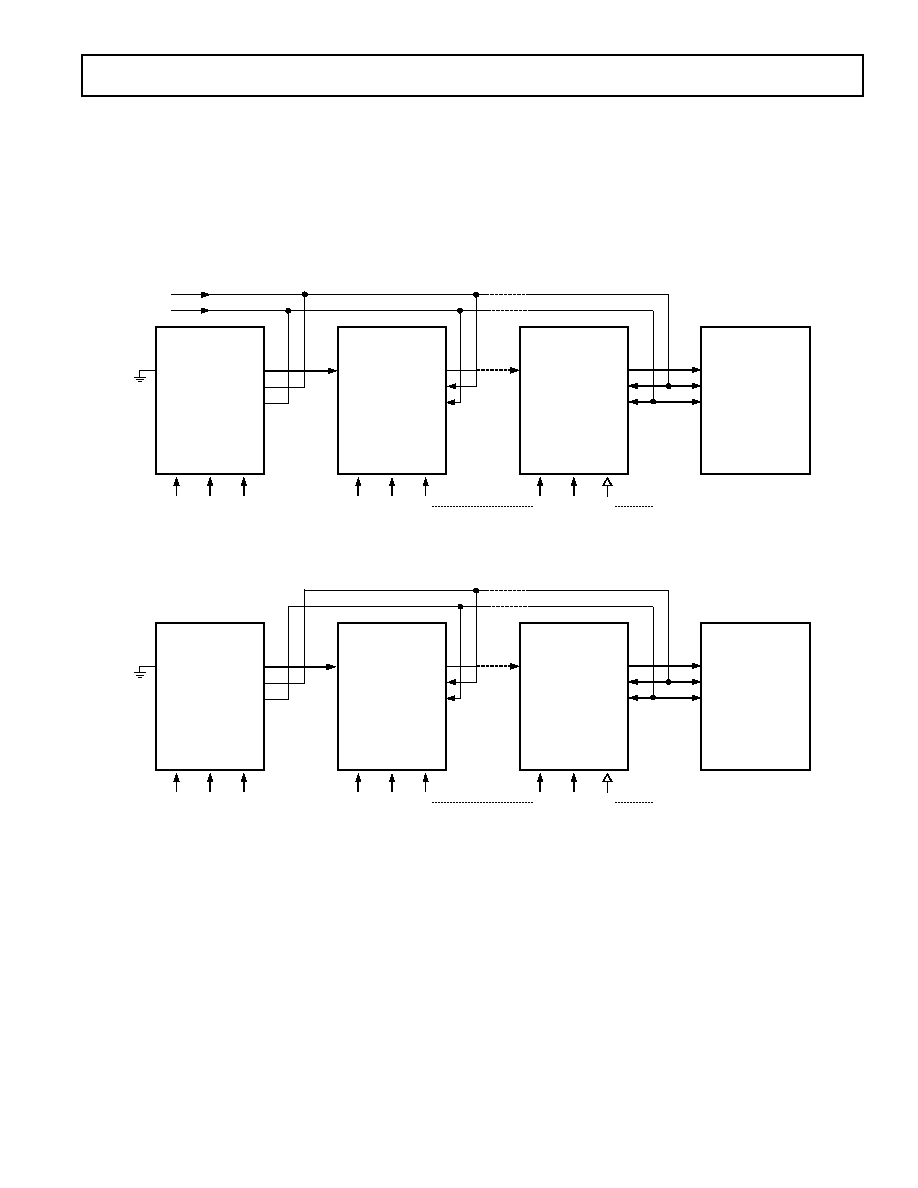
TDM MODE APPLICATION
In TDM Mode, several AD1895s can be daisy-chained together
and connected to the serial input port of a SHARC
Æ
DSP. The
AD1895 contains a 64-bit parallel load shift register. When the
LRCLK_O pulse arrives, each AD1895 parallel loads its left and
right data into the 64-bit shift register. The input to the shift
register is connected to TDM_IN, while the output is connected
to SDATA_O. By connecting the SDATA_O to the TDM_IN
of the next AD1895, a large shift register is created and is
clocked by SCLK_O.
The number of AD1895s that can be daisy-chained together is
limited by the maximum frequency of SCLK_O, which is about
25 MHz. For example, if the output sample rate, f
S
, is 48 kHz,
up to eight AD1895s could be connected since 512
◊ f
S
is less
than 25 MHz. In Master/TDM Mode, the number of AD1895s
that can be daisy-chained is fixed to four.
SHARC is a registered trademark of Analog Devices, Inc.
AD1895
TDM_IN
SDATA_O
LRCLK_O
M1
M2 M0
0
0 0
SCLK_O
SHARC
DSP
DR0
RFS0
RCLK0
SLAVE-2 SLAVE-n
STANDARD MODE
AD1895
TDM_IN
SDATA_O
LRCLK_O
M1
M2 M0
0
0 0
SCLK_O
AD1895
TDM_IN
SDATA_O
LRCLK_O
M1
M2 M0
SCLK_O
0
0 0
SCLK
LRCLK
SLAVE-1
Figure 11. Daisy-Chain Configuration for TDM Mode (All AD1895s Being Clock-Slaves)
AD1895
TDM_IN
SDATA_O
LRCLK_O
CLOCK-MASTER
M1
M2 M0
1
0 1
SCLK_O
SHARC
DSP
DR0
RFS0
RCLK0
SLAVE-1
SLAVE-n
STANDARD MODE
AD1895
TDM_IN
SDATA_O
LRCLK_O
M1
M2 M0
0
0 0
SCLK_O
AD1895
TDM_IN
SDATA_O
LRCLK_O
M1
M2 M0
SCLK_O
0
0 0
Figure 12. Daisy-Chain Configuration for TDM Mode (First AD1895 Being Clock-Master)

REV. B
AD1895
≠22≠
Serial Data Port Master Clock Modes
Either of the AD1895 serial ports can be configured as a
master serial data port. However, only one serial port can be
a master, while the other has to be a slave. In Master Mode, the
AD1895 requires a 256
◊ f
S
, 512 f
S
, or 768
◊ f
S
master clock
(MCLK_IN). For a maximum master clock frequency of 30 MHz,
the maximum sample rate is limited to 96 kHz. In Slave Mode,
sample rates up to 192 kHz can be handled.
When either of the serial ports is operated in Master Mode, the
master clock is divided down to derive the associated left/right
subframe clock (LRCLK) and serial bit clock (SCLK). The master
clock frequency can be selected for 256, 512, or 768 times the
input or output sample rate. Both the input and output serial
ports will support Master Mode LRCLK and SCLK generation
for all serial modes, left justified, I
2
S, right justified, and TDM
for the output serial port.
Table IV. Serial Data Port Clock Modes
MMODE_0/
MMODE_1/
MMODE_2
2
1
0
Interface Format
0
0
0
Both Serial Ports Are in Slave Mode
0
0
1
Output Serial Port Is Master with 768
◊ f
S_OUT
0
1
0
Output Serial Port Is Master with 512
◊ f
S_OUT
0
1
1
Output Serial Port Is Master with 256
◊ f
S_OUT
1
0
0
Undefined
1
0
1
Input Serial Port Is Master with 768
◊ f
S_IN
1
1
0
Input Serial Port Is Master with 512
◊ f
S_IN
1
1
1
Input Serial Port Is Master with 256
◊ f
S_IN
Bypass Mode
When the BYPASS pin is asserted high, the input data bypasses
the sample rate converter and is sent directly to the serial output
port. Dithering of the output data when the word length is set
to less than 24 bits is disabled. This mode is ideal when the
input and output sample rates are the same and LRCLK_I and
LRCLK_O are synchronous with respect to each other. This
mode can also be used for passing through nonaudio data,
since no processing is performed on the input data in this mode.

REV. B
AD1895
≠23≠
OUTLINE DIMENSIONS
28-Lead Shrink Small Outline Package [SSOP]
(RS-28)
Dimensions shown in millimeters
0.25
0.09
0.95
0.75
0.55
8
4
0
0.05
MIN
1.85
1.75
1.65
2.00 MAX
0.38
0.22
SEATING
PLANE
0.65
BSC
0.10
COPLANARITY
28
15
14
1
10.50
10.20
9.90
PIN 1
5.60
5.30
5.00
8.20
7.80
7.40
COMPLIANT TO JEDEC STANDARDS MO-150AH

REV. B
≠24≠
C00758≠0≠9/02(B)
PRINTED IN U.S.A.
AD1895
Revision History
Location
Page
9/02--Data Sheet changed from REV. A to REV. B.
Changes to SPECIFICATIONS (Digital Performance) . . . . . . . . . . . . . . . . . . . . . . . . . . . . . . . . . . . . . . . . . . . . . . . . . . . . . . . . . . 2
Changes to SPECIFICATIONS (Digital Timing) . . . . . . . . . . . . . . . . . . . . . . . . . . . . . . . . . . . . . . . . . . . . . . . . . . . . . . . . . . . . . . . 3
Changes to ORDERING GUIDE . . . . . . . . . . . . . . . . . . . . . . . . . . . . . . . . . . . . . . . . . . . . . . . . . . . . . . . . . . . . . . . . . . . . . . . . . . . 5
Replaced TPCs 1≠52 . . . . . . . . . . . . . . . . . . . . . . . . . . . . . . . . . . . . . . . . . . . . . . . . . . . . . . . . . . . . . . . . . . . . . . . . . . . . . . . . . . . . .7
Additions to
RESET and Power-Down section . . . . . . . . . . . . . . . . . . . . . . . . . . . . . . . . . . . . . . . . . . . . . . . . . . . . . . . . . . . . . . . . 19
Changes to Figures 9a and 9b . . . . . . . . . . . . . . . . . . . . . . . . . . . . . . . . . . . . . . . . . . . . . . . . . . . . . . . . . . . . . . . . . . . . . . . . . . . . . 19
Additions to Serial Data Ports≠≠Data Format section . . . . . . . . . . . . . . . . . . . . . . . . . . . . . . . . . . . . . . . . . . . . . . . . . . . . . . . . . . . 20
Updated OUTLINE DIMENSIONS . . . . . . . . . . . . . . . . . . . . . . . . . . . . . . . . . . . . . . . . . . . . . . . . . . . . . . . . . . . . . . . . . . . . . . . 23