
AC '97 SoundMAX CODEC
AD1986
Rev. 0
Information furnished by Analog Devices is believed to be accurate and reliable.
However, no responsibility is assumed by Analog Devices for its use, nor for any
infringements of patents or other rights of third parties that may result from its use.
Specifications subject to change without notice. No license is granted by implication
or otherwise under any patent or patent rights of Analog Devices. Trademarks and
registered trademarks are the property of their respective owners.
One Technology Way, P.O. Box 9106, Norwood, MA 02062-9106, U.S.A.
Tel: 781.329.4700
www.analog.com
Fax: 781.326.8703
© 2004 Analog Devices, Inc. All rights reserved.
FEATURES
AC `97 2.3 COMPLIANT FEATURES
6 DAC channels for 5.1 surround
S/PDIF output
Integrated headphone amplifiers
Variable rate audio
Double rate audio (F
s
= 96 kHz)
Greater than 90 dB dynamic range
20-bit resolution on all DACs
20-bit resolution on all ADCs
Line-level mono phone input
High quality CD input
Selectable MIC input w/preamp
AUX and line-in stereo inputs
External amplifier power down (EAPD)
Power management modes
Jack sensing and device identification
48-pin LQFP package
ENHANCED FEATURES
Integrated parametric equalizer
Stereo microphone with up to 30 dB gain boost
Integrated PLL for system clocking
Variable sample rate: 7 kHz to 96 kHz
7 kHz to 48 kHz in 1 Hz increments
96 kHz for double rate audio
Jack sense with auto topology switching
Jack presence detection on up to 8 jacks
Three software-controlled VREF_OUT signals
Software-enabled outputs for jack sharing
Auto-down mix and channel spreading
Microphone-to-mono output
Stereo microphone pass-through to mixer
Built-in microphone/center/LFE/line-in sharing
Built-in SURROUND/LINE_IN sharing
Center/LFE line swapping
Microphone swapping
Reduced support component count
General purpose digital output pin (GPO)
Separate LINE_OUT and HP_OUT pins
Headphone drivers on LINE_OUT and HP_OUT pins
Independent headphone/LINE_OUT operation

AD1986
Rev. 0 | Page 2 of 52
TABLE OF CONTENTS
Functional Block Diagram .............................................................. 4
Specifications..................................................................................... 5
AC '97 Timing Parameters .......................................................... 9
Absolute Maximum Ratings.......................................................... 12
Environmental Conditions........................................................ 12
ESD Caution................................................................................ 12
Pin Configuration And Function Description ........................... 13
AC '97 Registers .............................................................................. 15
Register Details ............................................................................... 17
Reset (Register 0x00).................................................................. 17
Master Volume (Register 0x02) ................................................ 17
Headphone Volume (Register 0x04)........................................ 18
Mono Volume (Register 0x06).................................................. 18
PC Beep (Register 0x0A)........................................................... 19
Phone Volume (Register 0x0C) ................................................ 19
Microphone Volume (Register 0x0E) ...................................... 20
Line In Volume (Register 0x10)................................................ 21
CD Volume (Register 0x12) ...................................................... 21
AUX Volume (Register 0x16) ................................................... 22
Front DAC Volume (Register 0x18)......................................... 22
ADC Select (Register 0x1A)...................................................... 23
ADC Volume (Register 0x1C) .................................................. 24
General-Purpose (Register 0x20)............................................. 25
Audio Int and Paging (Register 0x24) ..................................... 25
Power-Down Ctrl/Stat (Register 0x26).................................... 26
Ext'd Audio ID (Register 0x28)................................................. 27
Ext'd Audio Stat/Ctrl (Register 0x2A)...................................... 28
Front DAC PCM Rate (Register 0x2C) ................................... 29
Surround DAC PCM Rate (Register 0x2E) ............................ 30
C/LFE DAC PCM Rate (Register 0x30) .................................. 30
ADC PCM Rate (Register 0x32) .............................................. 30
C/LFE DAC Volume (Register 0x36)....................................... 31
Surround DAC Volume (Register 0x38) ................................. 31
SPDIF Control (Register 0x3A)................................................ 32
EQ Control Register (Register 0x60) ....................................... 33
EQ Data Register (Register 0x62) ............................................ 34
Misc Control Bits 2 (Register 0x70)......................................... 34
Jack Sense (Register 0x72)......................................................... 35
Serial Configuration (Register 0x74)....................................... 37
Misc Control Bits 1 (Register 0x76)......................................... 39
Advanced Jack Sense (Register 0x78) ...................................... 40
Misc Control Bits 3 (Register 0x7A)........................................ 41
Vendor ID Registers (Register 0x7C to 0x7E) ........................ 42
CODEC Class/Revision Register (Register 0x60).................. 42
PCI Subsystem Vendor ID Register (Register 0x62, Page 01)
....................................................................................................... 43
PCI Subsystem Device ID Register (Register 0x64, Page 01)43
Function Select Register (Register 0x66, Page 01)................. 43
Information and I/O Register (Register 0x68, Page 01)........ 44
Sense Register (Register 0x6A, Page 01) ................................. 46
Jack Presence Detection................................................................. 48
Audio Jack Styles (NC/NO) ...................................................... 48
Microphone Selection/Mixing...................................................... 49
Outline Dimensions ....................................................................... 50
Ordering Guide .......................................................................... 50
REVISION HISTORY
10/04--Initial Version: Revision 0

AD1986
Rev. 0 | Page 3 of 52
NOTES
REDUCED SUPPORT COMPONENTS
The AD1986's many improvements reduce external support
components for particular applications.
∑
Multiple Microphone Sourcing:
The MIC_1/2, LINE_IN
and C/LFE pins may all be selected as sources for
microphone input (boost amplifier).
∑
Multiple VREF_OUT Pins:
Each microphone-capable pin
group (MIC_1/2, LINE_IN and C/LFE) has separate,
software controllable VREF_OUT pins, reducing the need
for external biasing components.
∑
Internal Microphone Mixing:
Any combination of the
MIC_1/2, LINE_IN and C/LFE pins may be summed to
produce the microphone input. This removes the need for
external mixing components in those applications that
externally mixed microphone sources.
∑
Advanced Jack Presence Detection:
Using two CODEC
pins, eight resistors and isolated switch jacks, the AD1986
can detect jack insertion on eight separate jacks. Previous
CODECs would have required 8 CODEC pins and
16 resistors.
∑
Internal Microphone/Line In/C/LFE Sharing:
On systems
that share the microphone with the C/LFE jack there are
no external components required. The micro-phone
selector can select the LINE_IN pins in those cases where
the microphone and line input devices are swapped.
∑
Internal Line In/Microphone/Surround Sharing:
On
systems that share the line in with the surround jack there
are no external components required.
∑
Dual Headphone Amplifiers:
The AD1986 can drive
headphones out of the HP_OUT or LINE_OUT pins.

AD1986
Rev. 0 | Page 4 of 52
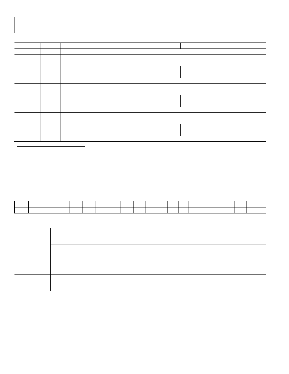
FUNCTIONAL BLOCK DIAGRAM
04785-0-003
DAC
SLOT
LOGIC
ADC
SLOT
LOGIC
AC '97 I
N
TE
RFACE
V
2
.
3
E
Q
COE
F
S
T
ORAGE
AC '97
CONTROL
REGISTERS
GPIO
EAPD
ANALOG M
I
X
I
NG CONTROL
JACK S
E
N
S
E
PLL
RESET
SYNC
BITCLK
SDATA_OUT
SDATA_IN
JACK_SENSE_A
JACK_SENSE_B
EAPD
GPO
VREF_OUT
(MIC1/2)
VREF_OUT
(C/LFE)
VREF_OUT
(LINE_IN)
VREF_FILT
20-BIT
20-BIT
-
ADC
CODEC CORE
24-BIT
-
DAC
24-BIT
-
DAC
24-BIT
-
DAC
24-BIT
-
DAC
EQ
24-BIT
-
DAC
EQ
24-BIT
-
DAC
-
ADC
M
G = GAIN
A = ATTENUATION
M = MUTE
Z = HI-Z
M
G
M
Z
G
M
GA
M
GA
M
GA
M
GA
M
GA
M
GA
M
A
M
GA
M
GA
M
GA
M
M
M
GA
M
GA
M
GA
M
GA
M
GA
M
GA
M
M
M
PHONE_IN
CD_L
CD_GND
CD_R
AUX_L
AUX_R
LINE_IN_L
CD
DIFF AMP
LINE
IN
SELECT
MICROPHONE
SELECTOR/
MIXING AND
GAIN BLOCK
LINE_IN_R
PCBEEP_IN
SPR
D
MZ
A
LFE_OUT
SPR
D
MZ
A
CENTER_OUT
SOSEL
MZ
A
SURR_OUT_L
SOSEL
MZ
A
SURR_OUT_R
LINE_OUT_L
M
A
MONO_OUT
LINE_OUT_R
M
A
HP_OUT_L
M
A
HP_OUT_R
HP
HP
MIX
H
PSEL
H
PSEL
M
A
M
A
HP
HP
LOSEL
LOSEL
G
Z
G
Z
G
VOLTAGE
REFERENCE
AD1986
AC97CK
SPDIF_OUT
SPDIF TX
RE
CORD
SELEC
TOR
PC BEEP
GENERATOR
MIC_1
MIC_2
Figure 1.

AD1986
Rev. 0 | Page 5 of 52
SPECIFICATIONS
Test conditions, unless otherwise noted.
Table 1.
Parameter Typ
Unit
Temperature 25
∞C
Digital Supply (DV
DD
) 3.3
±10%
V
Analog Supply (AV
DD
) 5.0
±10%
V
Sample Rate (F
S
) 48
kHz
Input Signal
1,008
Hz
Analog Output Pass Band
20 Hz≠20 kHz
V
IH
2.0 V
V
IL
0.8 V
V
IH
2.4 V
V
IL
0.6 V
DAC Test Conditions
Calibrated
Output -3 dB Relative to Full Scale
10 k Output Load: Line (Surround), Mono, Center, and LFE
32 Output Load: Headphone
ADC Test Conditions
Calibrated
0 dB PGA Gain
Input -3.0 dB Relative to Full Scale
Table 2. Analog Input
Input Voltage
Min
Typ
Max
Unit
MIC_1/2, LINE_IN, CD, AUX, PHONE_IN (No Preamp)
1
VRMS
1
C/LFE and SURROUND (When Used as Inputs)
2.83
V p-p
MIC_1/2, LINE_IN, C/LFE With 30 dB Preamp
0.032
VRMS
0.089
V
p-p
MIC_1/2, LINE_IN, C/LFE With 20 dB Preamp
0.1
VRMS
0.283
V
p-p
MIC_1/2, LINE_IN, C/LFE With 10 dB Preamp
0.316
VRMS
0.894
V
p-p
Input Impedance
2
20
k
Input Capacitance
2
5
7.5
pF
1
RMS values assume sine wave input.
2
Guaranteed by design, not production tested.
Table 3. Master Volume
Parameter
Min Typ Max Unit
Step Size (LINE_OUT, HP Out, Mono Out, SURROUND, CENTER, LFE)
-1.5
dB
Output Attenuation Range (0 dB to ≠46.5 dB)
-6.5
dB
Mute Attenuation of 0 dB Fundamental
2
-80
dB
Table 4. Programmable Gain Amplifier--ADC
Parameter
Min
Typ
Max
Unit
Step Size
1.5
dB
PGA Gain Range Span (0 dB to 22.5 dB)
22.5
dB

AD1986
Rev. 0 | Page 6 of 52
Table 5. Analog Mixer--Input Gain/Amplifiers/Attenuators
Parameter
Min Typ Max Unit
Signal-to-Noise Ratio (SNR)
CD to LINE_OUT
90
dB
LINE, AUX, PHONE to LINE_OUT
1
88
dB
MIC_1 or MIC_2 to LINE_OUT
1
80
dB
Step Size: All Mixer Inputs (Except PC Beep)
-1.5
dB
Step Size: PC Beep
-3.0
dB
Input Gain/Attenuation Range: All Mixer Inputs (+12 dB to -34.5 dB)
-46.5
dB
1
Guaranteed by design, not production tested.
Table 6. Digital Decimation and Interpolation Filters
1
Parameter
Min Typ Max Unit
Pass Band
0
0.4 ◊ F
S
Hz
Pass Band Ripple
±0.09
dB
Transition Band
0.4 ◊ F
S
0.6 ◊ F
S
Hz
Stop Band
0.6 ◊ F
S
Hz
Stop Band Rejection
-74
dB
Group Delay
16/F
S
S
Group Delay Variation Over Pass Band
0
µs
Table 7. Analog-to-Digital Converters
Parameter
Min Typ Max Unit
Resolution
20
Bits
Total Harmonic Distortion (THD)
-95
dB
Dynamic Range (-60 dB Input, THD + N referenced to Full Scale, A-Weighted)
-85
dB
Line Inputs (Input L, Ground R, Read R; Input R, Ground L, Read L)
-80
dB
LINE_IN to Other Inputs
-100
-80
dB
Gain Error (Full-Scale Span Relative to Nominal Input Voltage)
±10
%
Interchannel Gain Mismatch (Difference of Gain Errors)
±0.5
dB
ADC Offset Error
±5
mV

AD1986
Rev. 0 | Page 7 of 52
Table 8. Digital-to-Analog Converters
Parameter
Min Typ Max Unit
Resolution
24
Bits
Total Harmonic Distortion (LINE_OUT Drive)
-92
dB
Total Harmonic Distortion HP_OUT
-75
dB
Dynamic Range (-60 dB Input, THD + N referenced to Full Scale, A-Weighted)
91
dB
Gain Error (Full-Scale Span Relative to Nominal Input Voltage)
±10
%
Interchannel Gain Mismatch (Difference of Gain Errors)
±0.7
dB
DAC Crosstalk
1
(Input L, Zero R, Read R_OUT; Input R, Zero L, Read L_OUT)
-80
dB
1
Guaranteed by design, not production tested.
Table 9. Analog Output
Parameter
Min Typ
Max Unit
FULL-SCALE OUTPUT VOLTAGE: SURROUND, CENTER/LFE, MONO_OUT
1
VRMS
2.83
V
p-p
Output Impedance
1
300
External Load Impedance
1
10
k
Output Capacitance
1
15
pF
External Load Capacitance
1,000
pF
FULL-SCALE OUTPUT VOLTAGE: HP_OUT, LINE_OUT
1
VRMS
2.83
V
p-p
Output Impedance
1
1
External Load Impedance
1
32
Output Capacitance
1
15
pF
External Load Capacitance
1
1,000
pF
VREF_FILT, A
VDD
= 5.0 V
2.050
2.250
2.450
V
A
VDD
= 3.3 V
1.125
V
VREF_OUT(MIC, C/LFE, LIN) (xVREF [2:0] = 001)
2.250
V
(xVREF [2:0] = 100, A
VDD
= 5.0 V)
3.700
V
(xVREF [2:0] = 100, A
VDD
= 3.3 V)
2.250
V
(xVREF [2:0] = 010)
0.0
V
Current Drive
5
mA
Mute Click (Muted Output, Unmuted Midscale DAC Output)
±5
mV
Table 10. Static Digital Specifications--AC '97
Parameter
Min Typ
Max Unit
High Level Input Voltage (V
IH
), Digital Inputs
0.65 ◊ DV
DD
V
Low Level Input Voltage (V
IL
)
0.35 ◊ DV
DD
V
High Level Output Voltage (V
OH
), I
OH
= 2 mA
0.90 ◊ DV
DD
V
Low Level Output Voltage (V
OL
), I
OL
= 2 mA
0.10 ◊ DV
DD
V
Input Leakage Current
-10
10
µA
Output Leakage Current
-10
10
µA
Input/Output Pin Capacitance
7.5
pF

AD1986
Rev. 0 | Page 8 of 52
Table 11. Power Supply (Quiescent State)
Parameter
Min Typ
Max Unit
Power Supply Range--Analog (AV
DD
) ±10%
4.5
5.5
V
Power Supply Range--Digital (DV
DD
) ±10%
2.97
3.63
V
Power Dissipation--Analog (AV
DD
)/Digital (DV
DD
)
365/171.6
mW
Analog Supply Current--Analog (AV
DD
)
73
mA
Digital Supply Current--Digital (DV
DD
)
52
mA
Power Supply Rejection (100 mV p≠p Signal @ 1 kHz)
40
dB
Table 12. Power-Down States--AC '97 (Quiescent State)
Parameter
Set Bits
DV
DD
Typ AV
DD
Typ
Unit
ADC
PR0
53.0 45.7 mA
FRONT DAC
PR1
53.7
47.7
mA
CENTER DAC
PRI
62.0
53.2
mA
SURROUND DAC
PRJ
53.5
47.1
mA
LFE DAC
PRK
62.0
52.8
mA
ADC + ALL DACs
PR1, PR0, PRI, PRJ, PRK
27.0
14.5
mA
Mixer
PR2
36.6
53.2
mA
ADC + Mixer
PR2, PR0
27.6
45.7
mA
ALL DACs + Mixer
PR2, PR1, PRI, PRJ, PRK
12.6
33.0
mA
ADC + ALL DACs + Mixer
PR2, PR1, PR0, PRI, PRJ, PRK
2.4
14.5
mA
Standby
PR5, PR4, PR3, PR2, PR1(IJK), PR0
0.0
0.05
mA
Headphone
Standby
PR6
55.0 53.2 mA
LINE_OUT HP Standby
LOHPEN = 0
62.0
53.2
mA
Table 13. Clock Specifications--AC '97
1
Parameter
Min
Typ
Max
Unit
Input Clock Frequency (Reference Clock Mode)
14.31818
48.000
MHz
Recommended Clock Duty Cycle
40
50
60
%
1
Refer to AC '97, Revision 2.3 specifications for details of clock detection at startup. AD1986 CODEC clock source detection must follow AC '97, Revision 2.3 guidelines.
AD1986
Rev. 0 | Page 9 of 52
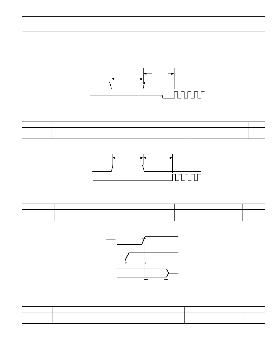
AC '97 TIMING PARAMETERS
Guaranteed over operating temperature range. Refer to the AC '97 specifications (Revision 2.3, Release 1.0) for further information. The
specification can be downloaded from http://developer.intel.com/ial.scalableplatforms/audio.
RESET
BIT_CLK
t
RST_LOW
t
RST2CLK
04785-0-005
Figure 2. Cold Reset Timing (CODEC is Supplying the BIT_CLK Signal)
Table 14.
Symbol
Parameter
Min
Typ
Max
Unit
t
RST_LOW
Recommended During Active (Low) RESET Signal
1.0
µS
t
RST2CLK
RESET Inactive (High) to BIT_CLK Active
162.8
400,000
nS
SYNC
BIT_CLK
t
SYNC_HIGH
t
SYNC2CLK
04785-0-006
Figure 3. Warm Reset Timing
Table 15.
Symbol
Parameter
Min
Typ
Max
Unit
t
SYNC_HIGH
Sync Active (High) Pulse Width
1.3
µS
t
SYNC2CLK
Sync Inactive to BITCLK Startup Delay
162.8
nS
t
SETUP2RST
t
OFF
Hi-Z
RESET
SDATA_OUT
SYNC
BIT_CLK, EAPD,
SPDIF_OUT,
SDATA_IN,
DIGITAL I/O
04785-0-007
re 4. ATE Test Mode
Table 16.
Symbol
Parameter
Min
Typ
Max
Unit
Figu
t
SETUP2RST
Setup to RESET Inactive (SYNC, SDATA_OUT)
15
nS
t
OFF
Rising Edge of RESET to Hi-Z Delay
25
nS
AD1986
Rev. 0 | Page 10 of 52
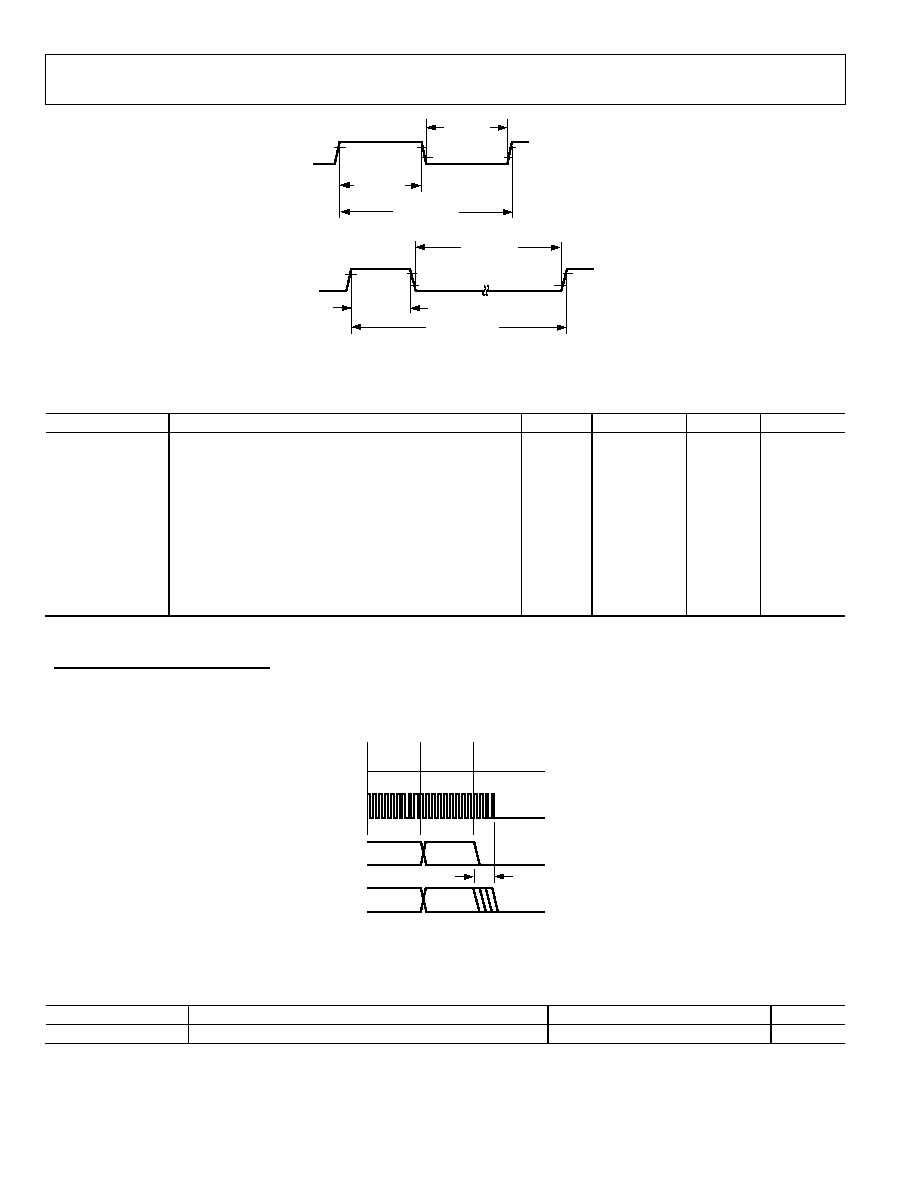
t
CLK_LOW
t
CLK_HIGH
t
CLK_PERIOD
t
SYNC_LOW
t
SYNC_PERIOD
t
SYNC_HIGH
BIT_CLK
SYNC
04785-0-008
Figure 5. Bit Clock and Sync Timing
Table 17.
Parameter
Min
Typ
Max
Units
Symbol
t
SYNC_HIGH
BITCLK High Pulse Width
40.5
41.7
nS
t
CLK_LOW
BITCLK Low Pulse Width
39.7
40.6
nS
t
CLK_PERIOD
BITCLK Period
81.4
nS
BIT_CLK Frequency
12.288
MHz
BIT_CLK Frequency Accuracy
±1.0
ppm
BIT_CLK
Jitter
1, 2
750
ps
t
SYNC_HIGH
Sync Active (High) Pulse Width
1.3
µS
t
SYNC_LOW
Sync Inactive (Low) Pulse Width
19.5
µS
t
SYNC_PERIOD
Sync Period
20.8
µS
Sync Frequency
48.0
kHz
1
by design, but not production tested.
r directly dependent on input clock jitter.
Guaranteed
2
Output jitte
BIT_CLK
SYNC
SDATA_IN
SDATA_OUT
BIT_CLK NOT TO SCALE
SLOT 1
SLOT 2
WRITE TO
03 26
DATA
PR4
t
S2_PDOWN
04785-0-009
Figure 6. Link Low Power Mode Timing
18.
Parameter
Min
Table
Symbol
Typ
Max
Units
t
S2_PDOWN
End
ATA_IN Low
of Slot 2 to BIT_CLK, SD
0
1.0
µS
AD1986
Rev. 0 | Page 11 of 52
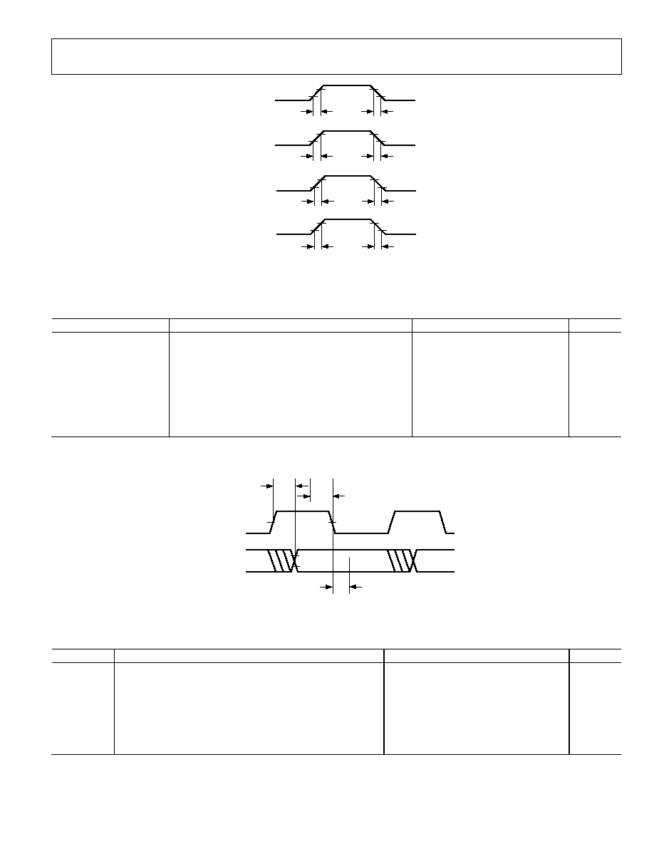
BIT_CLK
SYNC
SDATA_IN
SDATA_OUT
t
RISECLK
t
FALLCLK
t
RISESYNC
t
FALLSYNC
t
RISEDIN
t
FALLDIN
t
RISEDOUT
t
FALLDOUT
04785-0-010
Figure 7. Signal Rise and Fall Tim
ble 19.
mbol
Min
Typ
it
es
Ta
Sy
Parameter
Max
Un
t
RISECLK
4
6
BIT_CLK Rise Time
2
nS
t
FALLCLK
2
4
BIT_CLK Fall Time
6
nS
t
RISESYNC
SYNC Rise Time
2
4
6
nS
t
RISESYNC
SYNC Fall Time
2
4
6
nS
t
RISEDIN
SDATA_IN Rise Time
2
4
6
nS
t
RISEDIN
SDATA_IN Fall Time
2
4
6
nS
t
RISEDOUT
SDATA_OUT Rise Time
2
4
6
nS
t
RISEDOUT
SDATA_OUT Fall Time
2
4
6
nS
BIT_CLK
SDATA_OUT
SDATA_IN
SYNC
t
CO
t
SETUP
V
IH
V
IL
V
OH
V
OL
t
HOLD
04785-0-011
Figure 8. Link Low Power Mode Timing (Detail)
Table 20.
Symbol Parameter
Min
Typ Max
Unit
t
CO
Propagation Delay
25
nS
t
SETUP
Setup to Falling Edge of BIT_CLK
4
nS
t
HOLD
Hold from Falling Edge of BIT_CLK
3
nS
V
IH
Digital Signal High Level Input Voltage
0.65 DV
DD
V
V
IL
Digital Signal Low Level Input Voltage
0.35 DV
DD
V
V
OH
Digital Signal High Level Output Voltage
0.9 DV
DD
V
V
OL
Digital Signal Low Level Output Voltage
0.1 DV
DD
V

AD1986
Rev. 0 | Page 12 of 52
ABSOLUTE MAXIMUM RATINGS
Table 21.
Power Supply
Min
Max
Unit
Digital (DV
DD
)
-0.3 +3.6
V
Analog (AV
DD
)
-0.3
+6.0
V
Input Current (Except Supply Pins)
±10.0
mA
Analog Input Voltage (Signal Pins)
-0.3
AV
DD
+ 0.3
V
Digital Input Voltage (Signal Pins)
-0.3
DV
DD
+ 0.3
V
Ambient Temperature (Operating)
Commercial
Industrial
0
≠40
+70
+85
∞C
Storage Temperature
-65
+150
∞C
Stresses greater than those listed under Absolute Maximum
Ratings may cause permanent damage to the device. This is a
stress rating only and functional operation of the device at these
or any other conditions above those indicated in the operational
section of this specification is not implied. Exposure to absolute
maximum rating conditions for extended periods may affect
device reliability.
ENVIRONMENTAL CONDITIONS
Ambient Temperature Rating
T
AMB
= T
CASE
- (PD ◊
CA
)
T
CASE
= case temperature in ∞C
PD = power dissipation in W
CA
= thermal resistance (case-to-ambient)
JA
= thermal resistance (junction-to-ambient)
JC
= thermal resistance (junction-to-case)
Table 22. Thermal Resistance
Package
JA
JC
CA
LQFP 76.2∞C/W
17∞C/W
59.2∞C/W
ESD CAUTION
ESD (electrostatic discharge) sensitive device. Electrostatic charges as high as 4000 V readily accumulate on
the human body and test equipment and can discharge without detection. Although this product features
proprietary ESD protection circuitry, permanent damage may occur on devices subjected to high energy
electrostatic discharges. Therefore, proper ESD precautions are recommended to avoid performance
degradation or loss of functionality.

AD1986
Rev. 0 | Page 13 of 52
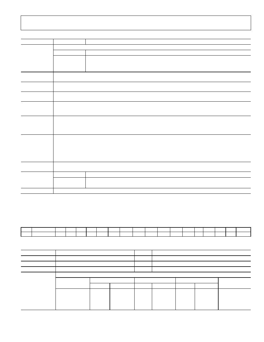
PIN CONFIGURATION AND FUNCTION DESCRIPTION
04785-0-001
PIN 1
IDENTIFIER
TOP VIEW
(Not to Scale)
AD1986
S/PD
IF_OU
T
EA
PD
AV
DD
LINE
_
O
UT_
R
AV
SS
LINE
_
O
UT_
L
AV
DD
HE
ADP
HONE
_
R
AV
SS
HE
ADP
HONE
_
L
AV
DD
MONO_
O
UT
PH
ON
E_IN
AUX
_
L
AUX
_
R
J
ACK_
S
E
N
S
E
_
A
J
ACK_
S
E
N
S
E
_
B
CD_
L
CD_
GND
CD_
R
MIC_
1
MIC_
2
LINE
_
I
N_
L
LINE
_
I
N_
R
DV
DD
AC97CK
GPO
DV
SS
SDATA_OUT
BIT_CLK
DV
SS
SDATA_IN
DV
DD
SYNC
RESET
PCBEEP
SURR_OUT_R
SURR_OUT_L
AV
DD
VREF_OUT (C/LFE)
LFE_OUT
CENTER_OUT
AV
SS
VREF_OUT (LINE_IN)
VREF_OUT (MIC_1/2)
VREF_FILT
AV
SS
AV
DD
48 47 46 45 44
39 38 37
43 42 41 40
1
2
3
4
5
6
7
8
9
10
11
12
13 14 15 16 17 18 19 20 21 22 23 24
36
35
34
33
32
31
30
29
28
27
26
25
Figure 9. Pin Configuration
Table 23. Pin Function Descriptions
Mnemonic Pin
Number
Input/Ouput Description
AC '97CK
2
I
External Clock In (14.31818 MHz).
SDATA_OUT
5
I
AC Link Serial Data Output. Input Stream.
BIT_CLK
6
O
AC Link Bit Clock. 12.288 MHz Serial Data Clock.
SDATA_IN
8
I/O
AC Link Serial Data Input. Output Stream.
SYNC
10
I
AC Link Frame Sync .
RESET
11
I
AC Link Reset. Master Hardware Reset.
Table 24. Digital Input/Output
Mnemonic
Pin
Number
Input/
Output Description
S/PDIF_OUT 48
O
S/PDIF Output.
EAPD
47
O
External Amplifier Power-Down Output.
GPO
3
O
General-Purpose Output pin. A digital signal that can be used to control external circuitry.
Table 25. Jack Sense
Mnemonic Pin
Number
Input/Ouput
Description
JACK_SENSE_A
16
I
JackSense 0≠3 Input
JACK_SENSE_B
17
I
Jack Sense 4≠7 Input

AD1986
Rev. 0 | Page 14 of 52
Table 26. Analog Input/Output
Mnemonic
Pin
Number
Input/
Ouput
Description
PCBEEP
12
I
Analog PC Beep Input. Routed to all output capable pins when RESET is asserted.
PHONE_IN
13
I
Monaural Line Level Input.
AUX_L
14
I
Auxiliary Left Channel Input.
AUX_R
15
I
Auxiliary Right Channel Input.
CD_L
18
I
CD-Audio-Left Channel.
CD_GND
19
I
CD-Audio-Analog-Ground-Reference (for Differential CD Input).
CD_R
20
I
CD-Audio-Right Channel.
MIC_1
21
I
Microphone 1 or Line-In-Left Input (See LISEL Bits in Register 0x76).
MIC_2
22
I
Microphone 2 or Line-In-Right Input (See LISEL Bits in Register 0x76).
LINE_IN_L
23
I
Line-In-Left Channel or Microphone 1 Input (See OMS Bits in Register 0x74).
LINE_IN_R
24
I
Line-In-Right Channel or Microphone 2 Input (See OMS Bits in Register 0x74).
CENTER_OUT
31
I/O
Center-Channel Output or Microphone 1 Input (See OMS Bits in Register 0x74).
LFE_OUT
32
I/O
Low-Frequency-Enhanced Output or Microphone 2 Input (See OMS Bits in Register 0x74).
HEADPHONE_L
39
O
Headphone-Out-Left Channel (See HPSEL Bits in Register 0x76).
HEADPHONE_R
41
O
Headphone-Out-Right Channel (See HPSEL Bits in Register 0x76).
LINE_OUT_L
43
O
Line-Out (Front)--Left Channel (See LOSEL Bit in Register 0x76) (HP Drive-Capable).
LINE_OUT_R
45
O
Line-Out (Front)--Right Channel (See LOSEL Bit in Register 0x76) (HP Drive-Capable).
MONO_OUT
37
O
Monaural Output to Telephony Subsystem Speakerphone.
SURR_OUT_L
35
I/O
Surround-Left Channel Output or Line-In-Left Input (See LISEL and SOSEL Bits in Register 0x76).
SURR_OUT_R
36
I/O
Surround-Right Channel Output or Line-In-Right Input (See LISEL and SOSEL Bits in
Register 0x76).
Table 27. Filter/Reference
Mnemonic
Pin
Number
Input/
Ouput
Description
VREF_FILT
27
O
Voltage Reference Filter.
VREF_OUT (MIC)
28
O
Programmable Voltage Reference Output (Intended for MIC Bias on the MIC_1/2 Channels).
VREF_OUT
(LINE_IN)
29
O
Programmable Voltage Reference Output (Intended for MIC Bias on the LINE_IN Channels).
VREF_OUT (C/LFE)
33
O
Programmable Voltage Reference Output (Intended for MIC Bias on the C/LFE Channels).
Table 28. Power and Ground
Mnemonic
Pin Number
Input/
Ouput
Description
DV
DD
1
Digital Supply Voltage (3.3 V).
9
DV
SS
4
Digital Supply Return (Ground).
7
AV
DD
25
Analog Supply Voltage (5.0 V or 3.3 V). AV
DD
supplies should be well filtered because supply
34
noise will degrade audio performance.
38 I
42
46
AV
SS
26
Analog Supply Return (Ground).
30
40
44

AD1986
Rev. 0 | Page 15 of 52
AC '97 REGISTERS
Table 29. Register Map
Reg
Name
D15 D14 D13 D12 D11 D10 D9 D8 D7 D6 D5 D4 D3 D2 D1 D0 Default
0x00
Reset
x
SE4 SE3 SE2 SE1 SE0 ID9 ID8 ID7 ID6 ID5 ID4 ID3 ID2 ID1 ID0 0x0290
0x02 Master
Volume
LM
x
x
LV4
LV3
LV2
LV1 LV0 RM x x
RV4 RV3 RV2 RV1 RV0 0x8080
0x04 Headphones Volume LM
x
x
LV4
LV3
LV2 LV1 LV0 RM x x
RV4 RV3 RV2 RV1 RV0 0x8080
0x06 Mono Volume
M
x
x
x
x
x
x
x
x
x
x
V4
V2
V2
V1
V0
0x8000
0x0A PC Beep
M
A/DS
x
F7
F6
F5
F4
F3
F2
F1
F0
V3
V2
V1
V0
x
0x8000
0x0C Phone Volume
M
x
x
x
x
x
x
x
x
x
x
V4
V3
V2
V1
V0
0x8008
0x0E Microphone Volume
LM
x
x
LV4
LV3
LV2
LV1
LV0
RM
M20 x
RV4
RV3
RV2
RV1
RV0
0x8888
0x10 Line In Volume
LM
x
x
LV4
LV3
LV2
LV1
LV0
RM
x
x
RV4
RV3
RV2
RV1
RV0
0x8888
0x12 CD Volume
LM
x
x
LV4
LV3
LV2
LV1
LV0
RM
x
x
RV4
RV3
RV2
RV1
RV0
0x8888
0x16 AUX Volume
LM
x
x
LV4
LV3
LV2
LV1
LV0
RM
x
x
RV4
RV3
RV2
RV1
RV0
0x8888
0x18 Front DAC Volume
LM
x
x
LV4
LV3
LV2
LV1
LV0
RM
x
x
RV4
RV3
RV2
RV1
RV0
0x8888
0x1A ADC Select
x
x
x
x
x
LS2
LS1
LS0
x
x
x
x
x
RS2
RS1
RS0
0x0000
0x1C ADC Volume
LM
x
x
x
LV3
LV2
LV1
LV0
RM
x
x
x
RV3
RV2
RV1
RV0
0x8080
0x20 General Purpose
x
x
x
x
DRSS1 DRSS0 MIX
MS
LPBK x
x
x
x
x
x
x
0x0000
0x24 Audio Int. and Paging I4
I3
I2
I1
I0
x
x
x
x
x
x
x
PG3
PG2
PG1
PG0
0xxx00
0x26 Power-Down Ctrl/Stat EAPD
PR6
PR5
PR4
PR3
PR2
PR1
PR0
x
x
x
x
REF
ANL
DAC
ADC
0x000x
0x28 Ext'd
Audio
ID
ID1
1
ID0
x
x
REV1
REV0
AMAP LDAC SDAC CDAC DSA1 DSA0
x
SPDF DRA
VRA
0x0BC7
0x2A Ext'd Audio Stat/Ctrl
x
x
PRK
PRJ
PRI
SPCV
x
LDAC SDAC CDAC SPSA1 SPSA0 x
SPDIF DRA
VRA
0x0xx0
0x2C Front DAC PCM Rate
R15
R14
R13
R12
R11
R10
R09
R08
R07
R06
R05
R04
R03
R02
R01
R00
0xBB80
0x2E Surr. DAC PCM Rate
R15
R14
R13
R12
R11
R10
R09
R08
R07
R06
R05
R04
R03
R02
R01
R00
0xBB80
0x30 C/LFE DAC PCM Rate R15
R14
R13
R12
R11
R10
R09
R08
R07
R06
R05
R04
R03
R02
R01
R00
0xBB80
0x32 ADC PCM Rate
R15
R14
R13
R12
R11
R10
R09
R08
R07
R06
R05
R04
R03
R02
R01
R00
0xBB80
0x36 C/LFE DAC Volume
LFEM
x
x
LFE4
LFE3
LFE2
LFE1
LFE0
CNTM x
x
CNT4
CNT3 CNT2 CNT1 CNT0 0x8888
0x38 Surround DAC Volume LM
x
x
LV4
LV3
LV2
LV1
LV0
RM
x
x
RV4
RV3
RV2
RV1
RV0
0x8888
0x3A SPDIF Control
V
VCFG
SPSR
x
L
CC6
CC5
CC4
CC3
CC2 CC1
CC0
PRE
COPY /AUDIO PRO
0x2000
0x60 EQ Control
EQM
x
x
x
x
x
x
x
SYM
CHS BCA5 BCA4
BCA3 BCA2 BCA1 BCA0 0x8080
0x62 EQ Data
CFD15
CFD14 CFD13 CFD12 CFD11 CFD10 CFD9
CFD8
CFD7 CFD6 CFD5 CFD4
CFD3 CFD2 CFD1 CFD0 0xxxxx
0x70 Misc. Control Bits 2
x
x
x
MVREF2 MVREF1 MVREF0 x
x
MMDIS x
JSMAP CVREF2 CVREF1 CVREF0 x
x
0x0000
0x72 Jack Sense
JS1 SPRD JS1 DMX JS0 DMX JS MT2 JS MT1 JS MT0 JS1 EQB JS0 EQB x
x
JS1 MD JS0 MD JS1 ST JS0 ST JS1 INT JS0 INT 0x0000
0x74 Serial
Configuration SLOT16 REGM2 REGM1 REGM0 REGM3 OMS2 OMS1 OMS0 SPOVR LBKS1 LBKS0 INTS
CSWP SPAL SPDZ SPLNK 0x1001
0x76 Misc. Control Bits 1
DACZ
AC97NC
2
MSPLT SODIS
3
CLDIS x
DMIX1 DMIX0 SPRD 2CMIC SOSEL SRU
LISEL1 LISEL0 MBG1 MBG0 0x6010
0x78 Advanced Jack Sense JS7ST
JS7INT JS6ST JS6INT JS5ST
JS5INT JS4ST
JS4INT JS4-7H
x
JS3MD
JS2MD JS3ST JS2ST JS3INT JS2INT 0xxxxx
0x7A Misc. Control Bits 3
JSINVB
HPSEL1 HPSEL0 LOSEL JSINVA LVREF2 LVREF1 LVREF0 x
x
x
LOHPEN GPO
MMIX x
x
0x0000
0x7C Vendor ID1
F7
F6
F5
F4
F3
F2
F1
F0
S7
S6
S5
S4
S3
S2
S1
S0
0x4144
0x7E Vendor ID2
T7
T6
T5
T4
T3
T2
T1
T0
REV7 REV6 REV5 REV4 REV3 REV2 REV1 REV0 0x5378
0x601 CODEC Class/Rev
x
x
x
CL4
CL3
CL2
CL1
CL0
RV7
RV6
RV5
RV4
RV3
RV2
RV1
RV0
0x0002
0x621 PCI SVID
PVI15
PVI14
PVI13
PVI12 PVI11 PVI10 PVI9
PVI8
PVI7
PVI6 PVI5
PVI4
PVI3
PVI2
PVI1
PVI0
0xFFFF
0x641 PCI SID
PI15
PI14
PI13
PI12
PI11
PI10
PI9
PI8
PI7
PI6
PI5
PI4
PI3
PI2
PI1
PI0
0xFFFF

AD1986
Rev. 0 | Page 16 of 52
Reg
Name
D15 D14 D13 D12 D11 D10 D9 D8 D7 D6 D5 D4 D3 D2 D1 D0 Default
0x661 Function Select
x
x
x
x
x
x
x
x
x
x
x
FC3
FC2
FC1
FC0
T/R
0x0000
0x681 Function Information G4
G3
G2
G1
G0
INV
DL4
DL3
DL2
DL1
DL0
IV
x
x
x
FIP
0xXxxx
0x6A1 Sense Register
ST2
ST1
ST0
S4
S3
S2
S1
S0
OR1
OR0 SR5
SR4
SR3
SR2
SR1
SR0
0xXxxx
1
CODEC is always master, ID bits are read-only 0 (zeros).
2
Bits for the AD198x are backwards-compatible only, AC97NC and MSPLT are read-only 1 (ones).
3
SODIS/SOSEL were LODIS/LOSEL in the AD1985. Most AD1985 configurations swapped LINE_OUT and SURROUND pins; these bits really operated as SO not LO.

Preliminary Technical Data
AD1986
Rev. 0 | Page 17 of 52
REGISTER DETAILS
RESET (REGISTER 0x00)
Writing any value to this register performs a register reset, which causes all registers to revert to their default values. The serial
configuration (0x74) register will not reset the SLOT16, REGM [2:0], SPOVR, SPAL, SPDZ, and SPLNK. These bits are reset on a hard,
hardware, or power-on reset. The REGM and serial configuration bits are only reset only by an external hardware reset.
The AC '97, Revision 2.3, Page 1 registers CODEC class/rev (0x601), PCI SVID (0x621), PCI SID (0x641), function information (0x681--
per supported function), and sense register ST [3:0] bits (0x6A1 D [15:13]--per supported function) are only reset on a power-on reset.
To satisfy the AC '97, Revision 2.3 requirements, these registers/bits are sticky across all software and hardware resets.
Reading this register returns the ID code of the part and a code for the type of 3D stereo enhancement.
Reg Name
D15
D14
D13
D12
D11
D10
D9 D8 D7 D6 D5 D4 D3 D2 D1 D0 Default
0x00 Reset x
SE4 SE3
SE2 SE1 SE0 ID9 ID8 ID7 ID6 ID5 ID4 ID3 ID2 ID1 ID0 0x0290
Table 30.
Register Function
The ID decodes the capabilities of the AD1986 based on the functions.
Bit Function
AD1986
ID
[9:0]
ID0
Dedicated MIC PCM In channel
0
ID1
Reserved (per AC '97, Revision 2.3)
0
ID2
Bass and treble control
0
ID3
Simulated stereo (mono to stereo)
0
ID4
Headphone out support
1
0x290
ID5
Loudness (bass boost) support
0
ID6
18-bit DAC resolution
0
ID7
20-bit DAC resolution
1
ID8
18-bit ADC resolution
0
ID [9:0] (RO)
(Identify
Capability)
ID9
20-bit ADC resolution
1
SE [4:0] (RO)
(Stereo
Enhancement)
The AD1986 does not provide hardware 3D stereo enhancement
(all bits are zero).
Default: 0x00
x Reserved.
Default: 0
MASTER VOLUME (REGISTER 0x02)
This register controls the LINE_OUT, SURROUND, and CENTER/LFE outputs' mute and volume controls in unison. Each volume sub-
register contains five bits, generating 32 volume steps of -1.5 dB each for a range of 0 dB to -46.5dB.
The headphone output (HP_OUT) mute and volume are controlled separately by the headphones volume register (0x04).The monaural
output (MONO_OUT) mute and volume is controlled separately by the mono volume register (0x06). To control the LINE_OUT,
SURROUND, and CENTER/LFE volumes separately use the front DAC volume register (0x18) for LINE_OUT; the surround DAC
Volume register (0x38) for SURROUND; and the C/LFE DAC volume register (0x36) for CENTER/LFE.
Reg Name
D15 D14 D13 D12 D11 D10 D9 D8 D7 D6 D5 D4 D3 D2 D1 D0 Default
0x02
Master
Volume
LM x
x
LV4 LV3 LV2 LV1 LV0 RM x x RV4 RV3 RV2 RV1 RV0 0x8080

AD1986
Preliminary Technical Data
Rev. 0 | Page 18 of 52
Table 31.
Register Function
Left/right volume controls the left/right channel output gains from 0 dB to ≠46.5 dB.
The least significant bit represents ≠1.5 dB.
L/RM L/RV
[4:0]
Function
Default
0
0 0000
0 dB
Default
0
0 1111
-22.5 dB attenuation
0
1 1111
-46.5 dB attenuation
L/RV [4:0]
(Left/Right
Volume)
1 x
xxxx
Muted
L/RM
(Left/right mute)
Mutes the left/right channels independently. Default:
muted
(0x1)
x Reserved.
Default: 0
HEADPHONE VOLUME (REGISTER 0x04)
This register controls the HP_OUT mute and volume controls. Each volume subregister contains five bits, generating 32 volume steps of
-1.5 dB each for a range of 0 dB to -46.5 dB.
Reg Name
D15 D14 D13 D12 D11 D10 D9 D8 D7 D6 D5 D4 D3 D2 D1 D0 Default
0x04
Headphones
Volume
LM x
x
LV4 LV3 LV2 LV1 LV0 RM x x RV4 RV3 RV2 RV1 RV0 0x8080
Table 32.
Register Function
Left/right volume controls the left/right channel output gains from 0 dB to ≠46.5 dB.
The least significant bit represents ≠1.5 dB.
L/RM L/RV
[4:0]
Function
Default
0
0 0000
0 dB
Default
0
0 1111
-22.5 dB attenuation
0
1 1111
-46.5 dB attenuation
L/RV [4:0]
(Left/Right
Volume)
1 x
xxxx
Muted
L/RM
(Left/Right Mute)
Mutes the left/right channels independently. Default:
muted
(0x1)
x Reserved.
Default: 0
MONO VOLUME (REGISTER 0x06)
This register controls the MONO_OUT mute and volume control. The volume register contains five bits, generating 32 volume steps of
-1.5 dB each for a range of 0 dB to -46.5 dB.
Reg Name
D15 D14 D13 D12 D11 D10 D9 D8 D7 D6 D5 D4 D3 D2 D1 D0 Default
0x06 Mono
Volume M x
x
x
x
x
x x x x x V4 V3 V2 V1 V0 0x8000
Table 33.
Register Function
V [4:0]
Volume controls the output gain from 0 dB to ≠46.5 dB. The least significant bit represents -1.5 dB.
(Volume)
M V
[4:0]
Function
Default
0
0 0000
0 dB
Default
0
0 1111
-22.5 dB attenuation
0
1 1111
-46.5 dB attenuation
1 x
xxxx
Muted
M (Mute)
Mutes the output. Default:
muted
(0x1)
x Reserved.
Default: 0

Preliminary Technical Data
AD1986
Rev. 0 | Page 19 of 52
PC BEEP (REGISTER 0x0A)
This controls the level of the Analog PC beep or the level and frequency of the Digital PC beep. The volume register contains four bits,
generating 16 volume steps of -3.0 dB each for a range of 0 dB to -45.0 dB. The tone frequency can be set between 47 Hz to 12,000 Hz or
disabled.
Per Intel's BIOS writer's guide, the PC beep signal should play via headphone out, line out, and mono out paths. BIOS algorithms should
unmute the PC beep register and the path to each output, and set the volume levels for playback.
When the AD1986 is in reset (the external RESET pin is low), the PCBEEP_IN pin is connected internally to all of the device output pins
(HEADPHONE L/R, LINE_OUT L/R, MONO_OUT, SURROUND L/R, and CENTER/LFE). There are no amplifiers or attenuators on
this path and the external circuitry connected to this pin should anticipate the drive requirements for the multiple output sources.
Headphones connected to output pins will substantially load the signal.
Reg Name D15 D14 D13 D12 D11 D10 D9 D8 D7 D6 D5 D4 D3 D2 D1 D0 Default
0x0A
PC
Beep
M A/DS
x
F7 F6 F5 F4 F3 F2 F1 F0 V3 V2 V1 V0 x 0x8000
Table 34.
Register Function
Controls the gain into the output mixer from 0 dB to -45.0 dB. The least significant bit represents -3.0 dB. The gain default
is 0 dB and muted.
M V3...V0
Function
Default
0 0000
0
dB
Default
0
1111
-45 dB attenuation
1 xxxx
Muted
V [3:0]
(Analog or
Digital
Volume)
The result of dividing the 48 kHz clock by four times this number, allowing tones from 47 Hz to 12 kHz. A value of 0x00
disables internal PC beep generation. The digitally-generated signal is close to a square wave and is not intended to be a
high quality signal.
F7...F0 Function
0000
Disabled
Default
0001
12,000 Hz tone
F [7:0]
(PC Beep
Frequency)
1111
47 Hz tone
A/DS
(PC Beep
Source)
Selects either the digital PC beep generator (= 0) or analog PCBEEP pin (= 1). When the
CODEC is in reset mode the analog PCBEEP pin is routed to the outputs via a high
impedance path. Once ot of reset, this bit must be programmed to a 1 to pass through any
signals on the analog PCBEEP pin. Designers may choose not to connect the analog PCBEEP
pin and use the digital PC beep generator solely.
Default: digitally-selected
(0x0)
M
(PC Beep
Mute)
When this bit is set to 1, the PC beep signal (analog or digital) is muted.
Default: muted (0x1)
x Reserved.
Default:
0
PHONE VOLUME (REGISTER 0x0C)
This register controls the PHONE_IN mute and gain to the analog mixer section. The volume register contains five bits, generating
32 volume steps of 1.5 dB each for a range of 12.0 dB to -34.5 dB. This does not control the record ADC gain (see Register 0x1C).
Reg Name
D15 D14 D13 D12 D11 D10 D9 D8 D7 D6 D5 D4 D3 D2 D1 D0 Default
0x0C
Phone
Volume
M x x
x x x x x x x x V4
V3
V2
V1
V0
0x8008

AD1986
Preliminary Technical Data
Rev. 0 | Page 20 of 52
Table 35.
Register
Function
Controls the gain of this input to the analog mixer from 12.0 dB to -34.5 dB. The least significant bit represents -1.5 dB.
MV [4:0]
Function
Default
0
0 0000
12 dB gain
0
0 1000
0 dB
Default
0 1
1111 -34.5 dB attenuation
V [4:0]
(Volume)
1 x
xxxx
Muted
M (Mute)
Mutes the input to the analog mixer.
Default: muted (0x1)
x Reserved.
Default: 0
MICROPHONE VOLUME (REGISTER 0x0E)
This register controls the MIC_1 (left) and MIC_2 (right) channels' gain, boost, and mute to the analog mixer section. The volume
register contains five bits, generating 32 volume steps of -1.5 dB each for a range of +12.0 dB to -34.5 dB. This does not control the
record ADC gain (see Register 0x1C).
In typical stereo microphone applications, the signal paths must be identical and should be set to the same gain, boost, and mute values.
With stereo controls, this input is capable of nonmicrophone sources by disabling the microphone boost (M20 Bit = 0).
Reg Name
D15 D14 D13 D12 D11 D10 D9 D8 D7 D6 D5 D4 D3 D2 D1 D0 Default
0x0E
Microphone
Volume
LM x x
LV4 LV3 LV2 LV1 LV0 RM M20 x RV4 RV3 RV2 RV1 RV0 0x8888
Table 36.
Register
Function
Controls the left/right channel gains of this input to the analog mixer from +12 dB to -34.5 dB. The least significant bit
represents -1.5 dB.
L/RM L/RV
[4:0]
Function
Default
0
0 0000
12 dB gain
0
0 1000
0 dB
Default
0
1 1111
-34.5 dB attenuation
L/RV [4:0]
(Left/Right
Volume)
1 x
xxxx
Mute
Enables additional gain to increase the microphone sensitivity. This controls the boost of both the MIC_1 and MIC_2 channels.
The nominal gain boost by default is 20 dB; however, MBG0 [1:0] bits (Register 0x76), allow changing the gain boost to 10 dB
or 30 dB if necessary.
M20
MGB0 [1:0]
Boost Gain
0
xx
0 dB gain
Default: disabled
1
00
20 dB gain
Default
1
01
10 dB gain
M20
(MIC_1/2
Gain
Boost)
1 x
xxxx
Mute
L/RM
(Left/Right
Mute)
Mutes the left/right channels independently. Default:
muted
(0x1)
x Reserved.
Default:
0
Preliminary Technical Data
AD1986
Rev. 0 | Page 21 of 52
LINE IN VOLUME (REGISTER 0x10)
This register controls the LINE_IN gain and mute to the analog mixer section. The volume register contains five bits, generating
32 volume steps of -1.5 dB each for a range of +12.0 dB to -34.5 dB. This does not control the record ADC gain (see Register 0x1C).
Reg Name
D15 D14 D13 D12 D11 D10 D9 D8 D7 D6 D5 D4 D3 D2 D1 D0 Default
0x10
Line In
Volume
LM x x
LV4 LV3 LV2 LV1 LV0 RM x x RV4 RV3 RV2 RV1 RV0 0x8888
Table 37.
Register Function
Controls the left/right channel gains of this input to the analog mixer from 12 dB to -34.5 dB. The least significant bit
represents -1.5 dB.
L/RM L/RV
[4:0]
Function
Default
0
0 0000
12 dB gain
0
0 1000
0 dB
Default
0
1 1111
-34.5 dB attenuation
L/RV [4:0]
(Left/Right
Volume)
1 x
xxxx
Muted
L/RM
(Left/Right
Mute)
Mutes the left/right channels independently. Default:
muted
(0x1)
x Reserved.
Default: 0
CD VOLUME (REGISTER 0x12)
This register controls the CD gain and mute to the analog mixer section. The volume register contains five bits, generating 32 volume
steps of -1.5 dB each for a range of +12.0 dB to -34.5 dB. This does not control the record ADC gain (see Register 0x1C).
Many operating systems will play CDs directly using the digital data from the CD tracks. This control will only affect CD audio playback
if it is enabled for analog and this input is connected to the CD player analog connection.
Reg Name
D15 D14 D13 D12 D11 D10 D9 D8 D7 D6 D5 D4 D3 D2 D1 D0 Default
0x12 CD
Volume LM x
x
LV4 LV3 LV2 LV1 LV0 RM x x RV4 RV3 RV2 RV1 RV0 0x8888
Table 38.
Register
Function
Controls the left/right channel gains of this input to the analog mixer from +12 dB to ≠34.5 dB. The least significant bit
represents ≠1.5 dB.
L/RM L/RV
[4:0]
Function
Default
0
0 0000
12 dB gain
0
0 1000
0 dB
Default
0 1
1111
-
34.5 dB attenuation
L/RV [4:0]
(Left/Right
Volume)
1 x
xxxx
Muted
L/RM
(Left/Right
Mute)
Mutes the left/right channels independently. Default:
muted
(0x1)
x Reserved.
Default: 0

AD1986
Preliminary Technical Data
Rev. 0 | Page 22 of 52
AUX VOLUME (REGISTER 0x16)
This register controls the AUX_IN gain and mute to the analog mixer section. The volume register contains five bits, generating
32 volume steps of -1.5 dB each for a range of +12.0 dB to -34.5 dB. This does not control the record ADC gain (see Register 0x1C).
Reg Name
D15 D14 D13 D12 D11 D10 D9 D8 D7 D6 D5 D4 D3 D2 D1 D0 Default
0x16
AUX
Volume
LM x x
LV4 LV3 LV2 LV1 LV0 RM x x RV4 RV3 RV2 RV1 RV0 0x8888
Table 39.
Register Function
Controls the left/right channel gains of this input to the analog mixer from +12 dB to -34.5 dB. The least significant bit
represents -1.5 dB.
L/RM L/RV
[4:0]
Function
Default
0
0 0000
12 dB gain
0
0 1000
0 dB
Default
0
1 1111
-34.5 dB attenuation
L/RV [4:0]
(Left/Right
Volume)
1 x
xxxx
Mute
L/RM
(Left/Right
Mute)
Mutes the left/right channels independently. Default:
muted
(0x1)
x Reserved.
Default: 0
FRONT DAC VOLUME (REGISTER 0x18)
This register controls the front DAC gain and mute to the analog mixer section. The volume register contains five bits, generating
32 volume steps of -1.5 dB each for a range of +12.0 dB to -34.5 dB.
Reg Name
D15 D14 D13 D12 D11 D10 D9 D8 D7 D6 D5 D4 D3 D2 D1 D0 Default
0x18
Front DAC
Volume
LM x x
LV4 LV3 LV2 LV1 LV0 RM x x RV4 RV3 RV2 RV1 RV0 0x8888
Table 40.
Register
Function
Controls the left/right channel gains of this input to the analog mixer from +12 dB to -34.5 dB. The least significant
bit represents -1.5 dB.
L/RM L/RV
[4:0] Function
Default
0
0 0000
+12 dB gain
0
0 1000
0 dB
Default
0
1 1111
-34.5 dB attenuation
L/RV [4:0]
(Left/Right Volume)
1 x
xxxx Mute
L/RM
(Left/Right Mute)
Mutes the left/right channels independently. Default:
muted
(0x1)
x Reserved.
Default: 0

Preliminary Technical Data
AD1986
Rev. 0 | Page 23 of 52
ADC SELECT (REGISTER 0x1A)
This register selects the record source for the ADC, independently for the right and left channels. The default value is 0x0000, which
corresponds to the MIC_1/2 input for both channels.
Reg Name D15 D14 D13 D12 D11 D10 D9 D8 D7 D6 D5 D4 D3 D2 D1 D0 Default
0x1A
ADC
Select
x x x
x x LS2
LS1
LS0
x x x x x RS2
RS1
RS0
0x0000
Table 41.
Register
LS [2:0]
Left Record Source
Function
000
MIC_1/2 selector left channel
Default
001 CD_IN
Left
010 Muted
011 AUX_IN
Left
100 LINE_IN
Left
101 Stereo
output
mix
Left
110
Mono output mix
Mono
LS [2:0]
(Left Record Select)
111 PHONE_IN
Mono
RS [2:0]
Right Record Source
000
MIC_1/2 selector left channel
Default
001 CD_IN
Right
010 Muted
011 AUX_IN
Right
100 LINE_IN
Right
101 Stereo
output
mix
Right
110
Mono output mix
Mono
RS [2:0]
(Right Record Select)
111 PHONE_IN
Mono
Table 42. Microphone Selector
OMS [2:0]
1
MMIX
2
2CMIC
3
MS
4
Left Channel
5
Right Channel
000 0
0 0
MIC_1
(default)
000 0
0 1
MIC_2
000 0
1 0
MIC_1
MIC_2
000 0
1 1
MIC_2
MIC_1
000
1
x
x
MIC_1 + MIC_2 (mixed)
001 0
0 0
LINE_IN
left
001
0 0 1
LINE_IN
right
001
0
1
0
LINE_IN left
LINE_IN right
001
0
1
1
LINE_IN right
LINE_IN left
001
1
x
x
Line in--left + right (mixed)
01x 0
0 0
CENTER
01x
0 0 1
LFE
01x
0 1 0
CENTER
LFE
01x
0 1 1
LFE
CENTER
01x
1
x
x
CENTER + LFE (mixed)
100
0
0
0
MIC_1 + CENTER (mixed)
100
0
0
1
MIC_2 + LFE (mixed)
100
0
1
0
MIC_1 + CENTER (mixed)
MIC_2 + LFE (mixed)
100
0
1
1
MIC_2 + LFE (mixed)
MIC_1 + CENTER (mixed)
100
1
x
x
MIC_1 + MIC_2 + CENTER + LFE (mixed)
AD1986
Preliminary Technical Data
Rev. 0 | Page 24 of 52
OMS [2:0]
1
MMIX
2
2CMIC
3
MS
4
Left Channel
5
Right Channel
101
0
0
0
MIC_1 + LINE_IN left (mixed)
101
0
0
1
MIC_2 + LINE_IN right (mixed)
101
0
1
0
MIC_1 + LINE_IN left (mixed)
MIC_2 + LINE_IN right (mixed)
101
0
1
1
MIC_2 + LINE_IN right (mixed)
MIC_1 + LINE_IN left (mixed)
101
1
x
x
MIC_1 + MIC_2 + LINE_IN left + LINE right (mixed)
110
0
0
0
LINE_IN left + CENTER (mixed)
110
0
0
1
LINE_IN right + LFE (mixed)
110
0
1
0
LINE_IN left + CENTER (mixed)
LINE_IN right + LFE (mixed)
110
0
1
1
LINE_IN right + LFE (mixed)
LINE_IN left + CENTER (mixed)
110
1
x
x
LINE_IN left + LINE_IN right + CENTER + LFE (mixed)
111
0
0
0
MIC_1 + LINE_IN left + CENTER (mixed)
111
0
0
1
MIC_2 + LINE_IN right + LFE (mixed)
111
0
1
0
MIC_1 + LINE_IN left + CENTER (mixed)
MIC_2 + LINE_IN right + LFE (mixed)
111
0
1
1
MIC_2 + LINE_IN right + LFE (mixed)
MIC_1 + LINE_IN left + CENTER (mixed)
111
1
x
x
MIC_1 + MIC_2 + LINE_IN left + LINE_IN right + CENTER + LFE (mixed)
1
To select the alternate pins as a microphone source, see the OMS [2:0] bit (Register 0x74).
2
To mix the left/right MIC channels see MMIX bit (Register 0x7A).
3
For dual MIC recording see 2CMIC bit (Register 0x76) to enable simultaneous recording into L/R channels.
4
To swap left/right MIC channels, see the MS bit (Register 0x20) for MIC_1/2 selection.
5
The MONO_OUT pin may be connected to the left channel of the microphone selector and is affected by these bits.
ADC VOLUME (REGISTER 0x1C)
This register controls the mute and gain of the ADC record path. The volume register contains four bits, generating 16 volume steps of
1.5 dB each for a range of 0 dB to 22.5 dB.
Reg Name
D15 D14 D13 D12 D11 D10 D9 D8 D7 D6 D5 D4 D3 D2 D1 D0 Default
0x1C ADC
Volume LM x
x
x
LV3 LV2 LV1 LV0 RM x x x RV3 RV2 RV1 RV0 0x8080
Table 43.
Register
Function
Controls the left/right channel gains of this input to the analog mixer from 0 dB to 22.5 dB The least significant bit
represents 1.5 dB.
L/RM L/RV
[3:0]
Function
Default
0 0000
0
dB
Default
0
1000
12.0 dB gain
0
1111
22.5 dB gain
L/RV [4:0]
(Left/Right
Volume)
1 xxxx
Muted
L/RM
(Left/Right Mute)
Mutes the left/right channels independently. Default:
muted
(0x1)
x Reserved.
Default: 0
Preliminary Technical Data
AD1986
Rev. 0 | Page 25 of 52
GENERAL-PURPOSE (REGISTER 0x20)
This register should be read before writing to generate a mask for only the bit(s) that need to be changed.
Reg Name
D15 D14 D13 D12 D11 D10 D9 D8 D7 D6 D5 D4 D3 D2 D1 D0 Default
0x20
General-
Purpose
x x x
x
DRSS1 DRSS0 MIX MS LPBK x x x x x x x 0x0000
Table 44.
Register Function
Default
LPBK
(Loop-
Back
Control)
This bit enables the digital internal loop back from the ADC to the front DAC. This feature is normally used for
testing and troubleshooting. See LBKS bit in Register 0x74 for changing the loop back path to use the
SURROUND or CENTER/LFE DACs.
Default:
disabled
(0x0)
MS
(MIC
Select)
Used in conjunction with the OMS [2:0] (0x74 D10:08]), 2CMIC (0x76 D06) and MMIX (0x7A D02). Selects which
MIC input goes into the ADC0 record selector's MIC channel inputs. When set, this bit swaps the left and right
channels. Selects mono output audio source.
MIX
Mono Output Connection
0
MIX--Connected to the mono mixer output.
Default
MIX
(Mono
Output
Select)
1
MIC--Connected to the left channel of the MIC selector and swap.
The DRSS bits specify the slots for the n+1 sample outputs. PCM L (n+1) and PCM R (n+1) data are by default
provided in output Slots 10 and 11.
DRSS [1:0]
DRSS [1:0]
Function
00
PCM L, R (n+1) data is on Slots 10 and 11
Default
01
PCM L, R (n+1) data is on Slots 7 and 8
DRSS [1:0]
(Double
Rate Slot
Select)
1x
Reserved
x Reserved.
Default: 0
AUDIO INT AND PAGING (REGISTER 0x24)
This register controls the audio interrupt and register paging mechanisms.
Reg Name
D15 D14 D13 D12 D11 D10 D9 D8 D7 D6 D5 D4 D3 D2 D1 D0 Default
0x24
Audio Int and
Paging
I4 I3 I2
I1 I0 x x x x x x x PG3
PG2
PG1
PG0
0xxx00
Table 45.
Register Function
This register is used to select a descriptor of 16 word pages between Registers 0x60 to 0x6F. A value of 0x0 is used to
select vendor specific space to maintain compatibility with AC '97 Revision 2.2 vendor specific registers. System
software can determine implemented pages by writing the page number and reading the value back. If the value read
back does not match the value written, the page is not implemented. All implemented pages must be in consecutive
order (i.e. Page 0x2 cannot be implemented without Page 0x1).
PG [3:0]
Addressing Page Selection
Default
000 (Page 0)
Page 0 (vendor) registers
Default
001 (Page 1)
Page ID 01, registers defined in AC '97, Revision 2.3
PG [3:0]
(Page Selector
(Read/Write))
Page 0xh≠0xF
Reserved
Software should not unmask the interrupt unless ensured by the AC '97 controller that no conflict is possible with
modem Slot 12--GPI functionality. AC '97 Revision 2.2 compliant controllers will not likely support audio CODEC
interrupt infrastructure. In that case, software can poll the interrupt status after initiating a sense cycle and waiting for
sense cycle max delay (defined by software) to determine if an interrupting event has occurred.
I0
Interrupt Mask Status
0
Interrupt generation is masked
Default
I0
(Interrupt Enable
(Read/Write))
1
Interrupt generation is unmasked

AD1986
Preliminary Technical Data
Rev. 0 | Page 26 of 52
Register Function
Writing a 1 to this bit causes a sense cycle start if supported. If a sense cycle is in progress, writing a 0 to this bit will
abort the sense cycle. The data in the sense result register (0x6A, Page 01) may or may not be valid, as determined by
the IV bit.
I1 Read
Write
0
Sense cycle completed (or not initiated)
Default
Aborts sense cycle (if in
process)
1
Sense cycle still in process
Initiate sense cycle
I1
(Sense Cycle
(Read/Write))
These bits will indicate the cause(s) of an interrupt. This information should be used to service the correct interrupting
event(s). If the Interrupt Status (Bit I4) is set, one or both of these bits must be set to indicate the interrupt cause.
Hardware will reset these bits back to zero when the interrupt status bit is cleared.
I2 Interrupt
Status
0
Sense status has not changed (did not cause interrupt). Default
1
Sense cycle completed or new sense information is available
I3
0
GPIO status change did not cause interrupt
I [3:2]
(
Interrupt Cause
(RO))
1
GPIO status change caused interrupt
Interrupt event is cleared by writing a 1 to this bit. The interrupt bit will change regardless of condition of interrupt
enable (I0) status. An interrupt in the GPI in Slot 12 in the AC link will follow this bit change when interrupt enable (I0)
is unmasked. If this bit is set, one or both of I3 or I2 must be set to indicate the interrupt cause.
I4 Read
Write
0
Interrupt clear
Default
No operation
I4
(Interrupt Status
(Read/Write))
1
Interrupt generated
Clears interrupt
x Reserved.
Default:
0
POWER-DOWN CTRL/STAT (REGISTER 0x26)
The ready bits are read only; writing to REF, ANL, DAC, and ADC has no effect. These bits indicate the status for the AD1986
subsections. If the bit is 1 then that subsection is ready. `Ready' is defined as the subsection able to perform in its nominal state.
Reg Name
D15 D14 D13 D12 D11 D10 D9 D8 D7 D6 D5 D4 D3 D2 D1 D0 Default
0x26
Power-
Down
Ctrl/Stat
EAPD PR6 PR5
PR4
PR3
PR2
PR1
PR0
x x x x REF
ANL
DAC
ADC
0x000x
Table 46.
Register ADC
ADC
Status
0
ADC not ready
1
ADC sections ready to transmit data
ADC (RO)
(ADC Section
Status (RO))
DAC
Front DAC Status
0
ADC not ready
ADC (RO)
((Front DAC
Status (RO))
1
ADC sections ready to transmit data
ANL Analog
Status
0
Analog amplifiers, attenuators and mixers not ready
ANL (RO)
(Analog
Amplifiers,
Attenuators and
Mixers Status
(RO))
1
Analog amplifiers, attenuators and mixers ready
Preliminary Technical Data
AD1986
Rev. 0 | Page 27 of 52
Register ADC
ADC
Status
VREF_OUT pin output states controlled by the CV
REF
, MV
REF
, and LV
REF
controls in Register 0x70.
REF V
REF
Status
0
Voltage References, VREF and VREF_OUT not ready.
REF (RO)
(Voltage
References, V
REF
and VREF_OUT
status (read
only))
1
Voltage References, VREF, and VREF_OUT up to nominal level.
PR0
All ADCs and input selectors' power down: clearing this bit enables VREF regardless of the state of PR3.
Default: all ADCs and input muxs powered on (0x0).
PR1
All DACs power down. Also powers down the EQ circuitry. Clearing this bit enables VREF regardless of the state of PR3.
Default: all DACs and EQ powered on (0x0).
PR2
Analog mixer power down. (valid if PR7 = 0).
Default: analog mixer powered on (0x0).
PR3
All V
REF
and V
REF
_OUT pins power down. May be used in combination with PR2 or by itself. If all the ADCs and DACs are
not powered down, setting this bit will have no effect on the V
REF
and will only power down VREF_OUT.
Default: All VREFand VREF_OUT pins powered on (0x0).
PR4
AC-Link Interface power down. The reference and the mixer can be either up or down, but all power-up sequences
must be allowed to run to completion before PR5 and PR4 are both set. In multiple-CODEC systems, the master
CODEC's PR4 bit controls the slave CODEC. In the slave CODEC the PR4 bit has no effect except to enable or disable PR5.
Default: AC-link Interface powered on (0x0).
PR5
Internal Clocks disabled.
PR5 has no effect unless all ADCs, DACs, and the AC-Link are powered down (e.g. PR0, PR1, PR4). The reference and the
mixer can be either up or down, but all power-up sequences must be allowed to run to completion before PR5 and PR4
are both set. In multiple CODEC systems, the master CODEC's PR5 controls the slave CODEC. PR5 is effective in the slave
CODEC if the master's PR5 bit is clear.
Default: internal clocks enabled (0x0).
PR6
Powers down the headphone amplifiers.
Default: HP amp powered on (0x0).
EAPD
EAPD Pin Status
0
Sets the EAPD pin low, enabling an external power amplifier.
Default
EAPD
1
Sets the EAPD pin high, shutting the external power amplifier off.
x
Reserved.
Default: 0
EXT'D AUDIO ID (REGISTER 0x28)
The extended audio ID register identifies which extended audio features are supported. A nonzero extended audio ID value indicates one
or more of the extended audio features are supported.
Reg Name
D15 D14 D13 D12 D11 D10 D9
D8
D7
D6
D5
D4
D3 D2
D1 D0 Default
0x28 Ext'd
Audio
ID ID1 ID0 x
X
REV1 REV0 AMAP LDAC SDAC CDAC DSA1 DSA0 x SPDF DRA VRA 0x0BC7
Table 47.
Register Description
Setting
Function
VRA (RO)
Variable rate PCM audio: read only
= 1
Variable rate PCM audio supported
SPDIF (RO)
SPDIF support: read only
= 1
SPDIF transmitter supported (IEC958)
DRA (RO)
Double rate audio: read only
= 1
Double rate audio supported for DAC0 L/R
DSA [1:0]
DAC slot assignment (read/write)
Front DAC
Surround DAC
C/LFE DAC
Default
DSA [1:0]
Left
Right
Left
Right
Left
Right
00
3
4
7
8
6
9
Default
01
7
8
6
9
10
11
10
6
9
10
11
3
4
11
10
11
3
4
7
8

AD1986
Preliminary Technical Data
Rev. 0 | Page 28 of 52
Register Description
Setting
Function
CDAC (RO)
PCM CENTER DAC: read only
= 1
PCM center DAC supported
SDAC (RO)
PCM Surround DAC: read only
= 1
CM Surround DACs supported
LDAC (RO)
PCM LFE DAC: read only
= 1
PCM LFE DAC supported
AMAP (RO)
Slot DAC mappings: read only
= 1
CODEC ID based slot/DAC mappings
REV [1:0] (RO)
AC97 version: read only
= 10
CODEC is AC '97, Revision 2.3 compliant
ID [1:0] (RO)
CODEC configuration: read only
= 00
Primary AC `97
x
Reserved
Default: 0
EXT'D AUDIO STAT/CTRL (REGISTER 0x2A)
The extended audio status and control register is a read/write register that provides status and control of the extended audio features.
Reg Name
D15 D14 D13 D12 D11 D10 D9 D8
D7
D6
D5
D4
D3 D2
D1 D0 Default
0x2A Ext'd
Audio
Stat/Ctrl x
x
PRK
PRJ PRI SPCV x LDAC SDAC CDAC SPSA1 SPSA0 x SPDIF DRA VRA 0x0xx0
Table 48.
Register Function
Enables variable rate audio mode. Enables sample rate registers and SLOTREQ signaling.
VRA VRA
State
Default
0
Disabled, sample rate 48 kHz for all ADCs and DACs
Default
VRA
(Variable Rate
Audio)
1
Enabled, ADCs and DACs can be set to variable sample rates
DRA = 1. Enables double-rate audio mode in which data from PCM L and PCM R in Output Slots 3 and 4 is used in
conjunction with PCM L (n + 1) and PCM R (n + 1) data to provide DAC streams at twice the sample rate designated by the
PCM front sample rate control register. When using the double rate audio, only the front DACs are supported and all other
DACs (surround, center, and LFE) are automatically powered down. The slot that contains the additional data is
determined by the DRSS[1:0] bits (0x20 D [11:10]). Note that DRA can be used without VRA; in which case the converter
rates are forced to 96 kHz if DRA = 1.
DRA DRA
State
Default
0
Disabled, DACs sample at the programmed rate
Default
DRA
(Double Rate
Audio)
1
Enabled, DACs sample at twice (2◊) the programmed rate
SPDIF transmitter subsystem enable/disable bit (read/write)
This bit is also used to validate that the SPDIF transmitter output is actually enabled. The SPDIF bit is only allowed to be set
high, if the SPDIF pin (48) is pulled down at power-up enabling the CODEC transmitter logic. If the SPDIF pin is floating or
pulled high at power-up, the transmitter logic is disabled and therefore this bit returns a low, indicating that the SPDIF
transmitter is not available. This bit must always be read back, to verify that the SPDIF transmitter is actually enabled.
SPDIF Function
0
Disables the S/PDIF transmitter
Default
1
Enables the S/PDIF transmitter
SPDIF
AC '97 Revision 2.2 AMAP compliant default SPDIF slot assignments.
SPSA [1:0]
S/PDIF Slot Assignment
00
3 and 4
Default
01
7 and 8
10
6 and 9
SPSA [1:0]
(SPDIF Slot
Assignment
Bits:
(Read/Write))
11
10 and 11
CDAC CENTER
DAC
Status
0
CENTER DAC not ready
1
CENTER DAC section ready to receive data
0
Surround DAC not ready
CDAC (RO)
(CENTER DAC
Status (RO))
1
Surround DAC section ready to receive data
Preliminary Technical Data
AD1986
Rev. 0 | Page 29 of 52
Register Function
LDAC
LFE DAC Status
0
LFE DAC not ready
LDAC (RO)
(LFE DAC
Status (RO))
1
LFE DAC section ready to receive data
Indicates the status of the SPDIF transmitter subsystem, enabling the driver to determine if the currently programmed
SPDIF configuration is supported. SPCV is always valid, independent of the SPDIF enable bit status.
SPCV
S/PDIF Configuration Status
0
Invalid SPDIF configuration {SPSA, SPSR, DAC slot rate, DRS}
SPCV
(RO)
(SPDIF
Configuration
Valid (RO))
1
Valid SPDIF configuration
Actual status reflected in the CDAC (0x3A D06) bit.
PRI
CENTER DAC Power Status
0
Power-on CENTER DAC
Default
PRI
(Center DAC
Power-Down)
1 Power-down
CENTER
DAC
Actual status reflected in the SDAC bit.
PRJ
Surround DACs Power Control
0 Power-on
surround
DACs
Default
PRJ
(Surround
DACs Power-
Down)
1 Power-down
surround
DACs
Actual status reflected in the LDAC bit.
PRK
LFE DACs Power Control
0
Power-on LFE DAC
Default
PRK
(LFE DAC
Power-Down)
1
Power-down LFE DAC
x Reserved.
Default: 0
FRONT DAC PCM RATE (REGISTER 0x2C)
This read/write sample rate control register contains 16-bit unsigned value, representing the rate of operation in Hz. If the VRA bit
(0x2A D00) is 0 this register is forced to 48 kHz (0xBB80). If VRA is 1, this register may be programmed with the actual sample rate.
To use 96 kHz in AC '97 mode set the double rate audio (DRA) bit (0x2A D01). When using DRA in AC '97, only the front DACs are
supported and all other DACs (surround, center, and LFE) are automatically powered down.
Reg Name
D15 D14 D13 D12 D11 D10 D9 D8 D7 D6 D5 D4 D3 D2 D1 D0 Default
0x2C
Front DAC PCM
Rate
R15 R14 R13
R12 R11 R10 R9 R8 R7 R6 R5 R4 R3 R2 R1 R0 0xBB80
Table 49.
Register Function
R [15:0]
(Sample
Rate)
The sampling frequency range is from 7 kHz (0x01B58) to 48 kHz (0xBB80) in 1 Hz increments. If 0 is written to VRA, then the
sample rates are reset to 48k.

AD1986
Preliminary Technical Data
Rev. 0 | Page 30 of 52
SURROUND DAC PCM RATE (REGISTER 0x2E)
This read/write sample rate control register contains a 16-bit unsigned value, representing the rate of operation in Hz. If the VRA bit
(0x2A D00) is 0, this register is forced to 48 kHz (0xBB80). If VRA is 1, this register may be programmed with the actual sample rate.
If the DRA bit (0x2A D01) is set, the surround DAC is inoperative and automatically powered down.
Reg Name
D15 D14 D13 D12 D11 D10 D9 D8 D7 D6 D5 D4 D3 D2 D1 D0 Default
0x2E
SURR_1 DAC PCM
Rate
R15 R14 R13
R12 R11 R10 R9 R8 R7 R6 R5 R4 R3 R2 R1 R0 0xBB80
Table 50.
Register Function
R [15:0]
(Sample
Rate)
The sampling frequency range is from 7 kHz (0x01B58) to 48 kHz (0xBB80) in 1 Hz increments. If zero is written to VRA then the
sample rates are reset to 48k.
C/LFE DAC PCM RATE (REGISTER 0x30)
This read/write sample rate control register contains a 16-bit unsigned value, representing the rate of operation in Hz. If the VRA bit
(0x2A D00) is 0 this register is forced to 48 kHz (0xBB80). If VRA is 1, this register may be programmed with the actual sample rate.
If the DRA bit (0x2A D01) is set, the C/LFE DAC is inoperative and automatically powered down.
Reg Name
D15 D14 D13 D12 D11 D10 D9 D8 D7 D6 D5 D4 D3 D2 D1 D0 Default
0x30
C/LFE DAC
PCM Rate
R15 R14 R13
R12 R11 R10 R9 R8 R7 R6 R5 R4 R3 R2 R1 R0 0xBB80
Table 51.
Register Function
R [15:0]
(Sample
Rate)
The sampling frequency range is from 7 kHz (0x01B58) to 48 kHz (0xBB80) in 1 Hz increments. If 0 is written to VRA then the
sample rates are reset to 48k.
ADC PCM RATE (REGISTER 0x32)
This read/write sample rate control register contains 16-bit unsigned value, representing the rate of operation in Hz. If the VRA bit (0x2A
D00) is 0 (zero) this register is forced to 48 kHz (0xBB80). If VRA is 1, this register may be programmed with the actual sample rate.
Reg Name
D15 D14 D13 D12 D11 D10 D9 D8 D7 D6 D5 D4 D3 D2 D1 D0 Default
0x32
ADC 0 PCM
Rate
R15 R14 R13
R12 R11 R10 R9 R8 R7 R6 R5 R4 R3 R2 R1 R0 0xBB80
Table 52.
Register Function
R [15:0]
(Sample
Rate)
The sampling frequency range is from 7 kHz (0x01B58) to 48 kHz (0xBB80) in 1 Hz increments. If 0 is written to VRA then the
sample rates are reset to 48k.
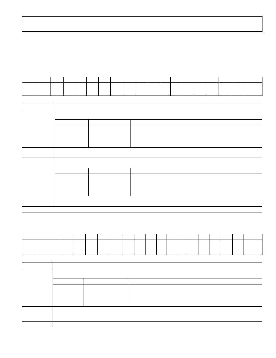
Preliminary Technical Data
AD1986
Rev. 0 | Page 31 of 52
C/LFE DAC VOLUME (REGISTER 0x36)
This register controls the CENTER/LFE DAC gain and mute to the output selector section. The volume register contains five bits,
generating 32 volume steps of -1.5 dB each for a range of +12.0 dB to -34.5 dB.
Note that the left/right association of the CENTER and LFE channels can be swapped at the CODEC outputs by setting the CSWP bit in
Register 74h. These controls remain unchanged regardless of the state of CSWP.
Reg
Name D15
D14
D13
D12
D11
D10
D9 D8 D7 D6
D5
D4 D3 D2 D1 D0 Default
0x36 C/LFE
DAC
Volume
LFEM x
x
LFE4 LFE3 LFE2 LFE1 LFE0 CNTM x x CNT4 CNT3 CNT2 CNT1 CNT0 0x8888
Table 53.
Register Function
Controls the gain of the CENTER channel to the output selector section from +12.0 dB to -34.5 dB. The least significant
bit represents -1.5 dB.
CNTM CNT
[4:0] Function
Default
0
0 0000
+12 dB gain
0
0 1000
0 dB attenuation
Default
0
1 1111
-34.5 dB attenuation
CNT [4:0]
(Center Volume)
1 x
xxxx Muted
CNTM
(Center Mute)
Mutes the center channel.
Default: muted (0x1)
Controls the gain of the LFE channel to the output selector section from +12.0 dB to -34.5 dB. The least significant bit
represents -1.5 dB.
LFEM LFE[4:0]
Function
0
0 0000
+12 dB gain
0
0 1000
0 dB attenuation
Default
0
1 1111
-34.5 dB attenuation
LFE [4:0]
(LFE Volume)
1 x
xxxx Muted
LFEM
(LFE Mute)
Mutes the LFE channel.
Default: muted (0x1)
x Reserved.
Default: 0
SURROUND DAC VOLUME (REGISTER 0x38)
This register controls the SURROUND DAC gain and mute to the output selector section. The volume register contains five bits,
generating 32 volume steps of -1.5 dB each for a range of +12.0 dB to -34.5 dB.
Reg Name
D15 D14 D13 D12 D11 D10 D9 D8 D7 D6 D5 D4 D3 D2 D1 D0 Default
0x18
Surround
DAC
Volume
LM x x
LV4 LV3 LV2 LV1 LV0 RM x x RV4 RV3 RV2 RV1 RV0 0x8888
Table 54.
Register Function
Controls the left/right channel gains of this input to the output selector section from +12 dB to -34.5 dB. The least
significant bit represents -1.5 dB.
L/RM L/RV
[4:0]
Function
Default
0
0 0000
+12 dB gain
0
0 1000
0 dB
Default
0
1 1111
-34.5 dB attenuation
L/RV [4:0]
(Left/Right
Volume)
1 x
xxxx
Muted
L/RM
(Left/Right
Mute)
Mutes the left/right channels independently. Default:
muted
(0x1)
x Reserved.
Default:
0

AD1986
Preliminary Technical Data
Rev. 0 | Page 32 of 52
SPDIF CONTROL (REGISTER 0x3A)
Register 0x3A is a read/write register that controls SPDIF functionality and manages bit fields propagated as channel status (or subframe
in the V-case). With the exception of V, this register should only be written to when the SPDIF transmitter is disabled (SPDIF bit in
Register 0x2A is 0). This ensures that control and status information start up correctly at the beginning of SPDIF transmission.
Reg Name D15 D14 D13 D12 D11 D10 D9 D8 D7 D6 D5 D4 D3 D2 D1
D0 Default
0x3A
SPDIF
Control
V
VCFG SPSR x
L
CC6 CC5 CC4 CC3 CC2 CC1 CC0 PRE COPY
/AUDIO
PRO 20000x
Table 55.
Register Function
Indicates professional use of the audio stream.
PRO State
Default
0
Consumer use of channel
Default
PRO
(Professional)
1
Professional use of channel
Indicates that the data is PCM or another format (such as AC3).
/AUDIO State
0
Data in PCM format
Default
/AUDIO
(Nonaudio)
1
Data in non-PCM format
Allows receivers to make copies of the digital data.
COPY State
0 Copyright
asserted
Default
COPY
(Copyright)
1
Copyright not asserted
Disables filter pre-emphasis.
PRE State
0
Filter pre-emphasis is 50/15
µsec
Default
PRE
(Pre-emphasis)
1 No
pre-emphasis
CC [6:0]
(Category Code)
Programmed according to IEC standards, or as appropriate.
L
(Generation Level)
Programmed according to IEC standards, or as appropriate.
Chooses between 48.0 kHz and 44.1 kHz S/PDIF transmitter rate.
SPSR Transmit
Sample
Rate
0 44.1
kHz
1 48.0
kHz
Default
SPSR
(SPDIF Transmit
Sample Rate)
When asserted, this bit forces the SPDIF stream validity flag (bit < 28 > within each SPDIF L/R subframe) to be controlled by
the validity bit (D15) in Register 0x3A (SPDIF control register).
VCFG
V
Validity Bit State
Reset Default: 0
0
0
Managed by CODEC error detection logic
Default
0
1
Forced high, indicating subframe data is
invalid
1
0
Forced low, indicating subframe data is valid
VCFG
(Validity Force Bit)
1
1
Forced high, indicating subframe data is
invalid
V
(Validity)
This bit affects the validity flag, (bit <28 > transmitted in each SPDIF L/R subframe) and enables the SPDIF transmitter to
maintain connection during error or mute conditions. Note that the VCFG bit (0x3A D14) will force the validity flag high (valid)
or low (invalid). See the VCFG bit description.
V State
0
Each SPDIF subframe (L+R) has bit <28> set to 1
Default
This tags both samples as invalid
1
Each SPDIF subframe (L+R) has bit <28> set to 0 for valid data and 1 for invalid data (error condition)
x Reserved.
Default:
0
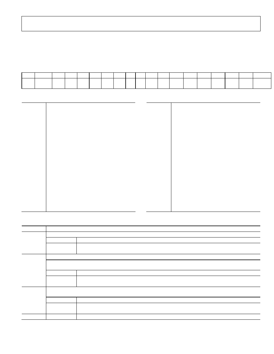
Preliminary Technical Data
AD1986
Rev. 0 | Page 33 of 52
EQ CONTROL REGISTER (REGISTER 0x60)
Register 0x60 is a read/write register that controls equalizer function and data setup. The register also contains the Biquad and coefficient
address pointer, which is used in conjunction with the EQ data register (0x78) to setup the equalizer coefficients. The reset default
disables the equalizer function until the coefficients can be properly set up by the software and sets the symmetry bit to allow equal
coefficients for left and right channels.
Reg Name D15 D14 D13 D12 D11 D10 D9 D8 D7 D6 D5
D4
D3
D2
D1
D0
Default
0x60
EQ
Control
EQM x
x
x
x
x
x x SYM CHS BCA5 BCA4 BCA3 BCA2 BCA1 BCA0 0x8080
Table 56. Biquad and Coefficient Address Pointer
BCA [5,0]
Biquad 0
Coef a0
BCA [5,0] = 011011
Biquad 0
Coef a1
BCA [5,0] = 011010
Biquad 0
Coef a2
BCA [5,0] = 011001
Biquad 0
Coef b1
BCA [5,0] = 011101
Biquad 0
Coef b2
BCA [5,0] = 011100
Biquad 1
Coef a0
BCA [5,0] = 100000
Biquad 1
Coef a1
BCA [5,0] = 011111
Biquad 1
Coef a2
BCA [5,0] = 011110
Biquad 1
Coef b1
BCA [5,0] = 100010
Biquad 1
Coef b2
BCA [5,0] = 100001
Biquad 2
Coef a0
BCA [5,0] = 100101
Biquad 2
Coef a1
BCA [5,0] = 100100
Biquad 2
Coef a2
BCA [5,0] = 100011
Biquad 2
Coef b1
BCA [5,0] = 100111
Biquad 2
Coef b2
BCA [5,0] = 100110
Biquad 3
Coef a0
BCA [5,0] = 101010
Biquad 3
Coef a1
BCA [5,0] = 101001
Biquad 3
Coef a2
BCA [5,0] = 101000
Biquad 3
Coef b1
BCA [5,0] = 101100
Biquad 3
Coef b2
BCA [5,0] = 101011
Biquad 4
Coef a0
BCA [5,0] = 101111
Biquad 4
Coef a1
BCA [5,0] = 101110
Biquad 4
Coef a2
BCA [5,0] = 101101
Biquad 4
Coef b1
BCA [5,0] = 110001
Biquad 4
Coef b2
BCA [5,0] = 110000
Biquad 5
Coef a0
BCA [5,0] = 110100
Biquad 5
Coef a1
BCA [5,0] = 110011
Biquad 5
Coef a2
BCA [5,0] = 110010
Biquad 5
Coef b1
BCA [5,0] = 110110
Biquad 5
Coef b2
BCA [5,0] = 110101
Biquad 6
Coef a0
BCA [5,0] = 111001
Biquad 6
Coef a1
BCA [5,0] = 111000
Biquad 6
Coef a2
BCA [5,0] = 110111
Biquad 6
Coef b1
BCA [5,0] = 111011
Biquad 6
Coef b2
BCA [5,0] = 111010
Table 57.
Register Function
Swaps the blocks that are used for symmetry coefficients. Only valid when the SYM bit is set.
CHS Function
Default
0
Selects left channel coefficients data block
Default
CHS
(Channel
Select)
1
Selects right channel coefficients data block
When set to 1 this bit indicates that the left and right channel coefficients are equal.
This shortens the coefficients setup sequence since only the left channel coefficients need to be addressed and setup. The
right channel coefficients are simultaneously copied into memory.
SYM Function
0
Left and right channels can use different coefficients
SYM
(Symmetry)
1
Indicates that the left and right channel coefficients are equal
Default
When set to 1, this bit disables the equalizer function (allows all data pass-through). The reset default sets this bit to 1
disabling the equalizer function until the biquad coefficients can be properly set.
EQM Function
0
EQ is enabled.
EQM
(Equalizer
Mute)
1
EQ is disabled. Data will pass-thru without change.
Default
x Reserved.
Default:
0

AD1986
Preliminary Technical Data
Rev. 0 | Page 34 of 52
EQ DATA REGISTER (REGISTER 0x62)
This read/write register is used to transfer EQ biquad coefficients into memory. The register data is transferred to, or retrieved from the
address pointed by the BCA bits in the EQ CNTRL register (0x60). Data will only be written to memory, if the EQM bit (Register 0x60
bit 15) is asserted.
Reg
Name
D15 D14 D13 D12 D11 D10 D9 D8 D7 D6 D5 D4 D3 D2 D1 D0 Default
0x62 EQ
Data
CFD15 CFD14 CFD13
CFD12 CFD11 CFD10 CFD9 CFD8 CFD7 CFD6 CFD5 CFD4 CFD3 CFD2 CFD1 CFD0 0xxxxx
Table 58.
Register Function
CFD [15:0]
(Coefficient
Data)
The biquad coefficients are fixed point format values with 16 bits of resolution. The CFD15 bit is the MSB and the CFD0 bit is
the LSB.
MISC CONTROL BITS 2 (REGISTER 0x70)
Reg Name
D15 D14 D13 D12
D11
D10
D9 D8 D7
D6 D5
D4
D3
D2
D1 D0 Default
0x70 Misc
Control
Bits 2
x x x
MVREF
2
MVREF
1
MVREF
0
x x MMDIS
x JSMAP
CVREF
2
CVREF
1
CVREF
0
x x 0x0000
Table 59.
Register Function
CVREF [2:0]
(C/LFE VREF_OUT
Control)
Sets the voltage/state of the C/LFE VREF_OUT signal. VREF_OUT is used to power microphone style devices
plugged into the connected jack circuitry. The VREF_OUT pin must be connected to both the left and right
channels through external resistors to function properly. Selections other than those defined are invalid and
should not be programmed.
C/LFE VREF_OUT Setting
CVREF [2:0]
5.0 AV
DD
3.3 V AV
DD
Default
000
Hi-Z Hi-Z
Default
001
2.25 V
2.25 V
010
0V 0V
100
3.70 V
2.25 V
JSMAP
(Jack Sense Mapping)
The AD1986 supports two different methods of mapping the JACK_SENSE_A/B resistor tree to bits JS [7:0]. Use
these bits to change from the default mapping to the alternate method.
JSMAP Function
0
Default Jack Sense mapping
Default
1
Alternate Jack Sense mapping
MMDIS
(Mono Mute Disable)
Disables the automatic muting of the MONO_OUT pin by jack sense events (see advanced jack sense bits JS [3:0]
(0x76 D [05:04], 0x72 D [05:04]).
MMDIS Function
0
Automute can occur
Default
1
Automute
disabled
MVREF [2:0]
(MIC VREF_OUT)
Sets the voltage/state of the microphone VREF_OUT signal. VREF_OUT is used to power microphone style devices
plugged into the connected jack circuitry. The VREF_OUT pin must be connected to both the left and right
channels through external resistors to function properly. Selections other than those defined are invalid and
should not be programmed.
MIC_1/2 VREF_OUT Setting
MV
REF
[2:0]
5.0 AV
DD
3.3 V AV
DD
000
Hi-Z
Hi-Z
Default
001
2.25 V
2.25 V
010
0 V
0 V
100
3.70 V
2.25 V
x Reserved.
Default: 0
Preliminary Technical Data
AD1986
Rev. 0 | Page 35 of 52
JACK SENSE (REGISTER 0x72)
All register bits are read/write except for JS0ST and JS1ST, which are read only. Important: Please refer to Table 72 to understand how
JACK_SENSE_A and JACK_SENSE_B codec pins translate to JS1and JS0.
Reg Name D15 D14 D13 D12 D11 D10 D9 D8 D7 D6 D5 D4 D3 D2 D1 D0 Default
0x72
Jack
Sense
JS1
SPRD
JS1
DMX
JS0
DMX
JSMT
2
JSMT
1
JSMT
0
JS1
EQB
JS0
EQB
x x JS1
MD
JS0
MD
JS1
ST
JS0
ST
JS1
INT
JS0
INT
0x0000
Table 60.
Register Function
Indicates JS0 has generated an interrupt. Remains set until the software services JS0 interrupt; i.e., JS0 ISR should clear this
bit by writing a 0 to it.
1. Interrupts are generated by valid state changes of JS pins.
2. Interrupt to the system is actually an OR combination of this bit and JS3 JS0 INT.
3. The interrupt implementation path is selected by the INTS bit (Register 0x74).
4. It is also possible to generate a software system interrupt by writing a 1 to this bit.
JS0INT Read
Write
0
JS0 did not generate interrupt
No operation
JS0INT
(JS0
Interrupt
Status)
1
JS0 generated interrupt Clears
JS0INT
bit
Indicates JS1 has generated an interrupt. Remains set until the software services JS1 interrupt; i.e., JS1 ISR should clear this
bit by writing a 0 to it. See JS0INT description above for additional details.
JS1INT Read
Write
0
JS1 did not generate interrupt
No operation
JS1INT
(JS1
Interrupt
Status)
1
JS1 generated interrupt Clears
JS1INT
This bit always reports the logic state of JS0.
On MIC jack sensing: depending on the applications circuit, the logic state for jack sense pins can be the opposite of that on
other jacks. Software needs to be aware of this is interpreting the JS event as a plug in our out event.
JS0ST Function
Default
0
JS0 is low (0)
JS0ST (RO)
(JS0 State
(RO))
1
JS0 is high (1)
This bit always reports the logic state of JS1. MIC jack sensing: depending on the applications circuit, the logic state for JS
pins can be the opposite to the other jacks.
JS1ST Function
0
JS1 is low (0)
JS1ST (RO)
(JS1 State
(read only))
1
JS is high (1)
This bit selects the operation mode for JS0.
JS0MD Function
0
Jack sense mode--JS0INT must be polled by software
Default
JS0MD
(JS0 MODE)
1
Interrupt mode--CODEC will generate an interrupt on JS0 event
This bit selects the operation mode for JS1.
JS1MD Function
0
Jack sense mode--JS1INT must be polled by software
Default
JS1MD
(JS1 MODE)
1
Interrupt mode--CODEC will generate an interrupt on JS1 event
This bit enables JS0 to control the EQ bypass. When this bit is set to 1, JS0 = 1 will cause the EQ to be bypassed.
JS0EQB Function
0
JS0 does not affect EQ
Default
JS0EQB
(JS0 EQ
Bypass
Enable)
1
JS0 = 1 will cause the EQ to be bypassed
This bit enables JS1 to control the EQ bypass. When this bit is set to 1, JS1=1 will cause the EQ to be bypassed.
JS1EQB Function
0
JS1 does not affect EQ
Default
JS1EQB
(JS1 EQ
Bypass
Enable)
1
JS1 = 1 will cause the EQ to be bypassed

AD1986
Preliminary Technical Data
Rev. 0 | Page 36 of 52
Register Function
JSMT [2,0]
(JS Mute
Enable
selector)
These 3 bits select and enable the jack sense muting action. See Table 61.
JS0DMX
(JS0 Down-
Mix Control
Enable)
This bit enables JS0 to control the down-mix function. This function allows a digital mix of 6-channel audio into 2-channel
audio. The mix can then be routed to the stereo LINE_OUT or HP_OUT jacks. When this bit is set to 1, JS0 = 1 will activate the
down-mix conversion. See DMIX description in Register 0x76. The DMIX bits select the down-mix implementation type and
can also force the function to be activated.
JS0DMX Function
0
JS0 does not affect down mix
Default
1
JS0 = 1 activates the 6- to 2-channel down mix
This bit enables JS1 to control the down-mix function (see the JS0DMx description above). When this bit is set to 1, JS1 = 1
will activate the down-mix conversion.
JS1DMX Function
0
JS1 does not affect down-mix
Default
JS1DMX
(JS1 Down-
Mix Control
Enable)
1
JS1 = 1 activates the 6- to 2-channel down-mix
This bit enables the 2-channel to 6-channel audio spread function when JSs are active (Logic State 1). Note that the SPRD bit
can also force the Spread function without being gated by the jack senses. Please see this bit's description in Register 0x76
for a better understanding of the Spread function.
JSSPRD Function
0
JS1 does not affect spread
Default
JSSPRD
(JS Spread
control
enable)
1
J10 = 1 activates spread
x Reserved.
Default: 0
Table 61. Jack Sense Mute Selections (JSMT)
REF JS1
JS0
JSMT2 JSMT1 JSMT0
HP
OUT
LINE
OUT
C/LFE
OUT
SURR
OUT
MONO
OUT NOTES
0
OUT (0)
OUT (0)
0
0
0
ACTIVE
ACTIVE
ACTIVE
ACTIVE
ACTIVE
JS0 and JS1 ignored
1
OUT (0)
IN (1)
0
0
0
ACTIVE
ACTIVE
ACTIVE
ACTIVE
ACTIVE
2
IN (1)
OUT (0)
0
0
0
ACTIVE
ACTIVE
ACTIVE
ACTIVE
ACTIVE
3
IN (1)
IN (1)
0
0
0
ACTIVE
ACTIVE
ACTIVE
ACTIVE
ACTIVE
4
OUT (0)
OUT (0)
0
0
1
ACTIVE
FMUTE
FMUTE
FMUTE
ACTIVE
JS0 no mute action
5
OUT (0)
IN (1)
0
0
1
ACTIVE
FMUTE
FMUTE
FMUTE
ACTIVE
JS1 mutes mono and enables
LINE_OUT + SURR_OUT +
C/LFE
6
IN (1)
OUT (0)
0
0
1
ACTIVE
ACTIVE
ACTIVE
ACTIVE
FMUTE
7
IN (1)
IN (1)
0
0
1
ACTIVE
ACTIVE
ACTIVE
ACTIVE
FMUTE
STANDARD 6 CHAN CONFIG
8
OUT (0)
OUT (0)
0
1
0
FMUTE
ACTIVE
FMUTE
FMUTE
ACTIVE
JS0 no mute action, SWAPPED
HP_OUT and LINE_OUT
9
OUT (0)
IN (1)
0
1
0
FMUTE
ACTIVE
FMUTE
FMUTE
ACTIVE
JS1 mutes mono and enables
HP_OUT + SURR_OUT + C/LFE
10
IN (1)
OUT (0)
0
1
0
ACTIVE
ACTIVE
ACTIVE
ACTIVE
FMUTE
11
IN (1)
IN (1)
0
1
0
ACTIVE
ACTIVE
ACTIVE
ACTIVE
FMUTE
STANDARD 6 CHAN CONFIG
no swap
12
OUT (0)
OUT (0)
0
1
1
**
**
**
**
**
**RESERVED
13
OUT (0)
IN (1)
0
1
1
**
**
**
**
**
14
IN (1)
OUT (0)
0
1
1
**
**
**
**
**
15
IN (1)
IN (1)
0
1
1
**
**
**
**
**
16
OUT (0)
OUT (0)
1
0
0
ACTIVE
FMUTE
FMUTE
FMUTE
ACTIVE
JS0 = 0 and JS1 = 0
enables MONO
17
OUT (0)
IN (1)
1
0
0
ACTIVE
ACTIVE
ACTIVE ACTIVE FMUTE JS1
=
1
enabled
FRONT only
18
IN (1)
OUT (0)
1
0
0
ACTIVE
FMUTE
FMUTE
FMUTE
FMUTE
JS0 = 1 and JS1 = 0
enables all rear
19
IN (1)
IN (1)
1
0
0
ACTIVE
FMUTE
FMUTE
FMUTE
FMUTE
6 CHAN CONFIG with front
jack wrap back

Preliminary Technical Data
AD1986
Rev. 0 | Page 37 of 52
REF JS1
JS0
JSMT2 JSMT1 JSMT0
HP
OUT
LINE
OUT
C/LFE
OUT
SURR
OUT
MONO
OUT
NOTES
20
OUT (0)
OUT (0)
1
0
1
FMUTE
FMUTE
FMUTE
FMUTE
ACTIVE
JS0 no mute action
21
OUT (0)
IN (1)
1
0
1
FMUTE
FMUTE
FMUTE
FMUTE
ACTIVE
JS1 mutes mono and enables
all rear.
22
IN (1)
OUT (0)
1
0
1
ACTIVE
ACTIVE
ACTIVE
ACTIVE
FMUTE
23
IN (1)
IN (1)
1
0
1
ACTIVE
ACTIVE
ACTIVE
ACTIVE
FMUTE
STANDARD 6 CHAN CONFIG
swapped HP_OUT and
LINE_OUT
24
OUT (0)
OUT (0)
1
1
0
**
**
**
**
**
**RESERVED
25
OUT (0)
IN (1)
1
1
0
**
**
**
**
**
26
IN (1)
OUT (0)
1
1
0
**
**
**
**
**
27
IN (1)
IN (1)
1
1
0
**
**
**
**
**
28
OUT (0)
OUT (0)
1
1
1
**
**
**
**
**
**RESERVED
29
OUT (0)
IN (1)
1
1
1
**
**
**
**
**
30
IN (1)
OUT (0)
1
1
1
**
**
**
**
**
31
IN (1)
IN (1)
1
1
1
**
**
**
**
**
FMUTE
= Output is forced to mute independent of the respective volume register setting.
ACTIVE
= Output is not muted and its status is dependent on the respective volume register setting.
OUT
= Nothing is plugged into the jack and therefore the JS status is 0 (via the load resistor pull-down action).
IN
= Jack has plug inserted and therefore the JS status is 1 (via the CODEC JS pin internal pull-up).
SERIAL CONFIGURATION (REGISTER 0x74)
When Register 0x00 is written (soft reset) the SLOT 16, REGM [2:0], SPOVR, SPAL, SPDZ, and SPLNK bits do not reset. All bits are reset
on a hardware reset or power-on reset.
Reg
Name
D15 D14 D13 D12 D11 D10
D9 D8 D7 D6 D5 D4
D3 D2 D1 D0 Default
0x74 Serial
Configuration
SLOT
16
REGM2 REGM1
REGM0 REGM3 OMS2 OMS1 OM0 SPOVR LBKS1 LBKS0 INTS CSWP SPAL SPDZ SP
LNK
0x1001
Table 62.
Register Function
Default
This bit enables the S/PDIF to link with the front DACs for data requesting. When linked the S/PDIF and front DACs should be
set to the same data rate as they both generate data requests at the front DAC's request rate.
SPLNK Function
0
S/PDIF and front DACs are not linked
SPLNK
(S/PDIF
LINK)
1
S/PDIF and front DACs are linked
Default
Sets data fill mode for S/PDIF transmitter FIFO under-runs. When this bit is set to ON (1) the S/PDIF and ADC rates should be
set to the same rate.
SPDZ On
Under-Runs
0
Repeat last sample out the S/PDIF stream
Default
SPDZ
(S/PDIF
DACZ)
1
Forces midscale sample out the S/PDIF stream
SPAL
S/PDIF Transmitter Source
0
Connected to the AC-LINK stream
Default
SPAL
(S/PDIF
ADC Loop
Around)
1
Connected to the digital ADC stream
Swaps the CENTER/LFE channels. Some systems have a swapped external connection for the CENTER and LFE channels.
Setting this bit will swap these channels internal to the CODEC. Note that the CENTER and LFE controls do not change and
remain at the same addresses and bit assignments.
CSWP CENTER
Pin
LFE
Pin
0
CENTER channel
LFE channel
Default
(CSWP
CENTER/LFE
Swap)
1
LFE channel
CENTER channel
This bit selects the audio interrupt implementation path. Note that this bit does not generate an interrupt, rather it steers the
path of the generated interrupt.
INTS Interrupt
Mode
INTS
(Interrupt
Mode
Select)
0
Bit 0 SLOT 12 (modem interrupt)
Default

AD1986
Preliminary Technical Data
Rev. 0 | Page 38 of 52
Register Function
Default
1
Slot 6 valid bit (MIC ADC interrupt)
These bits select the internal digital loop-back path when LPBK bit is active (see Register 0x20).
LBKS [1:0]
Interrupt Mode
00
Loop back through the front DACs
Default
01
Loop back through the SURROUND DACs
10
Loop back through the center and LFE DACs (center
DAC loops back from the ADC left channel, the LFE
DAC from the ADC right channel)
LBKS [1:0]
Loop-Back
Selection
11 Reserved
Use this bit to enable S/PDIF operation even if the external S/PDIF detection resistor is not installed.
SPOVR S/PDIF
Detection
0
External resistor determines the presence of
S/PDIF
Default
SPOVR
(S/PDIF
Enable
Override)
1
Enable S/PDIF operation
Selects the source of the microphone gain noost amplifiers. These bits work in conjuction with the 2CMIC (0x76 D06),
MS (0x20 D08), and MMIX (0x7A D08) bits.
OMS [2:0]
Left Channel
000 MIC
pins
Default
001
LINE_IN pins
01x C/LFE
pins
100
Mix of MIC and C/LFE pins
101
Mix of MIC and LINE_IN pins
110
Mix of LINE_IN and C/LFE pins
OMS [2:0]
Optional
Microphone
Selector
111
Mix of MIC, LINE_IN and C/LFE pins
REGM [3:0]
Bit mask indicating which CODEC is being accessed in a chained CODEC configuration.
REGM0--Master CODEC register mask
Default
REGM1--Slave 1 CODEC register mask
REGM2--Slave 2 CODEC register mask
REGM3--Slave 3 CODEC register mask
SLOT 16
Enable 16-bit slot mode: SLOT16 makes all AC link slots 16 bits in length, formatted into 16 slots. This is a preferred mode for
DSP serial port interfacing.
SLOT 16
Function
0
Standard AC '97 operation
Default
1
All ac link S slots are 16 bits
x Reserved
Default:
0

Preliminary Technical Data
AD1986
Rev. 0 | Page 39 of 52
MISC CONTROL BITS 1 (REGISTER 0x76)
Reg Name
D15 D14
D13
D12 D11 D10 D9
D8
D7
D6
D5
D4 D3
D2
D1
D0
Default
76h
Misc Control Bits 1
DACZ
AC97NC
MSPLT
SODIS
CLDIS
x
DMIX1 DMIX0 SPRD 2CMIC SOSEL SRU LISEL1 LISEL0 MBG1 MBG0 6010
Table 63.
Register Function
These two bits allow changing both MIC preamp gain blocks from the nominal 20 dB gain boost. Both MIC_1/2
and MIC_2 preamps will be set to the same selected gain. This gain setting only takes affect while bit D6 (M20)
on the MIC volume register (0x0E) is set to 1, otherwise the MIC boost blocks have a gain of 0 dB.
MGB [1:0]
Microphone Boost Gain
Default
00 20
dB
Default
01 10
dB
10 30
dB
MBG [1:0]
(MIC Boost Gain Select
Register)
11 Reserved
Selects the source of the internal LINE_IN signals.
LISEL [1:0]
LINE_IN Selection
00 LINE_IN
pins
Default
01
SURROUND pins--Places SURROUND outputs in Hi-Z state
LISEL [1:0]
(LINE_IN Selector)
1x MIC_1/2
pins
Controls all DAC sample rate locking.
SRU Surround
State
0
All DAC sample rates are locked to the front sample rate
SRU
(Sample Rate Unlock)
1
Front, surround and LFE sample rates can be set independently
Default
Selects either the surround DAC or analog mixer as the source driving the SURROUND output pin amplifier.
SOSEL Surround
Source
0 Surround
DACs
Default
SOSEL
(Surround Amplifier
Input Selection)
1 Analog
Mixer
2CMIC
(2-Channel MIC Select)
Used in conjunction with the OMS [2:0] (0x74 D10:08]), MS (0x20 D08), and MMIX (0x7A D02) bits to set the
microphone selection. This bit enables simultaneous recording from MIC_1 and MIC_2 inputs, using a stereo
microphone array. If the MMIX (0x7A D02) bit is set this bit is ignored.
2CMIC
2 Channel MIC State
0
Both outputs are driven by the left channel of the selector
Default
1
Stereo operation, the left and right channels are driven
separately
SPRD
(Spread Enable)
This bit enables spreading of 2-channel media to all 6-output channels. This function is implemented in the
analog section by using the output selector controls lines for the center/LFE, surround and LINE_OUT output
channels. The jack sense pins can also be setup to control (gate) this function depending on the JSSPRD bit (see
Register 0x72). The SPRD bit operates independently and does not affect the LOSEL and HPSEL operation.
SPRD Spread
State
0
No spreading occurs unless activated by jack sense
Default
1
The SPDR selector drives the center and LFE outputs from the
MONO_OUT
CLDIS
(C/LFE Output Enable)
Controls the Hi-Z state of the SURROUND_L/R output pins. Pins are placed into a Hi-Z mode by software control
or when they are selected as inputs to the MIC_1/2 selector (see the OMS [2:0] bits 740x D [10:08]).
CLDIS
C/LFE Output State
0
Outputs
enabled
Default
1
Outputs
tristated

AD1986
Preliminary Technical Data
Rev. 0 | Page 40 of 52
Register Function
DMIX [1:0]
(DOWN MIX Mode
Select)
Provides analog down-mixing of the center, LFE and/or surround channels into the mixer channels. This allows
the full content of 5.1 or quad media to be played through stereo headphones or speakers. The jack sense pins
can also be setup to control (gate) this function depending on the JS0DMx and JS1DMx bits (0x72 D [14:13]).
DMIX [1:0]
Down-Mix State
0x
No down-mix unless activated by jack sense
Default
10
Selects 6-to-4 down-mix. The center and LFE channels are
summed equally into the Mixer L/R channels
11
Selects 6-to-2 down-mix. In addition to the center and LFE
channels, the SURROUND channels are summed into the
mixer L/R channels
Controls the Hi-Z state of the SURROUND output pins. Pins are placed into a Hi-Z mode by software control or
when they are selected as inputs to the LINE_IN selector (see the LISEL [1:0] bits 0x76 D [03:02]).
CLDIS SURROUND_OUT
State
0 Outputs
enabled
Default
SODIS
(Surround Output
Enable)
1
Outputs tri-stated (Hi-Z)
MSPLT
(RO)
(Mute Split)
Separates the left and right mutes on all volume registers. This bit is read-only 1 (one) on the AD1986 indicating
that mute split is always enabled.
AC `97NC (RO)
(AC `97 No Compatibility
Mode)
Changes addressing to ADI model (vs. true AC '97 definition). This bit is read-only 1 (one) on the AD1986
indicating that ADI addressing is always enabled.
Determines DAC data fill under starved condition.
DACZ
DAC Fill State
0
DAC data is repeated when DACs are starved for data
Default
DACZ
(DAC Zero-Fill)
1
DAC data is zero-filled when DACs are starved for data
x Reserved.
Default:
0
ADVANCED JACK SENSE (REGISTER 0x78)
All register bits are read/write except for JSxST bits, which are read-only. Important: Please refer to Table 72 to understand how
JACK_SENSE_A and JACK_SENSE_B codec pins translate to JS7...JS2.
Reg Name
D15 D14 D13 D12 D11 D10 D9 D8 D7 D6 D5 D4 D3 D2 D1 D0 Default
0x78
Advanced
Jack Sense
JS7
ST
JS7
INT
JS6
ST
JS6
INT
JS5
ST
JS5
INT
JS4
ST
JS4
INT
JS4-
7H
x
JS3
MD
JS2
MD
JS3
ST
JS2
ST
JS3
INT
JS2
INT
0xxxxx
Table 64.
Register Function
JS [7:2] INT
Indicates JSx has generated an interrupt. Remains set until the software services JSx interrupt; i.e., JSx ISR should clear
this bit by writing a 0 to it.
1. Interrupts are generated by valid state changes of JSx.
2. Interrupt to the system is actually an OR combination of this bit and JS7 JS0 INT.
3. Interrupt implementation path is selected by the INTS bit (Register 0x74).
4. It is also possible to generate a software system interrupt by writing a 1 to this bit.
JS [7:4] INT
Read
Write
Default
0
JSx logic is not interrupting
Clears JSx interrupt
Default
1
Sx logic interrupted
Generates a software interrupt
This bit always reports the logic state of JS7 thru 4 detection logic.
JS [7:4] ST
Jack State
0
No jack present
JS [7:4] ST (RO)
1 Jack
detected
This bit selects the operation mode for JS2 and JS3.
JS [3:2] MD
Interrupt Mode
JS [3:2] MD
0
Jack Sense Mode--jack sense state requires software polling
Default
1
Interrupt Mode--jack sense evetns will generate interrupts

Preliminary Technical Data
AD1986
Rev. 0 | Page 41 of 52
Register Function
This bit selects the audio interrupt implementation path (for JS4 to 7). This bit does not generate an interrupt, rather it
steers the path of the generated interrupt.
JS4 to 7H
Interrupt Mode--JS4 to 7
0
Bit 0 SLOT 12 (modem interrupt)
Default
JS4≠7H
Interrupt
Mode Select
1
Slot 6 valid bit (MIC ADC interrupt)
x Reserved
Default:
0
MISC CONTROL BITS 3 (REGISTER 0x7A)
Reg Name
D15 D14
D13
D12 D11 D10
D9
D8
D7 D6 D5 D4
D3 D2 D1 D0 Default
0x7A
Misc Control Bits 3 JSINVB
HPSEL1
HPSEL0 LOSEL JSINVA LVREF
2 LVREF1 LVREF
0
x x x LOHPEN
GPO
MMIX
x x 0x0000
Table 65.
Register Function
Used in conjunction with the OMS [2:0] (0x74 D10:08), MS (0x20 D08), and 2CMIC (0x76 D06) bits to mix the microphone
selector left/right channels. If the MMIX bit is set, the 2CMIC and MS bits are ignored.
MMIX Function
Default
0
Microphone channels are not mixed
Default
1
The left/right channels from the microphone selector are mixed
MMIX
Sets the state of the GPO pin
GPO
GPO Function
0
GPO pin is at logic low (DV
SS
) Default
1
GPO pin is at logic high (DV
DD
)
LOHPEN
Enables the headphone drive on the LINE_OUT pins. Disabling the headphone drive is the same as powering it down (see
the PR6 bit (0x26 D14)).
LOHPEN Function
0
LINE_OUT headphone drive is disabled
Default
1
LINE_OUT headphone drive is enabled
LVREF [2:0]
(Line In
VREF_OUT)
Sets the voltage/state of the LINE_IN VREF_OUT signal. VREF_OUT is used to power microphone style devices plugged into
the connected jack circuitry. The VREF_OUT pin must be connected to both the left and right channels through external
resistors to function properly. Selections other than those defined are invalid and should not be programmed.
LINE_IN VREF_OUT Setting
LVREF [2:0]
5.0 AV
DD
3.3 V AV
DD
000
Hi-Z
Hi-Z
Default
001
2.25 V
2.25 V
010
0V
0
V
100
3.70 V
2.25 V
This bit allows the LINE_OUT output amplifiers to be driven by the mixer or the surround DACs. The main purpose for this is
to allow swapping of the frontand surround channels to make better use of the SURR/HP_OUT output amplifiers. This bit
should normally be used in tandem with the HPSEL bit (see below).
LOSEL
(LINE_OUT
Amplifiers
Input Select)
LOSEL LINE_OUT
Select
0
LINE_OUT amplifiers are driven by the
analog mixer outputs
Default
1
LINE_OUT amplifiers are driven by the
surround DAC
SENSE_A: Select the style of switches used on the audio jacks connected to Sense A.
JSINVA
Jack Sense
Invert
JSINVA
Jack Sense Invert--SENSE_A
0
SENSE_A configured for normally-
open (NO) switches
Default
1
SENSE_A configured for normally-closed
(NC) switches

AD1986
Preliminary Technical Data
Rev. 0 | Page 42 of 52
Register Function
This bit allows the headphone power amps to be driven from the surround DACs, C/LFE DACs, or from the mixer outputs.
HPSEL [1:0]
HP_OUT Selection
00
Outputs are driven by the mixer
outputs
Default
01
Outputs are driven by the surround
DACs
HPSEL [1:0]
(Headphone
Amplifier
Input Select)
1x
Outputs are driven by the C/LFE DACs
SENSE_B: Select the style of switches used on the audio jacks connected to Sense B.
JSINVB
Jack Sense Invert--SENSE_B
0
JACK_SENSE_B configured for normally-
open (NO) switches
Default
JSINVB
(Jack Sense
Invert)
1
JACK_SENSE_B configured for normally-
closed (NC) switches
x Reserved.
Default:
0
VENDOR ID REGISTERS (REGISTER 0x7C to 0x7E)
Reg
Name D15
D14
D13
D12
D11
D10
D9
D8
D7 D6 D5 D4 D3 D2 D1 D0 Default
0x7C Vendor
ID 1
F7 F6 F5
F4 F3 F2 F1
F0
S7 S6 S5 S4 S3 S2 S1 S0 0x4144
0x7E Vendor
ID 2
T7 T6 T5
T4 T3 T2 T1
T0
REV7
REV6
REV5
REV4 REV3 REV2 REV1 REV0 0x5378
Table 66.
Register Function
S [7:0]
This register is ASCII encoded to A.
F [7:0]
This register is ASCII encoded to D.
T [7:0]
This register is ASCII encoded to S.
REV [7:0]
This register is set to 0x78, identifying the AD1986.
CODEC CLASS/REVISION REGISTER (REGISTER 0x60)
Reg Name
D15 D14 D13 D12 D11 D10 D9 D8 D7 D6 D5 D4 D3 D2 D1 D0 Default
0x601
CODEC
Class/Rev
x x x
CL4 CL3 CL2 CL1 CL0 RV7 RV6 RV5 RV4 RV3 RV2 RV1 RV0 0x0002
Table 67.
Register Function
Default
RV [7:0]
(Revision ID:
(RO))
These bits specify a device specific revision identifier. The vendor chooses this value. Zero is an acceptable
value. This field should be viewed as a vendor defined extension to the CODEC ID. This number changes
with new CODEC stepping of the same CODEC ID. This number will increment with each stepping/rev. of
the CODEC chip.
The AD1986 will return 0x00 from this register. This is a CODEC vendor specific field to define software
compatibility for the CODEC. Software reads this field together with CODEC vendor ID (Register 7C≠0x7E)
to determine vendor specific programming interface compatibility. Software can rely on vendor specific
register behavior to be compatible among vendor CODECs of the same class.
0x00
Field not implemented
CL [4:0]
(CODEC
Compatibility
Class (RO))
0x01-0x1F
Vendor specific compatibility class code
x Reserved.
Default: 0
Preliminary Technical Data
AD1986
Rev. 0 | Page 43 of 52
PCI SUBSYSTEM VENDOR ID REGISTER (REGISTER 0x62, PAGE 01)
This register is only reset by power-on. It is used by the BIOS to store configuration information (per AC '97 Revision 2.3 specification)
and must not be reset by soft or hardware resets.
Reg Name
D15 D14 D13 D12 D11 D10 D9 D8 D7 D6 D5 D4 D3 D2 D1 D0 Default
0x621 PCI
SVID
PVI15 PVI14 PVI13
PVI12 PVI11 PVI10 PVI9 PVI8 PVI7 PVI6 PVI5 PVI4 PVI3 PVI2 PVI1 PVI0 0xFFFF
Table 68.
Register Function
PVI [15:0]
PCI Sub
System
Vendor ID
Optional per AC `97 specifications, should be implemented as read/write on AD1986.
This field provides the PCI subsystem vendor ID of the audio or modem subassembly vendor (i.e., CNR manufacturer,
motherboard vendor). This is NOT the CODEC vendor PCI vendor ID or the AC '97 controller PCI vendor ID. If data is not
available it should return 0xFFFF.
PCI SUBSYSTEM DEVICE ID REGISTER (REGISTER 0x64, PAGE 01)
This register is only reset by power-on. It is used by the BIOS to store configuration information (per AC'97 v2.3 specification) and must
not be reset by soft or hardware resets.
Reg Name D15 D14 D13 D12 D11 D10 D9 D8 D7 D6 D5 D4 D3 D2 D1 D0 Default
0x641 PCI
SID PI15 PI14 PI13
PI12 PI11 PI10 PI9 PI8 PI7 PI6 PI5 PI4 PI3 PI2 PI1 PI0 0xFFFF
Table 69.
Register Function
PI [15:0]
(PCI Vendor
ID)
Optional per AC `97 specifications, should be implemented as read/write on the AD1986. This field provides the PCI
subsystem ID of the audio or modem subassembly (i.e., CNR model, motherboard SKU). This is NOT the CODEC vendor PCI
ID or the AC '97 controller PCI ID. Information in this field must be available, because the AC '97 controller reads when the
CODEC ready is asserted in the AC link. If data is not available it should return FFFFh.
FUNCTION SELECT REGISTER (REGISTER 0x66, PAGE 01)
This register is used to select which function (analog I/O pins), information and I/O (
0x
6801), and sense (
0x
6A01) registers apply to it.
The AD1986 associates FC =
0x
0 with surround functions and FC =
0x0
1 with front functions. These are changed in the AD1986 to align
with the new device pin-out and to separate LINE_OUT functions.
Reg Name
D15 D14 D13 D12 D11 D10 D9 D8 D7 D6 D5 D4 D3 D2 D1 D0 Default
0x661
Function
Select
x x x x x x x
x
x
x
x
FC3
FC2
FC1
FC0
T/R
0x0000

AD1986
Preliminary Technical Data
Rev. 0 | Page 44 of 52
Table 70.
Register Function
T/R
(FIP or Ring
Selection Bit)
This bit sets which jack conductor the sense value is measured from. Software will program the corresponding rng/tp
selector bit together with the I/O number in bits FC [3:0]. Once software programs the value and properly reads it back to
confirm selection and implementation, it will access the rest of the bits fields in the descriptor. Mono inputs and outputs
should report the relevant function and sense information when T/R is set to 0 (tip). The FIP bit should report 0 (Page
0x01, Register 0x68, Bit 0 reports no function information present) when T/R is set to a 1 on a mono input or output.
T/R Function
0
Tip (left channel)
Default
1
Ring (right channel)
These bits specify the type of audio function described by this page. These bits are read/write and represent current
AC '97 Revision 2.2 defined I/O capabilities. Software will program the corresponding I/O number in this field together
with the tip/ring selector bit T/R. Once software programs the value and properly reads it back to confirm selection and
implementation, it will access the rest of the bits fields in the descriptor.
FC [3:0]
Function
FC [3:0]
Function Code
Bits
0x0
DAC 1 (master out). maps to front DACs (L/R)
Default
0x1
DAC 2 (AUX out). maps to surround DACs (L/R)
0x2
DAC 3 (C/LFE). maps to C/LFE DACs
0x3
S/P-DIF
out
0x4
Phone
in
0x5
MIC_1 (Mic select = 0)
0x6
MIC_2 (Mic select = 1)
0x7
Line
in
0x8
CD
in
0x9
Video in
Not supported on the AD1986
0xA
Aux
in
0xB
Mono
out
0xC
Headphone
ut
0xD≠0xF
Reserved
x Reserved.
Default:
0
INFORMATION AND I/O REGISTER (REGISTER 0x68, PAGE 01)
This address represents multiple registers (one for each supported function code (FC [3:0] bits (
0x
66 D [04:01])). These values are only
reset by power-on. It is used by the BIOS to store configuration information (per AC '97 Revision 2.3 specifications) and must not be reset
by soft or hardware resets.
Reg Name
D15 D14 D13 D12 D11 D10 D9 D8 D7 D6 D5 D4 D3 D2 D1 D0 Default
0x681
Information
and I/O
G4 G3 G2 G1 G0 INV DL4 DL3 DL2 DL1 DL0 IV x x x FIP 0xxxxx
Table 71.
Register Function
FIP (RO)
(Function
Information
Present)
CODEC default. When set to a 1, this bit indicates that the G [4:0], INV, DL [4:0] (in Register 0x681), and ST [2:0] (in
Register 0x6A1) bits are supported and are read/write capable. This bit set to a 0 indicates that the G [4:0], INV, DL [4:0], and
ST [2:0] bits are not supported, and are read-only with a value of 0. Mono inputs and outputs should report the relevant
function and sense information when T/R is set to 0 (tip). The FIP bit should report 0 (Page 0x01, Register 0x68, Bit 0 reports
no function information present) when T/R is set to a 1 on a mono input or output.
FIP Function
0
Function information not supported
Power-on default
1
Function information supported

Preliminary Technical Data
AD1986
Rev. 0 | Page 45 of 52
Register Function
Indicates whether a sensing method is provided by the CODEC and if information field is valid. This field is updated by the
CODEC.
IV
(Information
Valid Bit)
IV Function
0
After CODEC reset de-assertion, it indicates the CODEC does NOT provide sensing logic and this bit will be
Read-Only. After a sense cycle is completed indicates that no information is provided on the sensing method.
1
After CODEC reset de-assertion, it indicates the CODEC provides sensing logic for this I/O and this bit is
Read/Write. After clearing this bit by writing 1, when a sense cycle is completed indicates that there is valid
information in the remaining descriptor bits. Writing 0 to this bit has no effect.
DL [4:0]
(Buffer
Delays,
Read/Write)
A number representing a delay measurement for the input and output channels. The default value is the delay internal to
the CODEC. The BIOS may add to this value the known delays external to the CODEC, such as for an external amplifier, logic,
etc. Software will use this value to accurately calculate audio stream position with respect to what is been reproduced or
recorded. These values are in 20.83 microsecond (1/48000 second) units. For output channels, this timing is from the end of
AC link frame in which the sample is provided, until the time the analog signal appears at the output pin. For input streams,
this is from when the analog signal is presented at the pin until the representative sample is provided on the AC link. Analog
to analog paths are not considered in this measurement. The measurement is a typical measurement, at a 48 KHz sample
rate, with minimal in-CODEC processing (i.e., 3D effects are turned off.) An example of an audio output delay is filter group
delay and FIFO or other sample buffers in the path. So when an audio PCM sample is written to the CODEC in an AC '97
frame it will be delayed before the output pin is updated to that value.
DL [4:0]
Function
0x00
Information
not
provided
0x01-0x1E
Buffer delay: 20.83 µs per unit
0x1F
Reserved
Indicates that the CODEC presents a 180 degree phase shift to the signal. This bit is only reset by a power-on reset, since it is
typically written by the system BIOS and is not reset by CODEC hard or soft resets as long as power remains applied to the
CODEC.
INV Function
0
No phase shift
INV
(Inversion
Bit,
Read/Write,
CODEC
Default)
1
Signal is shifted by 180∞ from the source signal
G [4:0]
(Gain Bits
(Read/Write))
The CODEC updates these bits with the gain value (dB relative to level-out) in 1.5 dBV increments, not including the volume
control gains. For example, if the volume gain is to 0 dB, then the output pin should be at the 0 dB level. Any difference in
the gain is reflected here. When relevant, the BIOS updates this bit to take into consideration external amplifiers or other
external logic that it knows about. G [3:0] indicates the magnitude of the gain. G [4] indicates whether the value is a gain or
attenuation--essentially it is a sign bit. These bits are only reset by a power-on reset as they are typically written by the
system BIOS and are not reset by CODEC hard or soft resets as long as power remains applied to the CODEC.
G4
G [3:0]
Gain/Attenuation (dB Relative to Level-Out)
0
0000
0
dB
0001
+1.5
dB
0
...
+1.5 dB ◊ G [3:0]
1111
+24.0
dB
0001
-1.5
dB
1
...
-1.5 dB ◊ G [3:0]
1111
-24.0
dB
x
Reserved
Default:
0

AD1986
Preliminary Technical Data
Rev. 0 | Page 46 of 52
SENSE REGISTER (REGISTER 0x6A, PAGE 01)
This address represents multiple registers (one for each supported function code (FC [3:0] bits (
0x
66 D [04:01])). The ST [2:0] bits are
only reset by power-on. They are used by the BIOS to store configuration information (per AC '97 Revision 2.3 specifications) and must
not be reset by soft, hard or hardware resets. The remaining bits are the result of the last sense operation performed by the impedance
sensing circuitry.
Reg Name
D15 D14 D13 D12 D11 D10 D9 D8 D7 D6 D5 D4 D3 D2 D1 D0 Default
0x6A1
Sense
Register
ST2 ST1 ST0
S4 S3 S2 S1 S0 OR1 OR0 SR5 SR4 SR3 SR2 SR1 SR0 0xxxxx
Table 72.
Register Function
Default
SR [5:0] (RO)
(Sense Result
Bits, RO)
These bits are used to report a vendor specific fingerprint or value. (resistance, impedance, reactance,
etc. Used with the OR bits which are the multiplying factor.
Default: 0
These bits indicate the order the sense result bits SR [5:0] are using. For example, if measuring resistance SR = 1/OR =
11: the result is 1 K.
OR [1:0]
Order Value
00 10
0
--SR bits indicate the actual impedance in ohms
Default
01 10
1
--SSR bits indicate the impedance in ohms ◊ 10
10 10
2
--SR bits indicate the impedance in ohms ◊ 100
OR [1:0] (RO)
(Order Bits)
11 10
3
--SSR bits indicate the impedance in ohms ◊ 1,000
S [4:0] (RO)
Sensed bits meaning relates to the I/O being sensed as input or output. Read only. Sensed bits (when output sense
cycle initiated). This field allows for the reporting of the type of output peripheral/device plugged in the jack. Values
specified below should be interrogated with the SR [5:0] and OR [1:0] for accurate reporting.
S [4:0]
Sense Value
0x00
Data not valid. Indicates that the reported value(s) is invalid
0x01
No connection. Indicates that there are no connected devices
Default
0x02
Indicates a specific fingerprint value for devices that are not specified or are
unknown
0x03
Speakers (8 )
0x04
Speakers (4 )
0x05
Powered
speakers
0x06
Stereo
headphone
0x07
SPDIF
out
(electrical)
0x08
SPDIF
out
(TOS)
0x09
Mono headset (mono speaker left channel and mic. Read Functions 5 and 6 for
matching microphone)
0x0A
Allows a vendor to report sensing other type of devices/peripherals. SR [5:0]
together with OR [1:0] provide information regarding the type of device sensed
0x0B≠0x0E
Reserved
0x0F
Unknown (use fingerprint)
0x10≠0x1F
Reserved
S [4:0] (RO)
Sensed bits (when input sense cycle initiated). This field allows for the reporting of the type of input peripheral/device
plugged in the jack. Values specified below should be interrogated with the SR [5:0] and OR [1:0] bits for accurate
reporting.
ST [2:0]
Sense Value
0x10
Data not valid. Indicates that the reported value(s) is invalid
0x11
No connection. Indicates that there are no connected devices
Default
0x12
Indicates a specific fingerprint value for devices that are not specified or are
unknown
0x13
Microphone
(mono)

Preliminary Technical Data
AD1986
Rev. 0 | Page 47 of 52
Register Function
Default
0x14
Microphone
(stereo)
0x15
Stereo line in (CE device attached)
0x16
Mono line in (CE device attached)
0x17
SPDIF In (electrical)
0x18
SPDIF In (TOS)
0x19
Headset (mono speaker left channel and mic.) Read Functions 0 to 3 for matching
DAC out
0x1A
Allows a vendor to report sensing other types of devices/peripherals. SR [5:0]
together with OR [1:0] provide information regarding the type of device sensed
0x1B≠0x1E
Reserved
0x1F
Unknown (use fingerprint)
ST [2:0]
(Connector/Jack
location Bits,
Read/Write)
This field describes the location of the jack in the system. This field is updated by the BIOS. This bits is only reset by a
power-on reset as it is typically written by the system BIOS and is not reset by CODEC hard or soft resets as long as
power remains applied to the CODEC.
ST [2:0]
Jack Location
0x0
Rear I/O panel
Power-on
default
0x1
Front
panel
0x2
Motherboard
0x3
Dock/external
0x4≠0x6
Reserved
0x7
No connection/unused I/O

AD1986
Preliminary Technical Data
Rev. 0 | Page 48 of 52
JACK PRESENCE DETECTION
The AD1986 uses two jack sense lines for presence detection on
up to eight external jacks. These lines, combined with the
device detection circuitry, enable software to determine
whether there is a device plugged into the circuit and what type
of device it is. With this feature, software can reconfigure jacks
and amplifiers as necessary to insure proper audio operation.
Jack presence is detected using a resistor tree arrangement. Up
to four jacks can be sensed on a single sense line by using a
different value resistance for each jack between the sense line
and ground (AV
SS
). Each sense line must have a single 2.49k 1%
resistor connected between the sense line and AV
DD
. The
specific resistor values for each jack are shown in Table 73. One
percent tolerance resistors should be used for all jack presence
circuitry to insure accurate detection.
AUDIO JACK STYLES (NC/NO)
The jack sense lines on the AD1986 can be programmed for use
with normally-open (NO) or normally closed (NC) switch
types. Current standard stereo audio jacks have wrap-back pins
that are normally closed. New audio jacks use isolated, normally
open switches, which are required for resistive ladder jack
presence detection. Each sense group (A or B) must have the
same style of jack for presence detection to function correctly.
However, the group (A or B) sense type can be programmed
separately to accommodate systems with different styles of jacks
on the front versus rear panel.
The AD1986 defaults to the isolated, normally open switch
types on power up. The jack sense style for SENSE_A is
controlled by the JSINVA bit (Register.
0x
7A D11). The jack
sense style for SENSE_B is controlled by the JSINVB bit
(Register
0x
7A D15). Writing a 1 to these bits will configure the
corresponding sense circuit for normally closed instead of
normally open switch types.
Wrap-back jacks cannot be used in microphone-capable cir-
cuits. For this reason isolated switches are recommended. The
codec defaults to sensing NO style switches and this method is
preferred.
Normally-Open Switches
If a connection is not present
, do not install the sense resistor
pertaining to that connection.
If a connection is present, but there is no related switch (such
as an internal connection)
, install the sense resistor pertaining
to that connection.
Normally Closed Switches
Connections capable of MIC bias require isolated switches to
function correctly. When using normally closed, wrap-back
switches, the jack resistor must be split into two values. One
value connects the sense line to the jack switch and the other
connects the related audio connection to AV
SS
. The total
resistance (sense line to AV
SS
) must equal the value specified in
Table 73.
If a connection is not present
, install the sense resistors
pertaining to that connection.
If a connection is present, but there is no related switch (such
as an internal connection)
, do not install the sense resistors
pertaining to that connection.
Table 73. Jack Sense Mapping
JACK_SENSE_A
JACK_SENSE_B
Resister (1% tolerance)
Mnemonic Jack JS
Mnemonic
Jack JS
4.99k
D
JS7
LINE
OUT
H
JS0
10.0k LINE
IN
C
JS4
C/LFE
G
JS3
20.0k MIC_1/2
B
JS5
SURROUND
F
JS2
40.2k
HP_OUT A JS1 AUX
IN
E JS6

Preliminary Technical Data
AD1986
Rev. 0 | Page 49 of 52
MICROPHONE SELECTION/MIXING
G
MIC 1
CENTER
LINE IN L
MIC 2
LFE
LINE IN R
G
MIC LEFT
MIC RIGHT
MIC Select: OMS[2:0]
0x74 D10-D08
DEF=000 (MIC 1/2)
000-MIC 1/2
001-Line In
01x-C/LFE
100-MIC+C/LFE
101-MIC+Line In
110-C/LFE+Line In
111-MIC+C/LFE+Line
NID: 0x0F
NID: 0x27
NID: 0x28
NID: 0x29
NID: 0x2A
NID: 0x2B
NID: 0x11
MIC Boost: AC97
M20 0x0E D6 DEF=0
MGB[1:0] 0x76 D[1:0] DEF=00
MGB
M20
[1:0]
Gain
0
xx
0dB
1
00
+20dB
1
01
+10dB
1
10
+30dB
1
11
reserved
Azalia
MGBL[1:0] 0x70 D[1:0]
MGBR[1:0} 0x70 D[14:13]
MGBL/R
[1:0]
Gain
00
0dB
01
+10dB
10
+20dB
11
+30dB
MIC Swap: AC97
MS 0x20 D08 DEF=0
2CMIC 0x76 D06 DEF=0
MMIX 0x7A D02 DEF=0
Azalia
MSWP[2:0] 0x7A D02:00
MMIX
2CMIC MS
MSWP2 MSWP1 MSWP0 Right
Left
0
0
0
MIC 1
MIC 1
0
0
1
MIC 2
MIC 2
0
1
0
MIC 2
MIC 1
0
1
1
MIC 1
MIC 2
1
x
x
MIC 1+2 MIC 1+2
Figure 10. Microphone Selection/Mixing Block Diagram
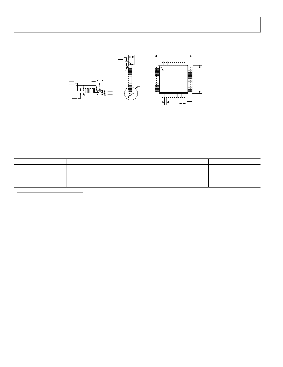
AD1986
Preliminary Technical Data
Rev. 0 | Page 50 of 52
OUTLINE DIMENSIONS
TOP VIEW
(PINS DOWN)
1
12
13
25
24
36
37
48
0.27
0.22
0.17
0.50
BSC
7.00
BSC SQ
SEATING
PLANE
1.60
MAX
0.75
0.60
0.45
VIEW A
9.00 BSC
SQ
PIN 1
0.20
0.09
1.45
1.40
1.35
0.08 MAX
COPLANARITY
VIEW A
ROTATED 90∞ CCW
SEATING
PLANE
10∞
6∞
2∞
7∞
3.5∞
0∞
0.15
0.05
COMPLIANT TO JEDEC STANDARDS MS-026BBC
Figure 11. 48-Lead Low Profile Quad Flat Package [LQFP]
(ST-48)
Dimensions shown in millimeters
ORDERING GUIDE
Model
Temperature Range
Package Description
Package Option
AD1986JSTZ
1
0∞C to +70∞C
48-Lead LQFP, Tray
ST-48
AD1986JSTZ
1
-REEL
0∞C to +70∞C
48-Lead LQFP, Reel
ST-48
AD1986BSTZ
1
≠40∞C to +85∞C
48-Lead LQFP, Tray
ST-48
AD1986BSTZ
1
-REEL
≠40∞C to +85∞C
48-Lead LQFP, Reel
ST-48
1
Z = Pb-free part.

Preliminary Technical Data
AD1986
Rev. 0 | Page 51 of 52
NOTES

AD1986
Preliminary Technical Data
Rev. 0 | Page 52 of 52
NOTES
© 2004 Analog Devices, Inc. All rights reserved. Trademarks and
registered
trademarks are the property of their respective owners.
D04785-0-10/04(0)