REV. 0
Information furnished by Analog Devices is believed to be accurate and
reliable. However, no responsibility is assumed by Analog Devices for its
use, nor for any infringements of patents or other rights of third parties
which may result from its use. No license is granted by implication or
otherwise under any patent or patent rights of Analog Devices.
a
Low Voltage, Resistor Programmable
Thermostatic Switch
AD22105
© Analog Devices, Inc., 1996
One Technology Way, P.O. Box 9106, Norwood, MA 02062-9106, U.S.A.
Tel: 617/329-4700
Fax: 617/326-8703
FEATURES
User-Programmable Temperature Setpoint
2.0 C Setpoint Accuracy
4.0 C Preset Hysteresis
Wide Supply Range (+2.7 V dc to +7.0 V dc)
Wide Temperature Range (≠40 C to +150 C)
Low Power Dissipation (230 W @ 3.3 V)
APPLICATIONS
Industrial Process Control
Thermal Control Systems
CPU Monitoring (i.e., Pentium)
Computer Thermal Management Circuits
Fan Control
Handheld/Portable Electronic Equipment
The AD22105 is designed to operate on a single power supply
voltage from +2.7 V to +7.0 V facilitating operation in battery
powered applications as well as in industrial control systems.
Because of low power dissipation (230
µ
W @ 3.3 V), self-
heating errors are minimized and battery life is maximized.
An optional internal 200 k
pull-up resistor is included to
facilitate driving light loads such as CMOS inputs.
Alternatively, a low power LED indicator may be driven directly.
GENERAL DESCRIPTION
The AD22105 is a solid state thermostatic switch. Requiring
only one external programming resistor, the AD22105 can be set
to switch accurately at any temperature in the wide operating
range of ≠40
∞
C to +150
∞
C. Using a novel circuit architecture,
the AD22105 asserts an open collector output when the ambient
temperature exceeds the user-programmed setpoint temperature.
The AD22105 has approximately 4
∞
C of hysteresis which prevents
rapid thermal on/off cycling.
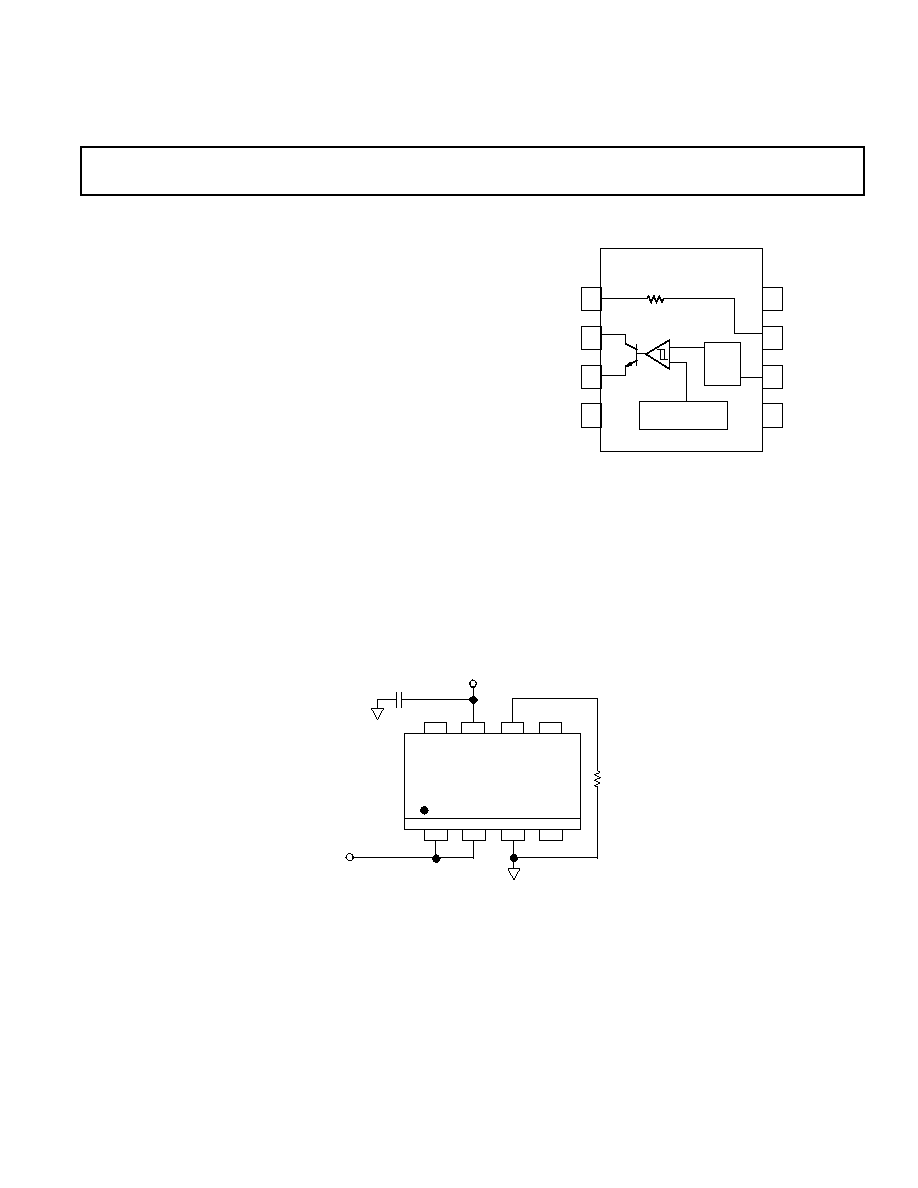
FUNCTIONAL BLOCK DIAGRAM
1
2
3
4
8
7
6
5
NC
V
S
R
SET
NC
R
PULL≠UP
OUT
GND
NC
TEMPERATURE
SENSOR
200k
SET≠
POINT
AD22105
1
2
3
4
8
7
6
5
OUT
+2.7V TO +7.0V
R
SET
AD22105
TOP VIEW
Figure 1. Typical Application Circuit
AD22105≠SPECIFICATIONS
Parameter
Symbol
Conditions
Min
Typ
Max
Units
TEMPERATURE ACCURACY
Ambient Setpoint Accuracy
ACC
±
0.5
±
2.0
∞
C
Temperature Setpoint Accuracy
ACC
T
≠40
∞
C
T
A
+125
∞
C
±
3.0
∞
C
Power Supply Rejection
PSR
+2.7 V
1
< V
S
< +7.0 V
±
0.05
±
0.15
∞
C/V
HYSTERESIS
Hysteresis Value
HYS
4.1
∞
C
OPEN COLLECTOR OUTPUT
Output Low Voltage
V
OL
I
SINK
= 5 mA
250
400
mV
POWER SUPPLY
Supply Range
V
S
+2.7
+7.0
V
Supply Current, Output "LOW"
IS
ON
120
µ
A
Supply Current, Output "HIGH"
IS
OFF
90
µ
A
INTERNAL PULL-UP RESISTOR
R
PULL-UP
140
200
260
k
TURN-ON SETTLING TIME
t
ON
5
µ
s
NOTES
1
The AD22105 will operate at voltages as low as +2.2 V.
Specifications subject to change without notice.
REV. 0
≠2≠
(V
S
= 3.3 V, T
A
= +25 C, R
LOAD
= internal 200 k
,
unless otherwise noted)
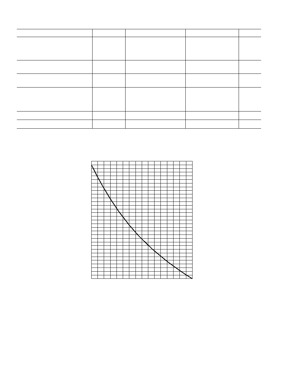
SET POINT TEMPERATURE ≠
∞
C
80
0
70
40
30
20
10
60
50
5
15
25
35
45
55
65
75
≠50
150
≠25
R
SET
- k
0
25
50
75
100
125
R
SET
= ≠≠≠≠≠≠≠≠≠≠≠≠------ ≠ 90.3k
39M
∞
C
T
SET
(
∞
C) + 281.6
∞
C
Figure 2. Setpoint Resistor Values
AD22105
REV. 0
≠3≠
ABSOLUTE MAXIMUM RATINGS*
Maximum Supply Voltage . . . . . . . . . . . . . . . . . . . . . . . +11 V
Maximum Output Voltage (Pin 2) . . . . . . . . . . . . . . . . +11 V
Maximum Output Current (Pin 2) . . . . . . . . . . . . . . . 10 mA
Operating Temperature Range . . . . . . . . . . ≠50
∞
C to +150
∞
C
Dice Junction Temperature . . . . . . . . . . . . . . . . . . . . +160
∞
C
Storage Temperature Range . . . . . . . . . . . . ≠65
∞
C to +160
∞
C
Lead Temperature (Soldering, 10 sec) . . . . . . . . . . . +300
∞
C
*Stresses above those listed under "Absolute Maximum Ratings" may cause
permanent damage to the device. This is a stress rating only and functional
operation of the device at these or any other conditions above those listed in the
operational sections of this specification is not implied. Exposure to absolute
maximum rating conditions for extended periods may affect device reliability.
ORDERING GUIDE
Package
Package
Model
Description
Option
AD22105AR
8-Lead SOIC
SO-8
AD22105AR-REEL7
8-Lead SOIC
SO-8
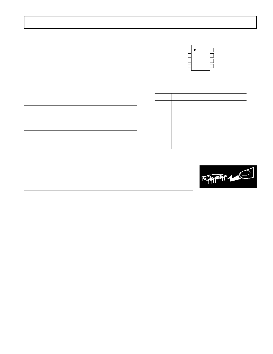
PIN CONFIGURATION
1
2
3
4
8
7
6
5
NC = NO CONNECT
AD22105
R
PULL-UP
NC
R
SET
V
S
NC
OUT
GND
NC
TOP VIEW
(Not to Scale)
PIN DESCRIPTION
Pin No.
Description
1
R
PULL-UP,
Internal 200 k
(Optional)
2
OUT
3
GND
4
No Connection
5
No Connection
6
R
SET
, Temperature Setpoint Resistor
7
V
S
8
No Connection
WARNING!
ESD SENSITIVE DEVICE
CAUTION
ESD (electrostatic discharge) sensitive device. Electrostatic charges as high as 4000 V readily
accumulate on the human body and test equipment and can discharge without detection.
Although the AD22105 features proprietary ESD protection circuitry, permanent damage may
occur on devices subjected to high energy electrostatic discharges. Therefore, proper ESD
precautions are recommended to avoid performance degradation or loss of functionality.

AD22105≠Typical Performance Characteristics
REV. 0
≠4≠
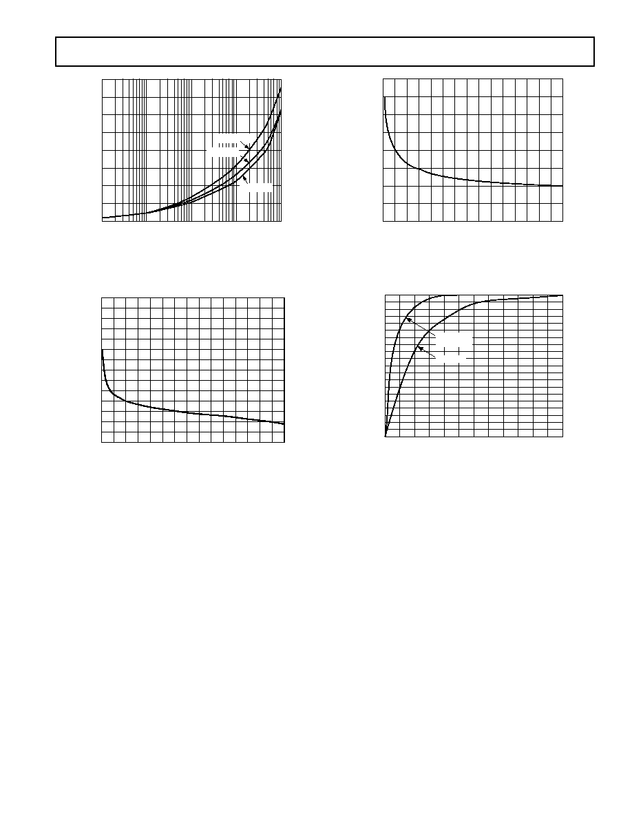
ERROR ≠
∞
C
TEMPERATURE ≠
∞
C
4
≠4
≠50
150
≠25
0
25
50
75
100
125
3
0
≠1
≠2
≠3
2
1
GUARANTEED LIMIT (+)
GUARANTEED LIMIT (≠)
Figure 3. Error vs. Setpoint
ERROR ≠
∞
C/%
TEMPERATURE ≠
∞
C
0.1
0.3
1.1
≠50
150
≠25
0
25
50
75
100
125
0.5
0.7
0.9
±
±
±
±
±
±
Figure 4. Setpoint Error Due to R
SET
Tolerance
I
S
≠ µA
TEMPERATURE ≠
∞
C
90
40
≠50
150
≠25
0
25
50
75
100
125
80
60
50
70
V
S
= 7V
V
S
= 5V
V
S
= 3V
Figure 5. Supply Current vs. Temperature (V
OUT
= HIGH)
HYSTERESIS ≠
∞
C
TEMPERATURE ≠
∞
C
4.4
3.2
≠50
150
≠25
0
25
50
75
100
125
4.2
4.0
3.8
3.6
3.4
Figure 6. Hysteresis vs. Setpoint
ERROR ≠
∞
C
V
S
2.0
1.5
≠2.0
3
7
4
5
6
0.0
≠0.5
≠1.0
≠1.5
1.0
0.5
+125
∞
C
+25
∞
C
≠40
∞
C
Figure 7. Setpoint Error vs. Supply Voltage
I
S
≠ µA
TEMPERATURE ≠
∞
C
120
60
≠50
150
≠25
0
25
50
75
100
125
110
100
90
80
70
V
S
= 7V
V
S
= 5V
V
S
= 3V
Figure 8. Supply Current vs. Temperature (V
OUT
= LOW)
AD22105
REV. 0
≠5≠
0.4
0.3
0.0
10µA
10mA
1mA
100µA
1µA
0.2
0.1
I
OUT
V
OUT
T
A
= +150
∞
C
T
A
= +25
∞
C
T
A
= ≠40
∞
C
Figure 9. V
OUT
vs. I
OUT
(V
OUT
= LOW)
≠ sec
FLOW RATE ≠ CFM
16
14
2
0
1200
400
800
10
8
6
4
12
Figure 10. Thermal Response vs. Flow Rate
FLOW RATE ≠ CFM
250
200
0
1200
JA
≠
∞
C/W
400
800
150
100
50
Figure 11. Thermal Resistance vs. Flow Rate
% OF FINAL VALUE
TIME ≠ sec
100
80
0
0
60
10
20
30
40
50
60
40
20
90
70
50
30
10
STILL AIR
MOVING AIR
(1200 CFM)
Figure 12. Thermal Response Time