Document Outline
- ˛ˇ
- ˛ˇ
- GENERAL DESCRIPTION
- ˛ˇ
- TABLE OF CONTENTS
- ˛ˇ
- ˛ˇ
- ˛ˇ
- ˛ˇ
- ˛ˇ
- ˛ˇ
- ˛ˇ

Dual-Axis, High-g,
iMEMS
Æ
Accelerometers
ADXL278
Rev. A
Information furnished by Analog Devices is believed to be accurate and reliable.
However, no responsibility is assumed by Analog Devices for its use, nor for any
infringements of patents or other rights of third parties that may result from its use.
Specifications subject to change without notice. No license is granted by implication
or otherwise under any patent or patent rights of Analog Devices. Trademarks and
registered trademarks are the property of their respective owners.
One Technology Way, P.O. Box 9106, Norwood, MA 02062-9106, U.S.A.
Tel: 781.329.4700
www.analog.com
Fax: 781.461.3113
©2005 Analog Devices, Inc. All rights reserved.
FEATURES
Complete dual-axis acceleration measurement system on
a single monolithic IC
Available in ±35 g/±35 g, ±50 g/±50 g, or ±70 g/±35 g
output full-scale ranges
Full differential sensor and circuitry for high resistance
to EMI/RFI
Environmentally robust packaging
Complete mechanical and electrical self-test on
digital command
Output ratiometric to supply
Sensitive axes in the plane of the chip
High linearity (0.2% of full scale)
Frequency response down to dc
Low noise
Low power consumption
Tight sensitivity tolerance and 0 g offset capability
Largest available prefilter clipping headroom
400 Hz, 2-pole Bessel filter
Single-supply operation
Compatible with Sn/Pb and Pb-free solder processes
APPLICATIONS
Vibration monitoring and control
Vehicle collision sensing
Shock detection
GENERAL DESCRIPTION
The ADXL278 is a low power, complete, dual-axis
accelerometer with signal conditioned voltage outputs that are
on a single monolithic IC. This product measures acceleration
with a full-scale range of (X-axis/Y-axis) ±35 g/±35 g, ±50 g/
±50 g, or ±70 g/±35 g (minimum). The ADXL278 can also
measure both dynamic acceleration (vibration) and static
acceleration (gravity).
The ADXL278 is the fourth-generation surface micromachined
iMEMSÆ accelerometer from ADI with enhanced performance
and lower cost. Designed for use in front and side impact airbag
applications, this product also provides a complete cost-
effective solution useful for a wide variety of other applications.
The ADXL278 is temperature stable and accurate over the
automotive temperature range, with a self-test feature that fully
exercises all the mechanical and electrical elements of the sensor
with a digital signal applied to a single pin.
The ADXL278 is available in a 5 mm ◊ 5 mm ◊ 2 mm,
8-terminal ceramic LCC package.
FUNCTIONAL BLOCK DIAGRAM
05365-001
ADXL278
V
DD
V
S
V
DD2
V
DD3
DIFFERENTIAL
SENSOR
EXC
DEMOD
AMP
Y
OUT
400Hz
BESSEL
FILTER
TIMING
GENERATOR
DIFFERENTIAL
SENSOR
EXC
DEMOD
AMP
X
OUT
400Hz
BESSEL
FILTER
SELF-TEST
Figure 1.

ADXL278
Rev. A | Page 2 of 12
TABLE OF CONTENTS
Specifications..................................................................................... 3
Absolute Maximum Ratings............................................................ 4
ESD Caution.................................................................................. 4
Pin Configuration and Function Descriptions............................. 5
Theory of Operation ........................................................................ 7
Applications....................................................................................... 8
Power Supply Decoupling ............................................................8
Self-Test ..........................................................................................8
Clock Frequency Supply Response .............................................8
Signal Distortion ...........................................................................8
Outline Dimensions ..........................................................................9
Ordering Guide .............................................................................9
REVISION HISTORY
5/05--Rev. 0 to Rev. A

ADXL278
Rev. A | Page 3 of 12
SPECIFICATIONS
1
At T
A
= -40∞C to +105∞C, 5.0 V dc ± 5%, acceleration = 0 g, unless otherwise noted.
Table 1.
Model No. AD22284
Model No. AD22285
Model No. AD22286
Parameter Conditions
Min
Typ
Max
Min Typ Max Axis Min Typ Max Unit
SENSOR
Output Full-Scale Range
I
OUT
±100 A
37
55
X
70
g
Y
37
g
Nonlinearity
0.2
2
0.2
2
0.2
2
%
Package Alignment Error
1
1
1
Degree
Sensor-to-Sensor
Alignment Error
0.1
0.1
0.1
Degree
Cross-Axis
Sensitivity
-5 +5 -5 +5 -5 +5 %
Resonant
Frequency
24
24
24
kHz
Sensitivity, Ratiometric
(Over Temperature)
V
DD
= 5 V,
100 Hz
52.25 55 57.75 36.1 38 39.9 X
25.65 27 28.35 mV/g
Y
52.25
55
57.75
mV/g
OFFSET
Zero-g Output Voltage
(Over Temperature)
2
V
OUT
- V
DD
/2,
V
DD
= 5 V
-150
+150 -150
+150 X
-100
+100 mV
Y
-150
+150
mV
NOISE
Noise Density
10 Hz - 400 Hz,
5 V
1.1
3
1.4
3
X
1.8
3.5
mg/Hz
Y
1.1
3
mg/Hz
Clock
Noise
5
5
5
mV
p-p
FREQUENCY RESPONSE
2-pole Bessel
-3 dB Frequency
360
400
440
360
400
440
360
400
440
Hz
-3 dB Frequency Drift
25∞C to
T
MIN
or T
MAX
2
2
2
Hz
SELF-TEST
Output Change
(Cube vs. V
DD
)
3
V
DD
= 5 V
440
550
660
304
380
456
X
216
270
324
mV
Y
440
550
660
mV
Logic Input High
V
DD
= 5 V
3.5
3.5
3.5
V
Logic Input Low
V
DD
= 5 V
1
1
1
V
Input Resistance
Pull-down
resistor to GND
30 50
30 50
30 50
k
OUTPUT
AMPLIFIER
Output Voltage Swing
I
OUT
= ±400 A
0.25
V
DD
-
0.25
0.25
V
DD
-
0.25
0.25
V
DD
-
0.25
V
Capacitive Load Drive
1000
1000
1000
pF
PREFILTER
HEADROOM
280
400
560
g
CFSR @ 400 kHz
6
4.5
3
V/V
6
V/V
POWER SUPPLY (V
DD
)
4.75
5.25 4.75
5.25
4.75
5.25 V
Functional Range
3.5
6
3.5
6
3.5
6
V
Quiescent Supply Current
V
DD
= 5 V
2.2
2.9
2.2
2.9
2.2
2.9
mA
TEMPERATURE RANGE
-40
+105
-40
+105
-40
+105
∞C
1
All minimum and maximum specifications are guaranteed. Typical specifications are not guaranteed.
2
Zero g output is ratiometric.
3
Self-test output at V
DD
= (Self-Test Output at 5 V) ◊ (V
DD
/5 V)
3
.

ADXL278
Rev. A | Page 4 of 12
ABSOLUTE MAXIMUM RATINGS
Table 2.
Parameter Rating
Acceleration (Any Axis, Unpowered)
4,000 g
Acceleration (Any Axis, Powered)
4,000 g
V
S
-0.3 V to +7.0 V
All Other Pins
(COM - 0.3 V) to
(V
S
+ 0.3 V)
Output Short-Circuit Duration
(Any Pin to Common)
Indefinite
Operating Temperature Range
-65∞C to +150∞C
Storage Temperature
-65∞C to +150∞C
Stresses above those listed under Absolute Maximum Ratings
may cause permanent damage to the device. This is a stress
rating only; functional operation of the device at these or any
other conditions above those indicated in the operational
section of this specification is not implied. Exposure to absolute
maximum rating conditions for extended periods may affect
device reliability.
ESD CAUTION
ESD (electrostatic discharge) sensitive device. Electrostatic charges as high as 4000 V readily accumulate on the
human body and test equipment and can discharge without detection. Although this product features
proprietary ESD protection circuitry, permanent damage may occur on devices subjected to high energy
electrostatic discharges. Therefore, proper ESD precautions are recommended to avoid performance
degradation or loss of functionality.

ADXL278
Rev. A | Page 5 of 12
PIN CONFIGURATION AND FUNCTION DESCRIPTIONS
05365-
002
NC = NO CONNECT
V
DD3
1
Y
OUT
2
COM
3
V
DD
7
X
OUT
6
NC
5
ST
TOP VIEW
(Not to Scale)
ADXL278
4
V
DD2
8
Figure 2. Pin Configuration
Table 3. Pin Function Descriptions
Pin No.
Mnemonic
Description
1 V
DD3
3.5 V to 6 V
2 Y
OUT
Y Channel Output
3 COM
Common
4 ST
Self-Test
5
NC
Do Not Connect
6 X
OUT
X Channel Output
7 V
DD
3.5 V to 6 V
8 V
DD2
3.5 V to 6 V

ADXL278
Rev. A | Page 6 of 12
05365-003
t
P
t
L
t
25∞C TO PEAK
t
S
PREHEAT
CRITICAL ZONE
T
L
TO T
P
TE
MP
E
RATURE
TIME
RAMP-DOWN
RAMP-UP
T
SMIN
T
SMAX
T
P
T
L
Figure 3. Recommended Soldering Profile
Table 4. Recommended Soldering Profile
Profile Feature
Sn63/Pb37
Pb-Free
AVERAGE RAMP RATE (T
L
TO T
P
)
3∞C/s max
3∞C/s max
PREHEAT
Minimum Temperature (T
SMIN
) 100∞C
150∞C
Maximum Temperature (T
SMAX
) 150∞C
200∞C
TIME (T
SMIN
TO T
SMAX
), t
S
60 s - 120 s
60 s - 150 s
T
SMAX
TO T
L
Ramp-Up Rate
3∞C/s
3∞C/s
TIME MAINTAINED ABOVE LIQUIDOUS (T
L
)
Liquidous Temperature (T
L
) 183∞C
217∞C
Time (t
L
)
60 s - 150 s
60 s - 150 s
PEAK TEMPERATURE (T
P
)
240∞C + 0∞C/-5∞C
260∞C + 0∞C/-5∞C
TIME WITHIN 5∞C OF ACTUAL PEAK TEMPERATURE (t
P
)
10 s - 30 s
20 s - 40 s
RAMP-DOWN RATE
6∞C/s max
6∞C/s max
TIME 25∞C TO PEAK TEMPERATURE
6 min max
8 min max
05365-004
EARTH'S SURFACE
XXXXX
XXXX
22285
PIN 8
Y
OUT
= 2.500V
X
OUT
= 2.462V
XXXXX
XXXX
22285
Y
OUT
= 2.462V
X
OUT
= 2.500V
XXXXX XXXX
22285
XXXXX
XXXX
22285
Y
OUT
= 2.538V
X
OUT
= 2.500V
Y
OUT
= 2.500V
X
OUT
= 2.538V
Y
OUT
= 2.500V
X
OUT
= 2.500V
Figure 4. Output Response vs. Orientation

ADXL278
Rev. A | Page 7 of 12
THEORY OF OPERATION
The ADXL278 provides a fully differential sensor structure and
circuit path, resulting in the industry's highest resistance to
EMI/RFI effects. This latest generation uses electrical feedback
with zero-force feedback for improved accuracy and stability.
The sensor resonant frequency is significantly higher than the
signal bandwidth set by the on-chip filter, avoiding the signal
analysis problems caused by resonant peaks near the signal
bandwidth.
Figure 5 is a simplified view of one of the differential sensor
elements. Each sensor includes several differential capacitor
unit cells. Each cell is composed of fixed plates attached
to the substrate and movable plates attached to the frame.
Displacement of the frame changes the differential capacitance,
which is measured by the on-chip circuitry.
Complementary 200 kHz square waves drive the fixed plates.
Electrical feedback adjusts the amplitudes of the square waves
such that the ac signal on the moving plates is 0. The feedback
signal is linearly proportional to the applied acceleration. This
unique feedback technique ensures that there is no net
electrostatic force applied to the sensor. The differential
feedback control signal is also applied to the input of the filter,
where it is filtered and converted to a single-ended signal.
05365-005
UNIT
SENSING
CELL
MOVABLE
FRAME
FIXED
PLATES
UNIT
FORCING
CELL
ANCHOR
MOVING
PLATE
PLATE
CAPACITORS
ACCE
LE
RATION
ANCHOR
Figure 5. Simplified View of Sensor Under Acceleration

ADXL278
Rev. A | Page 8 of 12
APPLICATIONS
POWER SUPPLY DECOUPLING
For most applications, a single 0.1 F capacitor, C
DC
, adequately
decouples the accelerometer from noise on the power supply.
However, in some cases, particularly where noise is present at
the 200 kHz internal clock frequency (or any harmonic
thereof), noise on the supply can cause interference on the
ADXL278's output. If additional decoupling is needed, a 50
(or smaller) resistor or ferrite bead cany be inserted in the
supply line. Additionally, a larger bulk bypass capacitor (in the
1 F to 4.7 F range) can be added in parallel to C
DC
.
SELF-TEST
The fixed fingers in the forcing cells are normally kept at the
same potential as that of the movable frame. When the self-test
digital input is activated, the voltage on the fixed fingers on one
side of the moving plate in the forcing cells is changed. This
creates an attractive electrostatic force, which causes the frame
to move towards those fixed fingers. The entire signal channel is
active; therefore, the sensor displacement causes a change in
V
OUT
. The ADXL278's self-test function is a comprehensive
method of verifying the operation of the accelerometer.
Because electrostatic force is independent of the polarity of the
voltage across capacitor plates, a positive voltage is applied in
half of the forcing cells, and its complement in the other half of
the forcing cells. Activating self-test causes a step function force
to be applied to the sensor, while the capacitive coupling term is
canceled. The ADXL278 has improved self-test functionality,
including excellent transient response and high speed switching
capabilities. Arbitrary force waveforms can be applied to the
sensor by modulating the self-test input, such as test signals to
measure the system frequency response or even crash signals to
verify algorithms within the limits of the self-test swing.
The ST pin should never be exposed to voltages greater than
V
S
+ 0.3 V. If this cannot be guaranteed due to the system
design (for instance, if there are multiple supply voltages), then
a low V
F
clamping diode between ST and V
S
is recommended.
CLOCK FREQUENCY SUPPLY RESPONSE
In any clocked system, power supply noise near the clock
frequency may have consequences at other frequencies. An
internal clock typically controls the sensor excitation and the
signal demodulator for micromachined accelerometers.
If the power supply contains high frequency spikes, they may be
demodulated and interpreted as an acceleration signal. A signal
appears as the difference between the noise frequency and the
demodulator frequency. If the power supply spikes are 100 Hz
away from the demodulator clock, there is an output term at
100 Hz. If the power supply clock is at exactly the same frequency
as the accelerometer clock, the term appears as an offset.
If the difference frequency is outside of the signal bandwidth,
the filter attenuates it. However, both the power supply clock
and the accelerometer clock may vary with time or temperature,
which can cause the interference signal to appear in the output
filter bandwidth.
The ADXL278 addresses this issue in two ways. First, the high
clock frequency eases the task of choosing a power supply clock
frequency such that the difference between it and the accelero-
meter clock remains well outside of the filter bandwidth.
Second, the ADXL278 is the only micromachined accelerometer
to have a fully differential signal path, including differential
sensors. The differential sensors eliminate most of the power
supply noise before it reaches the demodulator. Good high
frequency supply bypassing, such as a ceramic capacitor close to
the supply pins, also minimizes the amount of interference.
The clock frequency supply response (CFSR) is the ratio of the
response at V
OUT
to the noise on the power supply near the
accelerometer clock frequency. A CFSR of 3 means that the
signal at V
OUT
is 3◊ the amplitude of an excitation signal at V
DD
near the accelerometer internal clock frequency. This is
analogous to the power supply response, except that the
stimulus and the response are at different frequencies. The
ADXL278's CFSR is 10◊ better than a typical single-ended
accelerometer system.
SIGNAL DISTORTION
Signals from crashes and other events may contain high
amplitude, high frequency components. These components
contain very little useful information and are reduced by the
2-pole Bessel filter at the output of the accelerometer. However,
if the signal saturates at any point, the accelerometer output
does not look like a filtered version of the acceleration signal.
The signal may saturate anywhere before the filter. For example,
if the resonant frequency of the sensor is low, the displacement
per unit acceleration is high. The sensor may reach the
mechanical limit of travel if the applied acceleration is high
enough. This can be remedied by locating the accelerometer
where it does not see high values of acceleration and by using a
higher resonant frequency sensor, such as the ADXL278.
Also, the electronics may saturate in an overload condition
between the sensor output and the filter input. Ensuring that
internal circuit nodes operate linearly to at least several times
the full-scale acceleration value can minimize electrical
saturation. The ADXL278 circuit is linear to approximately 8◊
full scale.
ADXL278
Rev. A | Page 9 of 12
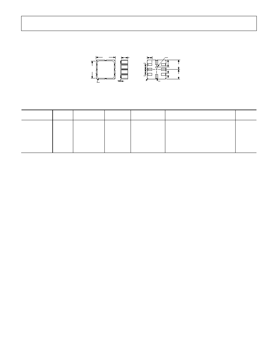
OUTLINE DIMENSIONS
BOTTOM VIEW
1
3
5
7
0.64
1.90
2.50
2.50
0.38 DIAMETER
0.50 DIAMETER
1.27
1.27
1.27
4.50
SQ
5.00
SQ
TOP VIEW
R 0.38
0.20
1.78
R 0.20
Figure 6. 8-Terminal Ceramic Leadless Chip Carrier [LCC]
(E-8)
Dimensions shown in millimeters
AXL278 ORDERING GUIDE
Model
1
Parts
per Reel
Measurement
Range
Specified
Voltage (V)
Temperature
Range Package
Description
Package
Option
AD22284-A-R2 250
±35
g/±35 g
5
-40∞C to +105∞C
8-Lead Ceramic Leadless Chip Carrier
E-8
AD22284-A 3000 ±35
g/±35 g
5
-40∞C to +105∞C
8-Lead Ceramic Leadless Chip Carrier
E-8
AD22285-R2 250
±50
g/±50 g
5
-40∞C to +105∞C
8-Lead Ceramic Leadless Chip Carrier
E-8
AD22285 3000
±50
g/±50 g
5
-40∞C to +105∞C
8-Lead Ceramic Leadless Chip Carrier
E-8
AD22286-R2 250
±70
g/±35 g
5
-40∞C to +105∞C
8-Lead Ceramic Leadless Chip Carrier
E-8
AD22286 3000
±70
g/±35 g
5
-40∞C to +105∞C
8-Lead Ceramic Leadless Chip Carrier
E-8
1
All models are on tape and reel and are Pb-free parts.

ADXL278
Rev. A | Page 10 of 12
NOTES

ADXL278
Rev. A | Page 11 of 12
NOTES

ADXL278
Rev. A | Page 12 of 12
NOTES
©2005 Analog Devices, Inc. All rights reserved. Trademarks and
registered trademarks are the property of their respective owners.
D05365≠0≠5/05(A)