 | ÐлекÑÑоннÑй компоненÑ: AD260 | СкаÑаÑÑ:  PDF PDF  ZIP ZIP |
Äîêóìåíòàöèÿ è îïèñàíèÿ www.docs.chipfind.ru
REV. 0
Information furnished by Analog Devices is believed to be accurate and
reliable. However, no responsibility is assumed by Analog Devices for its
use, nor for any infringements of patents or other rights of third parties
which may result from its use. No license is granted by implication or
otherwise under any patent or patent rights of Analog Devices.
a
AD260
One Technology Way, P.O. Box 9106, Norwood, MA 02062-9106, U.S.A.
Tel: 781/329-4700
World Wide Web Site: http://www.analog.com
Fax: 781/326-8703
© Analog Devices, Inc., 1998
High Speed, Logic Isolator
with Power Transformer
FUNCTIONAL BLOCK DIAGRAM
S0
1
F3
21
SYSTEM
FIELD
+5Vdc
5Vdc RTN
DRIVE
+5Vdc
5Vdc RTN
17V p-p OUT
CT OUT
17V p-p OUT
S1
2
S2
3
S3
S4
DRVA
F0
F1
F2
F4
19
20
22
15
16
18
6
7
8
4
5
AD260
+5V
DRVCT
DRIVE
DRVB
TRISTATE
LATCH
E
D
LINE 2
TRISTATE
LATCH
E
D
LINE 1
TRISTATE
LATCH
E
TRISTATE
D
LINE 0
13
14
9
12
10
11
LATCH
D
E
LINE 4
TRISTATE
LATCH
D
E
LINE 3
TRISTATE
+5Vdc
FLD
5V RTN
FLD
ENABLE
FLD
PWRA
FLD
PWRCT
FLD
PWRB
FLD
5V RTN
SYS
+5Vdc
SYS
ENABLE
SYS
17
FEATURES
IsoLogicTM Circuit Architecture
Isolation Test Voltage: To 3.5 kV rms
Five Isolated Logic Lines: Available in Six I/O Configurations
Logic Signal Bandwidth: 20 MHz (Min), 40 mbps (NRZ)
Isolated Power Transformer: 37 V p-p, 1.5 W Max
CMV Transient Immunity: 10 kV/ s Min
Waveform Edge Transmission Symmetry: 1 ns
Field and System Output Enable/Three-State Functions
Performance Rated Over 25 C to +85 C
UL1950, IEC950, EN60950 Certification, Pending
APPLICATIONS
PLC/DCS Analog Input and Output Cards
Communications Bus Isolation
General Data Acquisition Applications
IGBT Motor Drive Controls
High Speed Digital I/O Ports
GENERAL DESCRIPTION
The AD260 is designed using Analog Devices new IsoLogic
circuit architecture to isolate five digital control signals to/
from a microcontroller and its related field I/O components. Six
models allow all I/O combinations from five input lines to five
output lines, including combinations in between. Every AD260
effectively replaces up to five opto-isolators while also providing
the 1.5 W transformer for a 3.5 kV isolated dc-dc power supply
circuit.
Each line of the AD260 has a bandwidth of 20 MHz (min) with
a propagation delay of only 14 ns, which allows for extremely
fast data transmission. Output waveform symmetry is maintained
to within
±
1 ns of the input so the AD260 can be used to accu-
rately isolate time-based PWM signals.
All field or system output pins of the AD260 can be set to a high
resistance three-state level by use of the two enable pins. A field
output three-stated offers a convenient method of presetting
logic levels at power-up by use of pull-up/down resistors. Sys-
tem side outputs being three-stated allows for easy multiplexing
of multiple AD260s.
The isolation barrier of the AD260 B Grade is 100% tested at
3.5 kV rms (system to field). The barrier design also provides
excellent common-mode transient immunity from 10 kV/
µ
s
common-mode voltage excursions of field side terminals relative
to the system side, with no false output triggering on either side.
Each output is updated within nanoseconds by input logic tran-
sitions, the AD260 also has a continuous output update feature
that automatically updates each output based on the dc level of
the input. This guarantees the output is always valid 10
µ
s after
a fault condition or after the power-up reset interval.
The AD260 also has an integral center tap transformer for gen-
erating isolated power. Typically driven by a 5 V push-pull drive
at the primary, it will generate a 37 V p-p output capable of
supplying up to 1.5 W. This can then be regulated to the de-
sired voltage, including
±
5 V dc for circuit components and
24 V for a 20 mA loop supply when needed.
PRODUCT HIGHLIGHTS
Six Isolated Logic Line I/O Configurations Available: The
AD260 is available in six pin-compatible versions of I/O con-
figurations to meet a wide variety of requirements
.
Wide Bandwidth with Minimal Edge Error: The AD260 with
IsoLogic affords extremely fast isolation of logic signals due to its
20 MHz bandwidth and 14 ns propagation delay. It maintains a
waveform input-to-output edge transition error of typically less
than
±
1 ns (total) for positive vs. negative transition.
3.5 kV rms Test Voltage Isolation Rating: The AD260
B Grade is rated to operate at 1.25 kV rms and is 100% pro-
duction tested at 3.5 kV rms, using a standard ADI test method.
High Transient Immunity: The AD260 rejects common-
mode transients slewing at up to 10 kV/
µ
s without false trigger-
ing or damage to the device.
(Continued on page 6)
IsoLogic is a trademark of Analog Devices, Inc.

2
REV. 0
AD260SPECIFICATIONS
(Typical at T
A
= +25 C, +5 V dc
SYS
, +5 V dc
FLD
, t
RR
= 50 ns max unless otherwise noted)
Parameter
Conditions
Min
Typ
Max
Units
INPUT CHARACTERISTICS
Threshold Voltage
Positive Transition (V
T+
)
+5 V dc
SYS
= 4.5 V
2.0
2.7
3.15
V
+5 V dc
SYS
= 5.5 V
3.0
3.2
4.2
V
Negative Transition (V
T
)
+5 V dc
SYS
= 4.5 V
0.9
1.8
2.2
V
+5 V dc
SYS
= 5.5 V
1.2
2.2
3.0
V
Hysteresis Voltage (V
H
)
+5 V dc
SYS
= 4.5 V
0.4
0.9
1.4
V
+5 V dc
SYS
= 5.5 V
0.5
1.0
1.5
V
Input Capacitance (C
IN
)
5
pF
Input Bias Current (I
IN
)
Per Input
0.5
µ
A
OUTPUT CHARACTERISTICS
Output Voltage
1
High Level (V
OH
)
+5 V dc
SYS
= 4.5 V, |I
O
| = 0.02 mA
4.4
V
+5 V dc
SYS
= 4.5 V, |I
O
| = 4 mA
3.7
V
Low Level (V
OL
)
+5 V dc
SYS
= 4.5 V, |I
O
| = 0.02 mA
0.1
V
+5 V dc
SYS
= 4.5 V, |I
O
| = 4 mA
0.4
V
Output Three-State Leakage Current
ENABLE
SYS/FLD
@ Logic Low/High Level Respectively
0.5
µ
A
DYNAMIC RESPONSE
1
(Refer to Figure 2)
Max Logic Signal Frequency (f
MIN
)
50% Duty Cycle, +5 V dc
SYS
= 5 V
20
MHz
Waveform Edge Symmetry Error (t
ERROR
)
t
PHL
vs. t
PLH
±
1
ns
Logic Edge Propagation Delay (t
PHL
, t
PLH
)
14
25
ns
Minimum Pulsewidth (t
PWMIN
)
25
ns
Max Output Update Delay on Fault or After
Power-Up Reset Interval (
30
µ
s
)
2
12
µ
s
ISOLATION BARRIER RATING
3
Operating Isolation Voltage (V
CMV
)
AD260A
375
V rms
AD260B
1250
V rms
Isolation Rating Test Voltage (V
CMV TEST
)
4
AD260A
1750
V rms
AD260B
3500
V rms
Transient Immunity (V
TRANSIENT
)
10,000
V/
µ
s
Isolation Mode Capacitance (C
ISO
)
Total Capacitance, All Lines and Transformer
14
18
pF
Capacitive Leakage Current (I
LEAD
)
240 V rms @ 60 Hz
2
µ
A rms
POWER TRANSFORMER
Primary Winding
Bifilar Wound, Center-Tapped
Inductance (LP)
Each Half
1
mH
Number of Turns (NP)
Each Half
26
Turns
Resistance
Each Half
0.6
Max Volt-Seconds (E
×
t)
Each Half
27
V
×
µ
s
Recommended Operating Frequency
25
°
C to +85
°
C, Push-Pull Drive
150
200
300
kHz
Absolute Min Operating Frequency
25
°
C to +85
°
C, Push-Pull Drive
75
kHz
Secondary Winding
Bifilar Wound, Center-Tapped
Number of Turns (NS)
Each Half
48
Turns
Resistance
Each Half
2.3
Insulation Withstand (V
CMV TEST
)
Primary to Secondary
3,500
V rms
Capacitance
Primary to Secondary
5
pF
Recommended Max Power
Rated Performance
1.0
1.5
W
POWER SUPPLY
Supply Voltage (+5 V dc
SYS
and +5 V dc
FLD
)
Rated Performance
4.5
5.5
V dc
Operating
4.0
5.75
V dc
Power Dissipation Capacitance
Effective, per Input, Either Side
8
pF
Effective per Output, Either Side--No Load
28
pF
Quiescent Supply Current
Each, +5 V dc
SYS & FLD
4
mA
Supply Current
All Lines @ 10 MHz (Sum of +5 V dc
SYS & FLD
)
18
mA
TEMPERATURE RANGE
Rated Performance (T
A
)
5
25
+85
°
C
Storage (T
STG
)
40
+85
°
C
NOTES
1
For best performance, bypass +5 V dc supplies to com. at or near the device (0.01
µ
F). +5 V dc supplies are also internally bypassed with 0.05
µ
F.
2
As the supply voltage is applied to either side of the AD260, the internal circuitry will go into a power-up reset mode (all lines disabled) for about 30
µ
s after the point where
+5 V dc
SYS & FLD
passes above 3.3 V.
3
"Operating" isolation voltage is derived from the Isolation Test Voltage in accordance with such methods as found in VDE-0883 wherein a device will be "hi-pot" tested at twice
the operating voltage, plus one thousand volts. Partial discharge testing, with an acceptance threshold of 80 pC of discharge may be considered the same as a hi-pot test (but
nondestructive).
4
Partial Discharge at 80 pC THLD.
5
Supply Current will increase slightly, but otherwise the unit will function within specification to 40
°
C.
Specifications are subject to change without notice.
AD260
3
REV. 0
WARNING!
ESD SENSITIVE DEVICE
CAUTION
ESD (electrostatic discharge) sensitive device. Electrostatic charges as high as 4000 V readily
accumulate on the human body and test equipment and can discharge without detection.
Although the AD260 features proprietary ESD protection circuitry, permanent damage may
occur on devices subjected to high energy electrostatic discharges. Therefore, proper ESD
precautions are recommended to avoid performance degradation or loss of functionality.
ABSOLUTE MAXIMUM RATINGS*
Parameter
Conditions
Min
Typ
Max
Units
Supply Voltage (+5 V dc
SYS & FLD
)
0.5
+6.0
V
DC Input Voltage (V
IN MAX
)
Referred to +5 V dc
SYS & FLD
and 5 V RTN
SYS & FLD
Respectively
0.5
+0.5
V
DC Output Voltage (V
OUT MAX
)
Referred to +5 V RTN
SYS & FLD
and 5 V dc
SYS & FLD
Respectively
0.5
+0.5
V
Clamp Diode Input Current (I
IK
)
For V
I
< 0.5 V or V
I
> 5 V RTN
SYS & FLD
+0.5 V
25
+25
mA
Clamp Diode Output Current (I
OK
)
For V
O
< 0.5 V or V
O
> 5 V RTN
SYS & FLD
+0.5 V
25
+25
mA
Output DC Current, per Pin (I
OUT
)
25
+25
mA
DC Current, V
CC
or GND (I
CC
or I
GND
)
50
+50
mA
Storage Temperature (T
STG
)
40
+85
°
C
Lead Temperature (Soldering, 10 sec)
+300
°
C
Electrostatic Protection (V
ESD
)
Per MIL-STD-883, Method 3015
4.5
5
kV
*Stresses above those listed under Absolute Maximum Ratings may cause permanent damage to the device. This is a stress rating only; functional operation of the device
at these or any other conditions above those indicated in the operational sections of this specification is not implied. Exposure to absolute maximum ratings for extended
periods may effect device reliability.
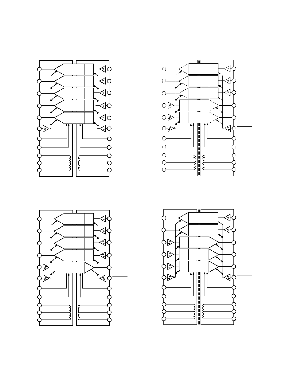
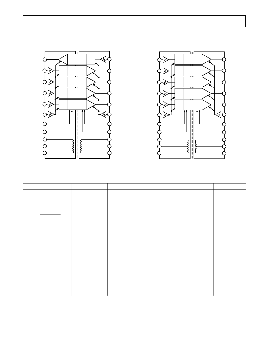
I/O CONFIGURATIONS AVAILABLE
The AD260 is available in several configurations. The choice of
model is determined by the desired number of input vs. output
lines. All models have identical footprints with the power and
enable pins always being in the same locations.
PIN CONFIGURATION
12
13
14
15
16
17
18
19
20
21
22
1
2
3
4
5
6
7
8
9
10
11
SYSTEM
FIELD
BOTTOM VIEW
S0
S1
S2
S3
S4
ENABLE
SYS
+5Vdc
SYS
5V RTN
SYS
DRVA
DRVCT
DRVB
PWRB
FLD
PWRCT
FLD
PWRA
FLD
5V RTN
FLD
+5Vdc
FLD
ENABLE
FLD
F0
F1
F2
F3
F4
ORDERING GUIDE
Model Number
Description
Isolation Test Voltage
Package Description
Package Option
AD260AND-0
0 Inputs, 5 Outputs
1.75 kV rms
Plastic DIP
ND-22
AD260AND-1
1 Input, 4 Outputs
1.75 kV rms
Plastic DIP
ND-22
AD260AND-2
2 Inputs, 3 Outputs
1.75 kV rms
Plastic DIP
ND-22
AD260AND-3
3 Inputs, 2 Outputs
1.75 kV rms
Plastic DIP
ND-22
AD260AND-4
4 Inputs, 1 Output
1.75 kV rms
Plastic DIP
ND-22
AD260AND-5
5 Inputs, 0 Outputs
1.75 kV rms
Plastic DIP
ND-22
AD260BND-0
0 Inputs, 5 Outputs
3.5 kV rms
Plastic DIP
ND-22
AD260BND-1
1 Input, 4 Outputs
3.5 kV rms
Plastic DIP
ND-22
AD260BND-2
2 Inputs, 3 Outputs
3.5 kV rms
Plastic DIP
ND-22
AD260BND-3
3 Inputs, 2 Outputs
3.5 kV rms
Plastic DIP
ND-22
AD260BND-4
4 Inputs, 1 Output
3.5 kV rms
Plastic DIP
ND-22
AD260BND-5
5 Inputs, 0 Outputs
3.5 kV rms
Plastic DIP
ND-22
PIN FUNCTION DESCRIPTIONS
Pin
Mnemonic
Function
15*
S0 Through S4 Digital Xmt or Rcv from F0 Through F4
6
ENABLE
SYS
System Output Enable /Three-State
7
+5 V dc
SYS
System Power Supply (+5 V dc Input)
8
5 V RTN
SYS
System Power Supply Common
914
Not Present On Unit
15
5 V RTN
FLD
Field Power Supply Common
16
+5 V dc
FLD
Field Power Supply (+5 V Input)
17
ENABLE
FLD
Field Output Enable/Three-State
1822* F0 Through F4 Digital Xmt or Rcv from S0 Through S4
*Function of pin determined by model. Refer to Table I.
Caution
: Use care in handling unit as contaminants on the bot-
tom side of the unit or the circuit card to which it is mounted will
lead to reduced breakdown voltage across the isolation barrier.
AD260
4
REV. 0
AD260BND-0
S0
1
F3
21
SYSTEM
FIELD
+5Vdc
5Vdc RTN
DRIVE
+5Vdc
5Vdc RTN
17V p-p OUT
CT OUT
17V p-p OUT
S1
2
S2
3
S3
S4
DRVA
F0
F1
F2
F4
19
20
22
15
16
18
6
7
8
4
5
AD260-0
+5V
DRVCT
DRIVE
DRVB
TR
IST
ATE
LATCH
E
D
LINE 2 OUT
TR
IST
ATE
LATCH
E
D
LINE 1 OUT
TR
IS
TA
TE
LATCH
E
TR
IST
ATE
D
LINE 0 OUT
13
14
9
12
10
11
+5Vdc
FLD
5V RTN
FLD
ENABLE
FLD
PWRA
FLD
PWRCT
FLD
PWRB
FLD
5V RTN
SYS
+5Vdc
SYS
ENABLE
SYS
17
TR
IST
ATE
LATCH
E
D
LINE 4 OUT
TR
IST
ATE
LATCH
E
D
LINE 3 OUT
AD260BND-1
S0
1
F3
21
SYSTEM
FIELD
+5Vdc
5Vdc RTN
DRIVE
+5Vdc
5Vdc RTN
17V p-p OUT
CT OUT
17V p-p OUT
S1
2
S2
3
S3
S4
DRVA
F0
F1
F2
F4
19
20
22
15
16
18
6
7
8
4
5
AD260-1
+5V
DRVCT
DRIVE
DRVB
TRISTATE
LATCH
E
D
TRISTATE
LATCH
E
D
TRISTATE
LATCH
E
TRISTATE
D
LINE 0 OUT
13
14
9
12
10
11
LATCH
D
E
TRISTATE
+5Vdc
FLD
5V RTN
FLD
ENABLE
FLD
PWRA
FLD
PWRCT
FLD
PWRB
FLD
5V RTN
SYS
+5Vdc
SYS
ENABLE
SYS
17
TRISTATE
LATCH
E
D
LINE 1 OUT
LINE 2 OUT
LINE 3 OUT
LINE 4 IN
PIN CONFIGURATIONS
AD260BND-2
S0
1
F3
21
SYSTEM
FIELD
+5Vdc
5Vdc RTN
DRIVE
+5Vdc
5Vdc RTN
17V p-p OUT
CT OUT
17V p-p OUT
S1
2
S2
3
S3
S4
DRVA
F0
F1
F2
F4
19
20
22
15
16
18
6
7
8
4
5
AD260-2
+5V
DRVCT
DRIVE
DRVB
TR
ISTATE
LATCH
E
D
LINE 2 OUT
TR
ISTA
TE
LATCH
E
D
LINE 1 OUT
TRIS
TATE
LATCH
E
TRISTA
TE
D
LINE 0 OUT
13
14
9
12
10
11
LATCH
D
E
LINE 4 IN
TRISTA
TE
LATCH
D
E
LINE 3 IN
TR
ISTATE
+5Vdc
FLD
5V RTN
FLD
ENABLE
FLD
PWRA
FLD
PWRCT
FLD
PWRB
FLD
5V RTN
SYS
+5Vdc
SYS
ENABLE
SYS
17
AD260BND-3
S0
1
F3
21
SYSTEM
FIELD
+5Vdc
5Vdc RTN
DRIVE
+5Vdc
5Vdc RTN
17V p-p OUT
CT OUT
17V p-p OUT
S1
2
S2
S3
S4
DRVA
F0
F1
F2
F4
19
20
22
15
16
18
6
7
8
4
5
AD260-3
+5V
DRVCT
DRIVE
DRVB
TRISTATE
LATCH
E
D
TRISTATE
LATCH
E
TRISTATE
D
LINE 0 OUT
13
14
9
12
10
11
LATCH
D
E
TRISTATE
LATCH
D
E
TRISTATE
+5Vdc
FLD
5V RTN
FLD
ENABLE
FLD
PWRA
FLD
PWRCT
FLD
PWRB
FLD
5V RTN
SYS
+5Vdc
SYS
ENABLE
SYS
17
3
LATCH
D
E
TRISTATE
LINE 1 OUT
LINE 2 IN
LINE 3 IN
LINE 4 IN
AD260
5
REV. 0
PIN CONFIGURATIONS
Table I.
Pin
AD260BND-0
AD260BND-1
AD260BND-2
AD260BND-3
AD260BND-4
AD260BND-5
1
S0 (Xmt)
S0 (Xmt)
S0 (Xmt)
S0 (Xmt)
S0 (Xmt)
S0 (Rcv)
2
S1 (Xmt)
S1 (Xmt)
S1 (Xmt)
S1 (Xmt)
S1 (Rcv)
S1 (Rcv)
3
S2 (Xmt)
S2 (Xmt)
S2 (Xmt)
S2 (Rcv)
S2 (Rcv)
S2 (Rcv)
4
S3 (Xmt)
S3 (Xmt)
S3 (Rcv)
S3 (Rcv)
S3 (Rcv)
S3 (Rcv)
5
S4 (Xmt)
S4 (Rcv)
S4 (Rcv)
S4 (Rcv)
S4 (Rcv)
S4 (Rcv)
6
ENABLE
SYS
*
*
*
*
*
7
+5 V dc
SYS
*
*
*
*
*
8
5 V RTN
SYS
*
*
*
*
*
9
DRVA
*
*
*
*
*
10
DRVCT
*
*
*
*
*
11
DRVB
*
*
*
*
*
12
PWRB
FLD
*
*
*
*
*
13
PWRCT
FLD
*
*
*
*
*
14
PWRA
FLD
*
*
*
*
*
15
5 V RTN
FLD
*
*
*
*
*
16
+5 V dc
FLD
*
*
*
*
*
17
ENABLE
FLD
*
*
*
*
*
18
F0 (Rcv)
F0 (Rcv)
F0 (Rcv)
F0 (Rcv)
F0 (Rcv)
F0 (Xmt)
19
F1 (Rcv)
F1 (Rcv)
F1 (Rcv)
F1 (Rcv)
F1 (Xmt)
F1 (Xmt)
20
F2 (Rcv)
F2 (Rcv)
F2 (Rcv)
F2 (Xmt)
F2 (Xmt)
F2 (Xmt)
21
F3 (Rcv)
F3 (Rcv)
F3 (Xmt)
F3 (Xmt)
F3 (Xmt)
F3 (Xmt)
22
F4 (Rcv)
F4 (Xmt)
F4 (Xmt)
F4 (Xmt)
F4 (Xmt)
F4 (Xmt)
*Pin function is the same on all models, as shown in the AD260BND-0 column.
AD260BND-4
S0
1
F3
21
SYSTEM
FIELD
+5Vdc
5Vdc RTN
DRIVE
+5Vdc
5Vdc RTN
17V p-p OUT
CT OUT
17V p-p OUT
S1
2
S2
3
S3
S4
DRVA
F0
F1
F2
F4
19
20
22
15
16
18
6
7
8
4
5
AD260-4
+5V
DRVCT
DRIVE
DRVB
TR
IS
TA
TE
LATCH
E
TR
IST
ATE
D
LINE 0 OUT
13
14
9
12
10
11
LATCH
D
E
TR
IST
AT
E
LATCH
D
E
TR
IST
AT
E
+5Vdc
FLD
5V RTN
FLD
ENABLE
FLD
PWRA
FLD
PWRCT
FLD
PWRB
FLD
5V RTN
SYS
+5Vdc
SYS
ENABLE
SYS
17
LATCH
D
E
TR
IST
AT
E
LATCH
D
E
TR
IST
AT
E
LINE 1 IN
LINE 2 IN
LINE 3 IN
LINE 4 IN
AD260BND-5
S0
1
F3
21
SYSTEM
FIELD
+5Vdc
5Vdc RTN
DRIVE
+5Vdc
5Vdc RTN
17V p-p OUT
CT OUT
17V p-p OUT
S1
S2
S3
S4
DRVA
F0
F1
F2
F4
19
20
22
15
16
18
6
7
8
4
5
AD260-5
+5V
DRVCT
DRIVE
DRVB
13
14
9
12
10
11
LATCH
D
E
TRISTATE
LATCH
D
E
TRISTATE
+5Vdc
FLD
5V RTN
FLD
ENABLE
FLD
PWRA
FLD
PWRCT
FLD
PWRB
FLD
5V RTN
SYS
+5Vdc
SYS
ENABLE
SYS
17
3
2
LATCH
D
E
TRISTATE
LATCH
D
E
TRISTATE
LATCH
D
E
LINE 0 IN
TRISTATE
LINE 1 IN
LINE 2 IN
LINE 3 IN
LINE 4 IN
AD260
6
REV. 0
t
f f
37%
63%
OUTPUT
INPUT
POSITIVE GOING
INPUT THRESHOLD
NEGATIVE GOING
INPUT THRESHOLD
HYSTERESIS
t
PD
t
PLH
t
PD
t
PHL
+3V
+2V
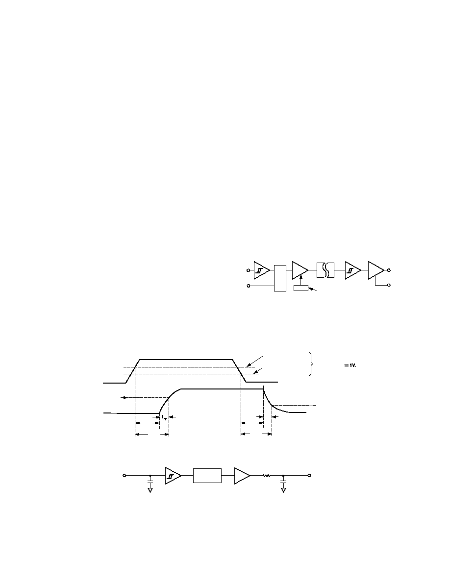
PROPAGATION DELAY
BUFFER
DELAY LINE
SCHMITT
TRIGGER
12.5ns
t
PD
100
5pF
OUTPUT
CAPACITANCE
t
rr
=
t
f f
= 100 x C
TOTAL OUTPUT CAPACITANCE
0.5ns NO LOAD
= 5.5ns INTO 50pF
5pF
INPUT
CAPACITANCE
TOTAL DELAY = (
t
PLH
OR
t
PHL
) =
t
PD
+ (
t
rr
OR
t
ff
)
13ns (NO LOAD), 18ns (50pF LOAD)
EFFECTIVE CIRCUIT MODEL FOR ONE ISOLATED LOGIC LINE
Figure 2. Typical Timing and Delay Models
(Continued from page 1)
Integral Isolated Power: The AD260 includes an integral,
uncommitted and flexible 1 Watt power transformer for devel-
oping isolated field power sources.
Field and System Enable Functions: Both the isolated and
nonisolated sides of the AD260 have ENABLE pins that three-
state all outputs. Upon reenabling these pins, all outputs are
updated to reflect the current input logic level.
CE Certifiable: Simply by adding the external bypass capacitors
at the supply pins, the AD260 can attain CE certification in
most applications (to the EMC directive) and conformance to
the low voltage (safety) directive is assured by the EN60950
certification.
GENERAL ATTRIBUTES
The AD260 provides five HCMOS/ACMOS compatible isolated
logic lines with
10 kV/
µ
s common-mode transient immunity.
The case design and pin arrangement provides greater than
18 mm spacing between field and system side conductors, pro-
viding CSA/IS and IEC creepage spacing consistent with 750 V
mains isolation.
The five unidirectional logic lines have six possible combina-
tions of "ins" and "outs," or transmitter/receiver pairs; hence
there are six AD260 part configurations (see Table I).
Each 20 MHz logic line
has a Schmidt trigger input and a three-
state output (on the other side of the isolation barrier) and 14 ns of
propagation delay. A single enable pin on either side of the
barrier causes all outputs on that side to go three-state and all
inputs (driven pins) to ignore their inputs and retain their last
known state.
Note: All unused logic inputs (15) should be tied either high or low,
but not left floating.
Edge "fidelity," or the difference in propagation time for rising
and falling edges, is typically less than
±
1 ns.
Power consumption, unlike opto-isolators, is a function of operat-
ing frequency. Each logic line barrier driver requires about 160
µ
A
per MHz and each receiver 40
µ
A per MHz plus, of course, 4 mA
total idle current (each side). The supply current diminishes
slightly with increasing temperature (about 0.03%/
°
C).
The total capacitance spanning the isolation barrier is less than
10 pF.
The minimum width of a pulse that can be accurately coupled
across the barrier is about 25 ns. Therefore the maximum
square-wave frequency of operation is 20 MHz.
Logic information is sent across the barrier as "set-hi/set-lo"
data that is derived from logic level transitions of the input. At
power-up or after a fault condition, an output might not repre-
sent the state of the respective channel input to the isolator. An
internal circuit operates in the background which interrogates all
inputs about every 5
µ
s and in the absence of logic transitions,
sends appropriate "set-hi" or "set-lo" data across the barrier.
Recovery time from a fault condition or at power-up is thus
between 5
µ
s and 10
µ
s.
DATA
RECEIVER
OUTPUT
BUFFER
GATED
TRANSPARENT
LATCH
SCHMITT
TRIGGER
CONTINUOUS
UPDATE CIRCUIT
3.5kV
ISOLATION
BARRIER
DATA IN
ENABLE
ENABLE
OUT
D
G
DATA
TRANSMITTER
Q
Figure 1. Simplified Block Diagram
AD260
7
REV. 0
The power transformer is designed to operate between 150 kHz
and 250 kHz and will easily deliver more than 1 W of isolated
power when driven push-pull (5 V) on the system side. Different
transformer tap, rectifier and regulator schemes will provide
combinations of
±
5 V, 15 V, 24 V or even 30 V or higher.
The output voltage when driven with a low voltage-drop drive
(@ 5 V push-pull) will be 37 V p-p across the entire secondary.
This will drop to 33 V p-p at 4.5 V drive.
3.3 F
TANT.
+
52T
CT
LM2524
12
11
14
13
COMP V
IN
V
REF
4.7k
9
15
16
3.3k
0.1 F
10
1
2
4
5
6
7
470pF
GND
INV
NI
C
L
+
C
T
R
T
C
L
LOGIC/SHUTDOWN (H
I
)
+5Vdc
8
3.3 F
TANT.
+
52T
CT
MAX
253
1
8
4
3
G
2
F
S
SHUTDOWN (
ON
/OFF)
+5Vdc
7
G
1
2
6
D
1
D
2
S
D
Figure 3. System Side Transformer Driver Examples
Application Examples
The following is an example of a typical transformer system-side
drive circuit and a field-side regulation circuit suitable for use in
most general applications.
+5V
REG
96T
CT.
5V ISO
+5V ISO
I
V
DD
FLD
ENABLE FLD
(PWR-UP ENABLE)
5V
REG
Figure 4.
a
a
+5Vdc/+4.5Vdc
150mA
+
LOAD
COM
80mA
b
COM
20mA
b
+
20mA
b
+5Vdc/+4.5Vdc
150mA
COM
20mA
b
+
20mA
a
+5Vdc/+4.5Vdc
150mA
COM
40mA
a
+
40mA
a
a
7.72
7.62
15.79
23.5
7.72
a
+5Vdc/+4.5Vdc
150mA
COM
20mA
b
+
20mA
b
+
V
OUT
@
5V DRIVE
V(MIN) @
4.5V DRIVE
+8.55
17.63
8.64
+26.3
+8.64
"a" DIODES IN5818/MBR0530
"b" DIODES IN5819/MBR0540
Figure 5. Field Side Power Supply Rectifier Examples
AD260
8
REV. 0
C303189/98
PRINTED IN U.S.A.
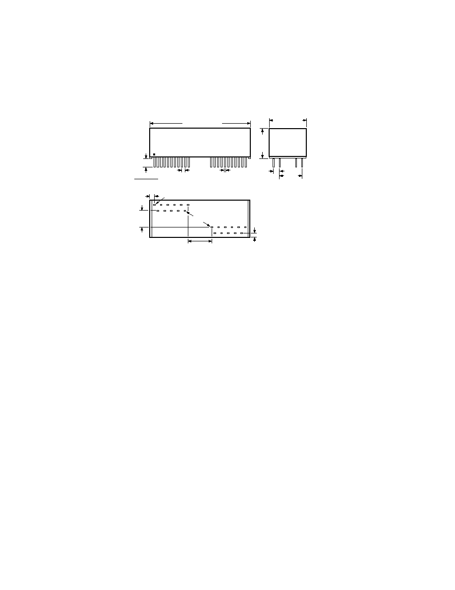
22-Lead Plastic DIP
(ND-22)
BOTTOM
VIEW
SYSTEM
FIELD
0.250
(6.35)
0.050
(1.27)
PIN 1
0.075 (1.91)
* CREEPAGE PATH (SUBTRACT APPROXIMATELY
0.079 (2mm) FOR SOLDER PAD RADII ON PC BOARD.
THIS SPACING SUPPORTS THE INTRINSICALLY
SAFE RATING OF 750V. WAVE SOLDERING IS
NOT RECOMMENDED.
0.350 (8.89)
0.5* (12.2)
SIDE VIEW
22
1
11
12
1.500 (38.1) MAX
0.050 (1.27)
0.160 (4.06)
0.140 (3.56)
0.020 0.010
(0.508 0.254)
22 PLACES
0.100
(2.54)
0.550 (13.97)
MAX
0.440
(11.18)
MAX
END VIEW
0.350
(8.89)
OUTLINE DIMENSIONS
Dimensions shown in inches and (mm).