Äîêóìåíòàöèÿ è îïèñàíèÿ www.docs.chipfind.ru
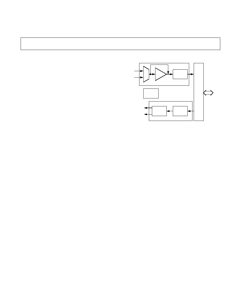
FUNCTIONAL BLOCK DIAGRAM
VOICEBAND
ANALOG
INPUT A
VOICEBAND
ANALOG
INPUT B
DIFFERENTIAL
ANALOG
OUTPUT
DIGITAL
DATA AND
CONTROL
SERIAL
PORT
16-BIT
SIGMA-
DELTA DAC
16-BIT
SIGMA-
DELTA ADC
MUX
+20dB
AMP
VOLTAGE
REFERENCE
PGA
REV. 0
Information furnished by Analog Devices is believed to be accurate and
reliable. However, no responsibility is assumed by Analog Devices for its
use, nor for any infringements of patents or other rights of third parties
which may result from its use. No license is granted by implication or
otherwise under any patent or patent rights of Analog Devices.
a
Voiceband Signal Port
One Technology Way, P.O. Box 9106, Norwood, MA 02062-9106, U.S.A.
Tel: 617/329-4700
Fax: 617/326-8703
AD28msp02
FEATURES
Complete Analog I/O Port for Voiceband DSP
Applications
Linear-Coded 16-Bit Sigma-Delta ADC
Linear-Coded 16-Bit Sigma-Delta DAC
On-Chip Anti-Aliasing and Anti-lmaging Filters
On-Chip Voltage Reference
8 kHz Sampling Frequency
Twos Complement Coding
65 dB SNR + THD
Programmable Gain on DAC and ADC
Serial Interface To DSP Processors
24-Pin DlP/28-Lead SOIC
Single 5 V Power Supply
GENERAL DESCRIPTION
The AD28msp02 Voiceband Signal Port is a complete analog
front end for high performance voiceband DSP applications.
Compared to traditional
µ
-law and A-law codecs, the
AD28msp02's linear-coded ADC and DAC maintain wide
dynamic range while maintaining superior SNR and THD. A
sampling rate of 8.0 kHz coupled with 65 dB SNR + THD per-
formance make the AD28msp02 attractive in many telecom and
speech processing applications, for example digital cellular radio
and high quality telephones. The AD28msp02 simplifies overall
system design by requiring only a single +5 V power supply.
The inclusion of on-chip anti-aliasing and anti-imaging filters,
16-bit sigma-delta ADC and DAC, and programmable gain
amplifiers ensures a highly integrated and compact solution to
voiceband analog processing requirements. Sigma-delta conver-
sion technology eliminates the need for complex off-chip anti-
aliasing filters and sample-and-hold circuitry.
The AD28msp02's serial I/O port provides an easy interface to
host DSP microprocessors such as the ADSP-2101, ADSP-2105
and ADSP-2111. The AD28msp02 is available in a 24-pin, 0.3"
plastic DIP and a 28-lead SOIC package.
FUNCTIONAL DESCRIPTION
Figure 1 shows a block diagram of the AD28msp02.
A/D CONVERSION
The A/D conversion circuitry of the AD28msp02 consists of two
analog input amplifiers, an optional 20 dB preamplifier, and
a sigma-delta analog-to-digital converter (ADC). The analog
input signal to the AD28msp02 must be ac-coupled.
Analog Input Amplifiers
The two analog input amplifiers (NORM, AUX) are internally
biased by an on-chip voltage reference in order to allow opera-
tion of the AD28msp02 with a single +5 V power supply.
An analog multiplexer selects either the NORM or AUX ampli-
fier as the input to the ADC's sigma-delta modulator. The
optional 20 dB preamplifier may be used to increase the signal
level; the preamplifier can be inserted before the modulator or
can be bypassed. Input signal level to the sigma-delta modulator
should not exceed V
INMAX
, which is specified under "Analog
Interface Electrical Characteristics." Refer to "Analog Input" in
the "Design Considerations" section of this data sheet for more
information.
The input multiplexer and 20 dB preamplifier are configured by
Bits 0 and 1 (IPS, IMS) of the AD28msp02's control register. If
the multiplexer setting is changed while an input signal is being
processed, the ADC's output must be allowed time to settle to
ensure that the output data is valid.
ADC
The ADC consists of a 2nd-order analog sigma-delta modulator,
an anti-aliasing decimation filter, and a digital high-pass filter.
The sigma-delta modulator noise-shapes the signal and pro-
duces 1-bit samples at a 1.0 MHz rate. This bit stream, which
represents the analog input signal, is fed to the anti-aliasing
decimation filter.
Decimation Filter
The anti-aliasing decimation filter contains two stages. The first
stage is a sinc
4
digital filter that increases resolution to 16 bits
and reduces the sample rate to 40 kHz. The second stage is an
IIR low-pass filter.
AD28msp02
REV. 0
2
OUTPUT
DIFFERENTIAL
AMP
CONTROL
REGISTER
VOLTAGE
REFERENCE
1
16
16
INPUT
AMP
ANALOG
SIGMA-DELTA
MODULATOR
1.0
MHz
ANTI-ALIASING
DECIMATION
FILTER
DIGITAL
HIGH-PASS
FILTER
8.0
kHz
8.0
kHz
16-BIT SIGMA-DELTA ADC
VFB
NORM
VIN
NORM
16
8.0
kHz
SDI
SDIFS
SDO
SDOFS
SCLK
DATA/
CNTRL
MUX
INPUT
AMP
VFB
AUX
VIN
AUX
+20dB
AMP
NORM
AUX
V
REF
VOUT
P
VOUT
N
CS
1
16
16
1.0
MHz
1.0
MHz
8.0
kHz
16-BIT SIGMA-DELTA DAC
ANTI-IMAGING
INTERPOLATION
FILTER
PGA
SERIAL
PORT
HIGH-PASS
DIGITAL
FILTER
ANALOG
SMOOTHING
FILTER
DIGITAL
SIGMA-DELTA
MODULATOR
Figure 1. AD28msp02 Block Diagram
The IIR low-pass filter is a 10th-order elliptic filter with a pass-
band edge at 3.7 kHz and a stopband attenuation of 65 dB at
4 kHz. This filter has the following specifications:
Filter type:
10th-order low-pass elliptic IIR
Sample frequency:
40.0 kHz
Passband cutoff:*
3.70 kHz
Passband ripple:
±
0.2 dB
Stopband cutoff:
4.0 kHz
Stopband ripple:
65.00 dB
*The passband cutoff frequency is defined to be the last point in the passband
that meets the passband ripple specification.
(Note that these specifications apply only to this filter, and not to the entire
ADC. The specifications can be used to perform further analysis of the exact
characteristics of the filter, for example using a digital filter design software
package.)
Figure 2 shows the frequency response of the IIR low-pass filter.
0
100
5000
80
2000
40
60
20
4400
3800
3200
2600
FREQUENCY Hz
LOG MAGNITUDE dB
Figure 2. IIR Low-Pass Filter Frequency Response
High-Pass Filter
The digital high-pass filter removes frequency components at
the low end of the spectrum; it attenuates signal energy below
the passband of the converter. The high-pass filter can be
bypassed by setting the ADBY bit (Bit 3) of the AD28msp02's
control register.
The high-pass filter is a 4th-order elliptic filter with a passband
cutoff at 150 Hz. Stopband attenuation is 25 dB. This filter has
the following specifications:
Filter type:
4th-order high-pass elliptic IIR
Sample frequency:
8.0 kHz
Passband cutoff:
150.0 Hz
Passband ripple:
±
0.2 dB
Stopband cutoff:
100.0 Hz
Stopband ripple:
25.00 dB
(Note that these specifications apply only to this filter, and not to the entire
ADC. The specifications can be used to perform further analysis of the exact
characteristics of the filter, for example using a digital filter design software
package.)
Figure 3 shows the frequency response of the high-pass filter.
0
100
300
80
0
40
60
20
240
180
120
60
FREQUENCY Hz
LOG MAGNITUDE dB
Figure 3. High-Pass Filter Frequency Response
Passband ripple is
±
0.2 dB for the combined effects of the
ADC's digital filters (i.e., high-pass filter and IIR low-pass of
the decimation filter) in the 300 Hz3400 Hz passband.
The output of the ADC is transferred to the AD28msp02's
serial port (SPORT) at an 8 kHz rate, for transmission to the
host DSP processor. Maximum group delay in the ADC will not
exceed 1 ms in the region from 300 Hz to 3 kHz.

AD28msp02
REV. 0
3
D/A CONVERSION
The D/A conversion circuitry of the AD28msp02 consists of a
sigma-delta digital-to-analog converter (DAC), an analog
smoothing filter, a programmable gain amplifier, and a differen-
tial output amplifier.
DAC
The AD28msp02's sigma-delta DAC implements digital filters
and a sigma-delta modulator with the same characteristics as the
filters and modulator of the ADC. The DAC consists of a digital
high-pass filter, an anti-imaging interpolation filter, and a digital
sigma-delta modulator.
The DAC receives 16-bit samples from the host DSP processor
via AD28msp02's serial port at an 8 kHz rate. If the host pro-
cessor fails to write a new value to the serial port, the existing
(previous) data is read again. The data stream is filtered first by
the DAC's high-pass filter and then by the anti-imaging interpo-
lation filter. These filters have the same characteristics as the
ADC's anti-aliasing decimation filter and digital high-pass filter.
The output of the interpolation filter is fed to the DAC's digital
sigma-delta modulator, which converts the 16-bit data to 1-bit
samples at a 1.0 MHz rate. The modulator noise-shapes the sig-
nal such that errors inherent to the process are minimized in the
passband of the converter. The bit stream output of the sigma-
delta modulator is fed to the AD28msp02's analog smoothing
filter where it is converted to an analog voltage.
High-Pass Filter
The digital high-pass filter of the AD28msp02's DAC has the
same characteristics as the high-pass filter of the ADC. The
high-pass filter removes frequency components at the low end of
the spectrum; it attenuates signal energy below the passband of
the converter. The DAC's high-pass filter can be bypassed by
setting the DABY bit (Bit 2) of the AD28msp02's control
register.
The high-pass filter is a 4th-order elliptic filter with a passband
cutoff at 150 Hz. Stopband attenuation is 25 dB. This filter has
the following specifications:
Filter type:
4th-order high-pass elliptic IIR
Sample frequency:
8.0 kHz
Passband cutoff:
150.0 Hz
Passband ripple:
±
0.2 dB
Stopband cutoff:
100.0 Hz
Stopband ripple:
25.00 dB
(Note that these specifications apply only to this filter, and not to the entire DAC.
The specifications can be used to perform further analysis of the exact characteris-
tics of the filter, for example using a digital filter design software package.)
Figure 3 shows the frequency response of the high-pass filter.
Interpolation Filter
The anti-imaging interpolation filter contains two stages. The
first stage is an IIR low-pass filter that interpolates the data rate
from 8 kHz to 40 kHz and removes images produced by the in-
terpolation process. The output of this stage is then interpolated
to 1.0 MHz and fed to the second stage, a sinc
4
digital filter that
attenuates images produced by the 40 kHz to 1.0 MHz inter-
polation process.
PIN DESCRIPTIONS
Pin Name
I/O/Z Function
VIN
NORM
I
Analog input to inverting terminal of
NORM input amplifier.
VFB
NORM
O
Output terminal of NORM amplifier.
VIN
AUX
I
Analog input to inverting terminal of
AUX input amplifier.
VFB
AUX
O
Output terminal of AUX amplifier.
VOUT
P
O
Analog output from noninverting
terminal of differential output amplifier.
VOUT
N
O
Analog output from inverting terminal of
differential output amplifier.
V
REF
O
On-chip bandgap voltage reference
(2.5 V
±
10%).
MCLK
I
Master clock input; frequency must
equal 13.0 MHz to guarantee listed
specifications.
SCLK
O/Z
Serial clock used to clock data or control
bits to and from the serial port
(SPORT). The frequency of SCLK is
equal to the frequency of the master
clock (MCLK) divided by 5. SCLK is
3-stated when CS is low.
SDI
I
Serial data input of SPORT. Both data
and control information are input on
this pin. Input at SDI is ignored when
CS is low.
SDO
O/Z Serial data output of SPORT. Both data
and control information are output on
this pin. SDO is 3-stated when CS is
low.
SDIFS
I
Framing signal for SDI serial transfers.
Input at SDIFS is ignored when CS is
low.
SDOFS
O/Z
Framing signal for SDO serial transfers.
SDOFS is 3-stated when CS is low.
DATA/CNTRL
I
Configures AD28msp02 for either data
or control information transfers (via
SPORT).
CS
I
Active-high chip select. Can be used to
3-state the SPORT interface; when CS
is low, the SCLK, SDO, and SDOFS
outputs are 3-stated and the SDI and
SDIFS inputs are ignored. If CS is de-
asserted during a serial data transfer, the
16-bit word being transmitted is lost.
RESET
I
Active low reset signal; resets Control
Register and clears digital filters. RESET
does not 3-state the SPORT outputs
(SCLK, SDO, SDOFS).
V
CC
Analog supply voltage; nominal +5 V.
GND
A
Analog ground.
V
DD
Digital supply voltage; nominal +5 V.
GND
D
Digital ground.
AD28msp02
REV. 0
4
The IIR low-pass filter is a 10th-order elliptic filter with a pass-
band edge at 3.70 kHz and a stopband attenuation of 65 dB at
4 kHz. This filter has the following specifications:
Filter type:
l0th-order low-pass elliptic IIR
Sample frequency:
40.0 kHz
Passband cutoff:*
3.70 kHz
Passband ripple:
±
0.2 dB
Stopband cutoff:
4.0 kHz
Stopband ripple:
65.00 dB
*The passband cutoff frequency is defined to be the last point in the passband
that meets the passband ripple specification.
(Note that these specifications apply only to this filter, and not to the entire
DAC. The specifications can be used to perform further analysis of the exact
characteristics of the filter, for example using a digital filter design software
package.)
Figure 2 shows the frequency response of the IIR low-pass filter.
Passband ripple is
±
0.2 dB for the combined effects of the
DAC's digital filters (i.e., high-pass filter and IIR low pass of the
interpolation filter) in the 300 Hz3400 Hz passband.
Analog Smoothing Filter and Programmable Gain Amplifier
The programmable gain amplifier (PGA) can be used to adjust
the output signal level by 15 dB to +6 dB. This gain is selected
by bits 79 (OG0, OG1, OG2) of the AD28msp02's control
register.
The AD28msp02's analog smoothing filter consists of a 2nd-
order Sallen-Key continuous-time filter and a 3rd-order
switched capacitor filter. The Sallen-Key filter has a 3 dB point
at approximately 80 kHz.
Differential Output Amplifier
The AD28msp02's analog output (VOUT
P
, VOUT
N
) is pro-
duced by a differential output amplifier. The differential ampli-
fier can drive loads of 2 k
or greater and has a maximum
differential output voltage swing of
±
3.156 V peak-to-peak
(3.17 dBm0). The output signal is dc-biased to the
AD28msp02's on-chip voltage reference (V
REF
) and can be
ac-coupled directly to a load or dc-coupled to an external ampli-
fier. Refer to "Analog Output" in the "Design Considerations"
section of this data sheet for more information.
The VOUT
P
VOUT
N
outputs must be used as differential out-
puts; do not use either as a single-ended output.
SERIAL PORT
The AD28msp02 communicates with a host processor via the
bidirectional synchronous serial port (SPORT). The SPORT is
used to transmit and receive digital data and control information.
All serial transfers are 16 bits long, MSB first. Data bits are
transferred at the serial clock rate (SCLK). SCLK equals the
master clock frequency divided by 5. SCLK = 2.6 MHz for the
master clock frequency MCLK = 13.0 MHz.
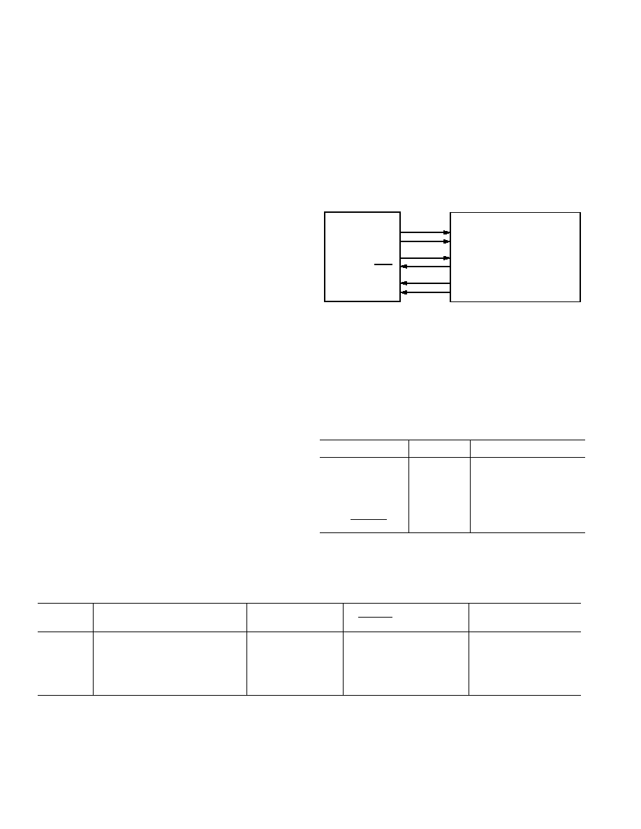
Host Processor Interface
The AD28msp02-to-host processor interface is shown in Figure 4.
AD28msp02
SDO
SERIAL DATA RECEIVE
SDOFS
RECEIVE FRAME SYNC
SCLK
SERIAL CLOCK
SDI
SERIAL DATA TRANSMIT
SDIFS
TRANSMIT FRAME SYNC
Host Processor
DATA/CNTRL
FLAG
Figure 4. AD28msp02-to-Host Processor Interface
Table I describes the SPORT signals and how they are used to
communicate with the host processor. The AD28msp02's chip
select (CS) must be held high to enable SPORT operation. CS
can be used to 3-state the SPORT pins and disable communica-
tion with the host processor.
To use the ADSP-2101 or ADSP-2111 as host DSP processor
for the AD28msp02, the following connections can be used (as
shown in Figure 5):
AD28msp02 Pin
ADSP-2101/2111 Pin
SCLK
SCLK0
SDO
DR0
SDOFS
RFS0
SDI
DT0
SDIFS
TFS0
DATA/CNTRL
FO (Flag Output)
Table I. SPORT Signals
Signal
Signal State When
Signal State During
Name
Description
Generated By
RESET
Low (CS High)
Powerdown (CS High)
SCLK
Serial clock
AD28msp02
Low
Active
SDO
Serial data output
AD28msp02
Low
Active*
SDOFS
Serial data output frame sync
AD28msp02
Low
Low
SDI
Serial data input
Host Processor
--
--
SDIFS
Serial data input frame sync
Host Processor
--
--
(CS must be held high to enable SPORT operation.)
*Outputs last data value that was valid prior to entering powerdown.
AD28msp02
REV. 0
5
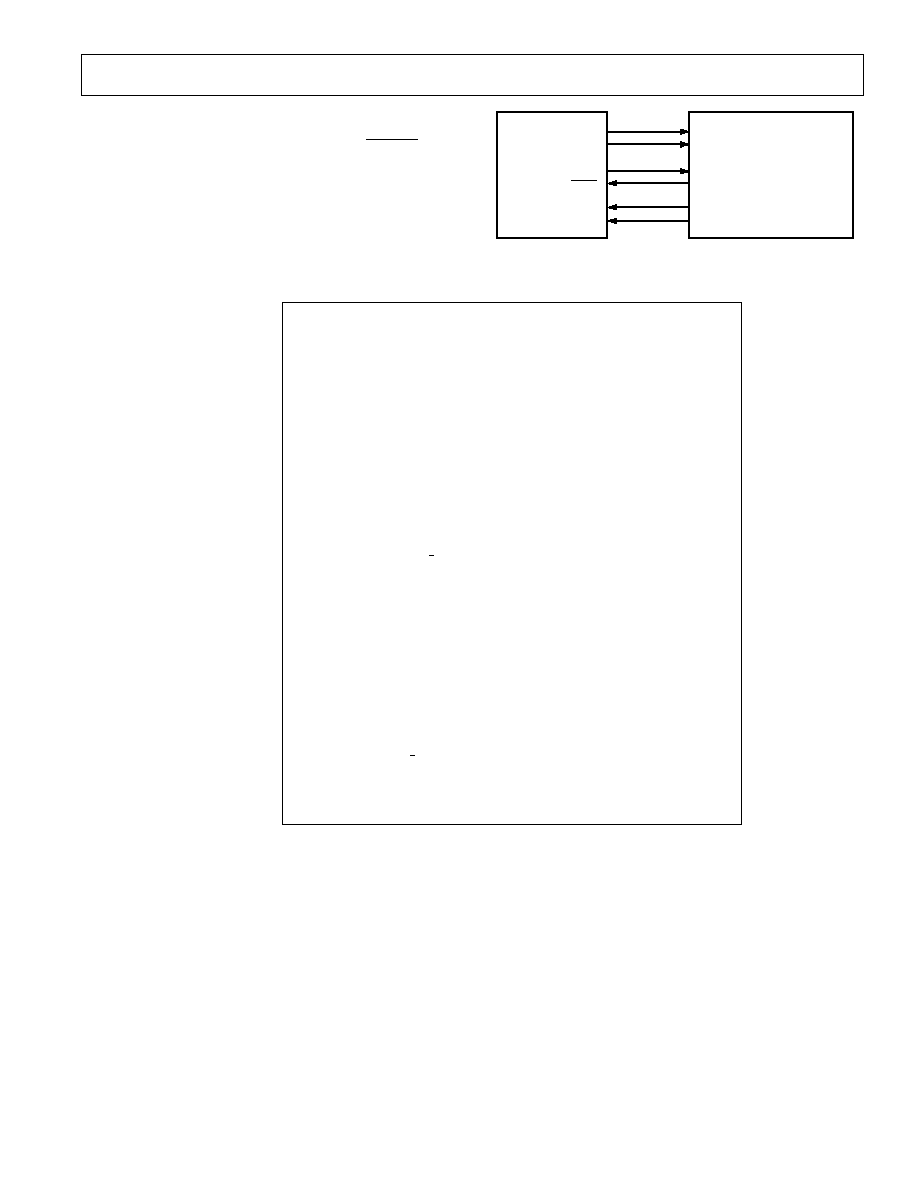
Note that the ADSP-2101's SPORT0 communicates with the
AD28msp02's SPORT while the ADSP-2101's Flag Output
(FO) is used to signal the AD28msp02's DATA/CNTRL input.
SPORT1 on the ADSP-2101 must be configured for flags and
interrupts in this system.
Figure 6 shows an ADSP-2101 assembly language program that
initializes the AD28msp02 and implements digital loopback
through the DSP processor.
SDO
SDOFS
SCLK
DATA/CNTRL
SDI
SDIFS
AD28msp02
DR0
RFS0
SCLK0
FO
DT0
TFS0
ADSP-2101
Figure 5. AD28msp02-to-ADSP-2101 Interface
{ This ADSP-2101 program initializes the AD28msp02 }
{ and executes a loopback, or talk-through, routine. }
.MODULE/ABS = 0/BOOT = 0 test1;
resetv:
JUMP begin;
{restart}
RTI; RTI; RTI;
irq2v:
RTI; RTI; RTI; RTI;
{IRQ2}
st0x:
RTI; RTI; RTI; RTI;
{SPORT0 Tx}
sr0x:
ax0 = rx0;
{SPORT0 Rx}
tx0 = ax0;
RTI; RTI;
irq1v:
RTI; RTI; RTI; RTI;
{irq1}
irq0v:
RTI; RTI; RTI; RTI;
{irq0}
timerv:
RTI; RTI; RTI; RTI;
begin:
RESET FLAG OUT;
AX0 = 0x2A0F;
{Configure ADSP-2101 SPORT0 for }
DM (0x3FF6) = AX0;
{ ext. SCLK, ext. RFS, int. TFS }
AX0 = 0x101F;
{ Enable ADSP-2101 SPORT0, }
DM (0x3FFF) = AX0;
{ configure SPORT1 for Flag Out }
IMASK= 0x10;
AX0 = 0x30;
{ Write control word to take}
TX0 = AX0;
{ AD28msp02 out of powerdown }
IDLE;
NOP;
IMASK= 0x08;
SET FLAG OUT;
wait:
JUMP wait;
{ Wait for receive interrupt }
NOP;
.ENDMOD;
Figure 6. ADSP-2101 Digital Loopback Routine
Document Outline
- Specifications
- Pinout
- Package drawings
- Ordering Guide
- Features
- Product Description
- Absolute Maximum Ratings
- Functional Block Diagram
- FUNCTIONAL DESCRIPTION
- A/D CONVERSION
- ADC
- PIN DESCRIPTIONS
- D/A CONVERSION
- DAC
- SERIAL PORT
- CONTROL REGISTER
- DESIGN CONSIDERATIONS
- DEFINITION OF SPECIFICATIONS
- RECOMMENDED OPERATING CONDITIONS
- ESD SENSITIVITY
- DIGITAL INTERFACE ELECTRICAL CHARACTERISTICS
- ANALOG INTERFACE ELECTRICAL CHARACTERISTICS
- POWER DISSIPATION
- TIMING PARAMETERS
- DIGITAL TEST CONDITIONS
- GAIN
- FREQUENCY RESPONSE
- NOISE AND DISTORTION
- ORDERING GUIDE
- DIAGRAMS
- Block Diagram
- AD28msp02-to-Host Processor Interface
- AD28msp02-to-ADSP-2101 Interface
- Recommended Analog Input Circuit
- Example Analog Input Circuit for 0 dB Gain
- Example Circuit for Differential Output
- Example Circuit for Single-Ended Output
- Serial Output Startup Time
- Clock Signals
- Serial Port 3-State
- Serial Ports
- Voltage Reference Levels for AC Measurements
- Equivalent Device Loading for AC Measurements