 | ÐлекÑÑоннÑй компоненÑ: AD2S100AP | СкаÑаÑÑ:  PDF PDF  ZIP ZIP |
Äîêóìåíòàöèÿ è îïèñàíèÿ www.docs.chipfind.ru
One Technology Way, P.O. Box 9106, Norwood, MA 02062-9106, U.S.A.
Tel: 617/329-4700
Fax: 617/326-8703
REV. A
Information furnished by Analog Devices is believed to be accurate and
reliable. However, no responsibility is assumed by Analog Devices for its
use, nor for any infringements of patents or other rights of third parties
which may result from its use. No license is granted by implication or
otherwise under any patent or patent rights of Analog Devices.
a
AD2S100
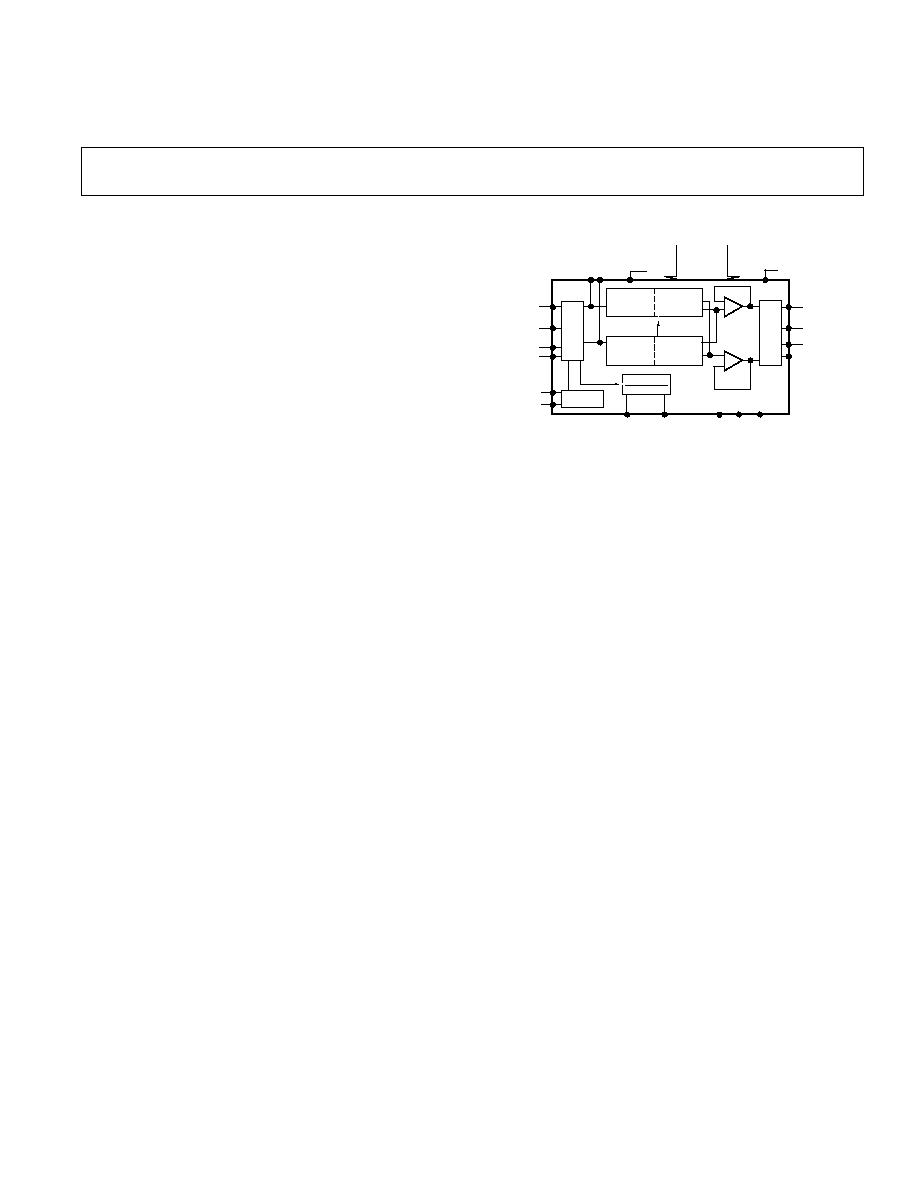
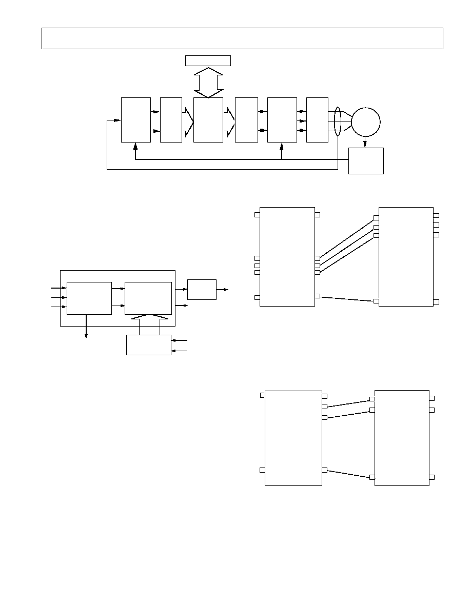
FUNCTIONAL BLOCK DIAGRAM
GENERAL DESCRIPTION
The AD2S100 performs the vector rotation of three-phase 120
degree or two-phase 90 degree sine and cosine signals by trans-
ferring these inputs into a new reference frame which is controlled
by the digital input angle
. Two transforms are included in the
AD2S100. The first is the Clarke transform which computes
the sine and cosine orthogonal components of a three-phase
input. These signals represent real and imaginary components
which then form the input to the Park transform. The Park
transform relates the angle of the input signals to a reference
frame controlled by the digital input port. The digital input
port is a 12-bit parallel binary representation.
If the input signals are represented by Vds and Vqs, respectively,
where Vds and Vqs are the real and imaginary components, then
the transformation can be described as follows:
Vds' = Vds Cos
Vqs Sin
Vqs' = Vds Sin
+ Vqs Cos
Where Vds' and Vqs' are the output of the Park transform
and Sin
, and Cos
are the values internally derived by the
AD2S100 from the binary digital data.
The input section of the device can be configured to accept
either three-phase inputs, two-phase inputs of a three-phase
system, or two 90 degree input signals. The homopolar output
detects the imbalance of a three-phase input only. Under nor-
mal conditions, this output will be zero.
The digital input section will accept a resolution of up to 12 bits
(AD2S100). An input data strobe signal is required to synchro-
nize the position data and load this information into the device
counters. A busy output is provided to identify the conversion
status of the AD2S100. The busy period represents the conver-
sion time of the vector rotation.
Two analog output formats are available. A two-phase rotated
output facilitates multiple rotation blocks. Three phase format
signals are available for use with a PWM inverter.
PRODUCT HIGHLIGHTS
Hardware Peripheral for Standard Microcontrollers and
DSP Systems
The AD2S100 removes the time consuming cartesian transfor-
mations from digital processors and benchmarks a speed im-
provement of 30:1 on standard 20 MHz processors. AD2S100
transformation time = 2
µ
s (typ).
Field Oriented Control of AC and DC Brushless Motors
The AD2S100 accommodates all the necessary functions to
provide a hardware solution for ac vector control of induction
motors and dc brushless motors.
Three-Phase Imbalance Detection
The AD2S100 can be used to sense overcurrent situations or
imbalances in a three-phase system via the homopolar output.
Resolver-to-Digital Converter Interface
The AD2S100 provides general purpose interface for position
sensors used in the application of dc brushless and ac induction
motor control.
Ia
Ib
Ic
Vds
Vqs
SECTOR
MULTIPLIER
SINE AND
COSINE
MULTIPLIER
INPUT
DATA
STROBE
HOMOPOLAR
OUTPUT
HOMOPOLAR
REFERENCE
+5V GND 5V
POSITION
PARALLEL
DATA
12 BITS
Cos (
+
120
° +
)
Cos (
+
240
° +
)
Va
Vb
Vc
30-20
Sin
Cos
Cos
Sin
Cos
+
CONV1
CONV2
DECODE
BUSY
Vds'
Vqs'
Sin
+
SECTOR
MULTIPLIER
SINE AND
COSINE
MULTIPLIER
Ia + Ib + Ic
3
2
-3
Cos (
+
120
°)
Cos (
+
240
°)
AC Vector Processor
FEATURES
Complete Vector Coordinate Transformation on Silicon
Mixed Signal Data Acquisition
Three-Phase 120 and Orthogonal 90 Signal
Transformation
Three-Phase Balance DiagnosticHomopolar Output
APPLICATIONS
AC Induction and DC Permanent
Magnet Motor Control
HVAC, Pump, Fan Control
Material Handling
Robotics
Spindle Drives
Gyroscopes
Dryers
Washing Machines
Electric Cars
Actuator
Three-Phase Power Measurement
Digital-to-Resolver & Synchro Conversion

AD2S100SPECIFICATIONS
Parameter
Min
Typ
Max
Units
Conditions
SIGNAL INPUTS
PH/IP1, 2, 3, 4 Voltage Level
±
2.8
3.3
V p-p
DC to 50 kHz
PH/IPH1, 2, 3 Voltage Level
±
4.25
V p-p
DC to 50 kHz
Input Impedance
PH/IP1, 2, 3
7.5
10
k
PH/IPH1, 2, 3
13.5
18
k
PH/IP1, 4
1
M
Mode 1 Only (2 Phase) Sin & Cos
Gain
PH/IP1, 2, 3, 4
0.98
1
1.02
PH/IPH1, 2, 3
0.56
VECTOR PERFORMANCE
3
Input-Output
Radius Error (Any Phase)
0.35
0.7
%
DC to 600 Hz
Angular Error
1, 2
(PH/IP)
9
18
arc min
DC to 600 Hz
(PH/IPH)
24
arc min
DC to 600 Hz
Monotonicity
Guaranteed Monotonic
Full Power Bandwidth
50
kHz
Small Signal Bandwidth
200
kHz
ANALOG SIGNAL OUTPUTS
PH/OP1, 2, 3, 4
PH/IP, PH/IPH INPUTS
Output Voltage
3
±
2.8
±
3.3
V p-p
DC to 50 kHz
Offset Voltage
2
5
mV
Inputs = 0 V
Slew Rate
2
V/
µ
s
Small Signal Step Response
1
µ
s
1
°
Input to Settle to
±
1 LSB
(Input to Output)
Output Resistance
15
Output Drive Current
3.0
4.0
mA
Outputs to AGND
Resistive Load
2
k
Capacitive Load
50
pF
STROBE
Write
100
ns
Positive Pulse
Max Update Rate
366
kHz
BUSY
Pulse Width
1.7
2.5
µ
s
Conversion in Process
V
OH
4
V dc
I
OH
= 0.5 mA
V
OL
1
V dc
I
OL
= 0.5 mA
DIGITAL INPUTS
DB1DB12
V
IH
3.5
V dc
V
IL
1.5
V dc
Input Current, I
IN
10
µ
A
Input Capacitance, C
IN
10
pF
CONVERT MODE
(CONV1, CONV2)
V
IH
3.5
V dc
Internal 50 k
Pull-Up Resistor
V
IL
1.5
V dc
Input Current
100
µ
A
Input Capacitance
10
pF
CONVERT LOGIC
CONV1 CONV2
NO CONNECT
DGND
2-Phase Orthogonal with 2 Inputs
Nominal Input Level
DGND
V
DD
3-Phase (0
°
, 120
°
, 240
°
) with 3 Inputs
Nominal Input Level
V
DD
V
D D
3-Phase (0
°
, 120
°
, 240
°
) with 2 Inputs
Nominal Input Level
REV. A
2
(V
DD
= +5 V 5%; V
SS
= 5 V 5% AGND = DGND = O V; T
A
= 40 C to
+85
°
C, unless otherwise noted)

Parameter
Min
Typ
Max
Units
Conditions
HOMOPOLAR OUTPUT
HPOPOutput
V
OH
4
V dc
I
OH
= 0.5 mA
V
OL
1
V dc
I
OL
= 0.5 mA
HPREFREFERENCE
0.5
V dc
Homopolar Output-Internal
I
SOURCE
= 25
µ
A and 20 k
to AGND
HPFILT-FILTER
100
k
Internal Resistor with External
Capacitor = 220 nF
POWER SUPPLY
V
DD
4.75
5
5.25
V dc
V
SS
5.25
5
4.75
V dc
I
DD
4
10
mA
Quiescent Current
I
SS
4
10
mA
Quiescent Current
NOTES
1
Angular accuracy includes offset and gain errors. Stationary digital input and maximum analog frequency inputs.
2
Included in the angular error is an allowance for the additional error caused by the phase delay as a function of input frequency. For example, if
f
INPUT
= 600 Hz, the contribution to the error due to phase delay is: 650 ns
×
f
INPUT
×
60
×
360 = 8.4 arc minutes.
3
Output subject to input voltage and gain.
Specifications in boldface are production tested.
Specifications subject to change without notice.
AD2S100
REV. A
3
RECOMMENDED OPERATING CONDITIONS
Power Supply Voltage (+V
DD
, V
SS
) . . . . . . . . .
±
5 V dc
±
5%
Analog Input Voltage (PH/IP1, 2, 3, 4) . . . . . . 2 V rms
±
10%
Analog Input Voltage (PH/IPH1, 2, 3) . . . . . . 3 V rms
±
10%
Ambient Operating Temperature Range
Industrial (AP) . . . . . . . . . . . . . . . . . . . . . . . 40
°
C to +85
°
C
ORDERING GUIDE
Model
Temperature Range
Accuracy
Option*
AD2S100AP
40
°
C to +85
°
C
18 arc min
P-44A
*P = Plastic Leaded Chip Carrier.
ABSOLUTE MAXIMUM RATINGS
(T
A
= +25
°
C)
V
DD
to AGND . . . . . . . . . . . . . . . . . . . . . . . 0.3 V to +7 V dc
V
SS
to AGND . . . . . . . . . . . . . . . . . . . . . . . +0.3 V to 7 V dc
AGND to DGND . . . . . . . . . . . . . . . . . . . . . . . . . . .
±
0.3 V dc
Analog Input Voltage to AGND . . . . . . . . . . . . . . . V
SS
to V
DD
Digital Input Voltage to DGND . . . . 0.3 V to V
DD
+ 0.3 V dc
Digital Output Voltage to DGND . . . 0.3 V to V
DD
+ 0.3 V dc
Analog Output Voltage to AGND
. . . . . . . . . . . . . . . . . . . . . . V
SS
0.3 V to V
DD
+ 0.3 V dc
Analog Output Load Condition (PH/OP1, 2, 3, 4
Sin
, Cos
) . . . . . . . . . . . . . . . . . . . . . . . . . . . . . . . . . . . . . . . 2
k
Power Dissipation . . . . . . . . . . . . . . . . . . . . . . . . . . . . . 60 mW
Operating Temperature
Industrial (AP) . . . . . . . . . . . . . . . . . . . . . . . 40
°
C to +85
°
C
Storage Temperature . . . . . . . . . . . . . . . . . 65
°
C to +150
°
C
Lead Temperature (Soldering, 10 sec) . . . . . . . . . . . . . +300
°
C
CAUTION
1. Absolute Maximum Ratings are those values beyond which
damage to the device may occur.
2. Correct polarity voltages must be maintained on the +V
DD
and V
SS
pins.
WARNING!
ESD SENSITIVE DEVICE
CAUTION
ESD (electrostatic discharge) sensitive device. Electrostatic charges as high as 4000 V readily
accumulate on the human body and test equipment and can discharge without detection.
Although the AD2S100 features proprietary ESD protection circuitry, permanent damage may
occur on devices subjected to high energy electrostatic discharges. Therefore, proper ESD
precautions are recommended to avoid performance degradation or loss of functionality.
AD2S100
REV. A
4
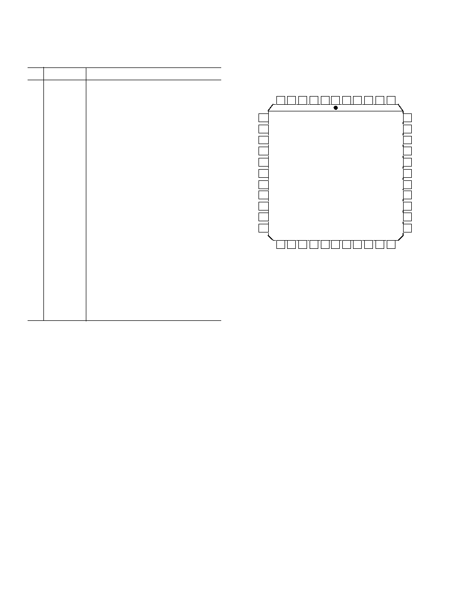
PIN DESIGNATIONS
1, 2, 3
Pin
Mnemonic Description
3
STROBE
Begin Conversion
4
V
DD
Positive Power Supply
5
V
SS
Negative Power Supply
6
PH/OP4
Sin (
+ )
7
PH/OP1
Cos (
+ )
8
PH/OP3
Cos (
+
240
°
+
)
9
PH/OP2
Cos (
+ 120
°
+
)
10
AGND
Analog Ground
11
PH/IP4
Sin
Input
12
PH/IPH3
High Level Cos (
+ 240
°
) Input
13
PH/IP3
Cos (
+ 240
°
) Input
14
PH/IPH2
High Level Cos (
+ 120
°
) Input
15
PH/IP2
Cos (
+ 120
°
) Input
16
PH/IPH1
High Level Cos
Input
17
PH/IP1
Cos
()
Input
19
V
SS
Negative Power Supply
20
HPREF
Homopolar Reference
21
HPOP
Homopolar Output
22
HPFILT
Homopolar Filter
23
CONV1
Select Input Format (3 Phase/3 Wire, Sin
24
CONV2
Cos
/Input, 3 Phase/2 Wire)
25
COS
Cos Output
26
SIN
Sin Output
27
DB12
(DB1 = MSB, DB12 = LSB
38
DB1
Parallel Input Data)
41
V
DD
Positive Power Supply
42
DGND
Digital Ground
44
BUSY
Conversion in Progress
NOTES
Signal Inputs Ph/IP and PH/IPH on Pin Nos 11 through 17.
1
90
°
orthogonal signals = Sin
, Cos
(Resolver) = PH/IP4 and PH/IP1.
2
Three phase, 120
°
, three-wire signals
= Cos
, Cos (
+ 120
°
), Cos (
+ 240
°
).
= PH/IP1, PH/IP2, PH/IP3
High Level = PH/IPH1, PH/IPH2, PH/IPH3.
3
Three Phase, 120
°
, two-wire signals = Cos (
+ 120
°
), Cos (
+ 240
°
)
= PH/IP2, PH/IP3.
In all cases where any of the input Pins 11 through 17 are not used, they must
be left unconnected.
PIN CONFIGURATION
6
5
4
3
2
1
44
43
42
41
40
18
19
20
21
22
23
24
25
26
27
28
29
30
31
32
33
34
35
36
37
38
39
V
SS
V
DD
STROBE
NC
NC
BUSY
DGND
V
DD
NC
NC
V
SS
HPREF
HPOP
CONV1
CONV2
COS
DB12
HPFILT
DB11
NC = NO CONNECT
TOP VIEW
(NOT TO SCALE)
AD2S100
PH/OP4
NC
SIN
7
8
11
12
13
14
15
16
17
9
10
NC
DB1
DB2
DB3
DB4
DB5
DB6
DB7
DB8
DB9
DB10
PH/OP1
PH/OP3
PH/OP2
AGND
PH/IP4
PH/IPH3
PH/IP3
PH/IPH2
PH/IP2
PH/IPH1
PH/IP1
AD2S100
REV. A
5
To relate these stator current to the reference frame the rotor
currents assume the same rectangular coordinates, but are now
rotated by the operator e
j
, where e
j
= Cos + jSin .
Here the term vector rotator comes into play where the stator
current vector can be represented in rotor-based coordinates or
vice versa.
The AD2S100 uses e
j
as the core operator. Here represents
the digital position angle which rotates as the rotor moves. In
terms of the mathematical function, it rotates the orthogonal i
ds
and i
qs
components as follows:
i
ds
' + ji
qs
' = (I
ds
+ jI
qs
) e
j
where i
ds
', i
qs
' = stator currents in the rotor reference frame. And
e
j
= Cos + jSin
= (I
ds
+ jI
qs
)(Cos + jSin )
The output from the AD2S100 takes the form of:
i
ds
' = I
ds
Cos I
qs
Sin
i
qs
' = I
ds
Sin + I
qs
Cos
The matrix equation is:
[
i
ds
'
]
=
[
Cos
Sin
] [
I
ds
]
i
qs
'
Sin
Cos
I
qs
and it is shown in Figure 2.
i
ds
i
qs
i
ds
'
i
qs
'
e
j
Figure 2. AD2S100 Vector Rotation Operation
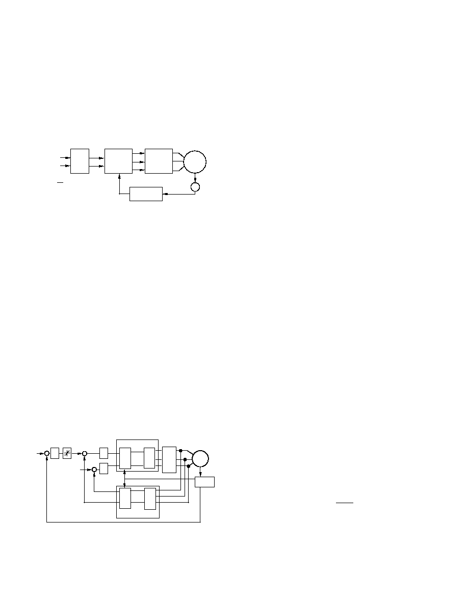
DIGITAL
LATCH
3
+ 2
TRANSFORMATION
SINE AND
COSINE
MULTIPLIER
(DAC)
SINE AND
COSINE
MULTIPLIER
(DAC)
Cos(
+
)
Cos(
+(120
°
+
))
Cos(
+(240
°
+
))
PARK
OUTPUT CLARK
COS
COS
+ 120
°
COS
+ 240
°
SIN
2
3
INPUT CLARK
LATCH
LATCH
Figure 3. Converter Operation Diagram
THEORY OF OPERATION
A fundamental requirement for high quality induction motor
drives is that the magnitude and position of the rotating air-gap
rotor flux be known. This is normally carried out by measuring
the rotor position via a position sensor and establishing a rotor
reference frame that can be related to stator current coordinates.
To generate a flux component in the rotor, stator current is ap-
plied. A build-up of rotor flux is concluded which must be
maintained by controlling the stator current, i
ds
, parallel to the
rotor flux. The rotor flux current component is the magnetizing
current, i
mr
.
Torque is generated by applying a current component which is
perpendicular to the magnetizing current. This current is nor-
mally called the torque generating current, i
qs
.
To orient and control both the torque and flux stator current
vectors, a coordinate transformation is carried out to establish a
new reference frame related to the rotor. This complex calcula-
tion is carried out by the AD2S100 vector processor.
To expand upon the vector operator a description of a single
vector rotation is of assistance. If it is considered that the mod-
uli of a vector is OP and that through the movement of rotor
position by , we require the new position of this vector it can
be deduced as follows:
Let original vector OP = A (Cos + jSIN ) where A is a
constant;
so if
OQ = OP e
j
(1)
and: e
j
= Cos + jSin
OQ = A (Cos ( +
) + jSin ( + ))
= A [Cos Cos
Sin Sin
+ jSin Cos
+ jCos Sin
]
= A [(Cos + jSin ) (Cos
+ jSin )]
(2)
+
Q
P
O
a
d
Figure 1. Vector Rotation in Polar Coordinate
The complex stator current vector can be represented as i
s
= i
as
+ ai
bs
+ a
2
i
cs
where a = e
j 2
3
and a
2
= e
j 4
3
. This can be re-
placed by rectangular coordinates as
i
s
= i
ds
+ ji
qs
(3)
In this equation i
ds
and i
qs
represent the equivalent of a two-
phase stator winding which establishes the same magnitude of
MMF in a three-phase system. These inputs can be seen after
the three-phase to two-phase transformation in the AD2S100
block diagram. Equation (3) therefore represents a three-phase
to two-phase conversion.
AD2S100
REV. A
6
ANALOG SIGNAL INPUT AND OUTPUT CONNECTIONS
Input Analog Signals
All analog signal inputs to AD2S100 are voltages. There are two
different voltage levels of three-phase (0
°
, 120
°
, 240
°
) signal in-
puts. One is the nominal level, which is
±
2.8 V dc or 2 V rms
and the corresponding input pins are PH/IP1 (Pin 17), PH/IP2
(Pin 15), PH/IP3 (Pin 13) and PH/IP4 (Pin 11).
The high level inputs can accommodate voltages from nominal
up to a maximum of
±
V
DD
/V
SS
. The corresponding input pins
are PH/IPH1 (Pin 16), PH/IPH2 (Pin 14) and PH/IPH3 (Pin
12). The homopolar output can only be used in the three-phase
connection mode.
The converter can accept both two-phase format and three-
phase format input signals. For the two-phase format input, the
two inputs must be orthogonal to each other. For the three-
phase format input, there is the choice of using all three inputs
or using two of the three inputs. In the latter case, the third in-
put signal will be generated internally by using the information
of other two inputs. The high level input mode, however, can
only be selected with three-phase/three-input format. All these
different conversion modes, including nominal/high input level
and two/three-phase input format can be selected using two se-
lect pins (Pin 23, Pin 24). The functions are summarized in
Table I.
Table I. Conversion Mode Selection
CONV1
CONV2
Mode
Description
(Pin 23)
(Pin 24)
MODE1
2-Phase Orthogonal with 2 Inputs
NC
DGND
Nominal Input Level
MODE2
3-Phase (0
°
, 120
°
, 240
°
) with 3 Inputs
DGND
V
DD
Nominal/High Input Level*
MODE3
3-Phase (0
°
, 120
°
, 240
°
) with 2 Inputs
V
DD
V
DD
Nominal Input Level
*The high level input mode can only be selected with MODE2.
MODE1: 2-Phase/2 Inputs with Nominal Input Level
In this mode, PH/IP1 and PH/IP4 are the inputs and the Pins
12 through 16 must be left unconnected.
MODE2: 3-Phase/3 Inputs with Nominal/High Input Level
In this mode, either nominal or high level inputs can be used.
For nominal level input operation, PH/IP1, PH/IP2 and PH/IP3
are the inputs, and there should be no connections to PH/IPH1,
PH/IPH2 and PH/IPH3; similarly, for high level input opera-
tion, the PH/IPH1, PH/IPH2 and PH/IPH3 are the inputs, and
there should be no connections to PH/IP1, PH/IP2 and PH/IP3.
In both cases, the PH/IP4 should be left unconnected. For high
level signal input operation, select MODE2 only.
MODE3: 3-Phase/2 Inputs with Nominal Input Level
In this mode, PH/IP2 and PH/IP3 are the inputs and the third
signal will be generated internally by using the information of
other two inputs. It is recommended that PH/IP1, PH/IPH1,
PH/IPH2, PH/IP4 and PH/IPH3 should be left unconnected.
CONVERTER OPERATION
The architecture of the AD2S100 is illustrated in Figure 3. The
AD2S100 is configured in the forward transformation which ro-
tates the stator coordinates to the rotor reference frame.
Forward Rotation
In this configuration the 3
2
Clark is bypassed, and inputs are
fed directly into the quadrature (PH/IP4) and direct (PH/ IPI)
inputs to the Park transform, e
i
, where
is defined by the
AD2S100's digital input. Position data,
, is loaded into the in-
put latch on the positive edge of the strobe pulse. (For detail on
the timing, please refer to the "timing diagram.") The negative
edge of the strobe signifies that conversion has commenced. A
busy pulse is subsequently produced as data is passed from the
input latches to the Sin and Cos multipliers. During the loading
of the multiplier, the busy pulse remains high to ensure simulta-
neous setting of
in both the Sin and Cos registers.
The negative edge of the busy pulse signifies that the multipliers
are set up and the orthogonal analog inputs are multiplied real
time. The resultant two outputs are accessed via the PH/OPI
(Pin 7) and PH/OP4 (Pin 6), alternatively they can be directly
applied to the output Clark transform. The Clark output is the
vector sum of the analog input vector (Cos
(PH/OPl), Cos (
+
120
°
) (PH/OP2), Cos (
+ 240
°
) (PH/OP3) and the digital in-
put vector
.
For other configurations, please refer to "Forward and Reverse
Transformation."
CONNECTING THE CONVERTER
Power Supply Connection
The power supply voltages connected to V
DD
and V
SS
pins
should be +5 V dc and 5 V dc and must not be reversed. Pin 4
(V
DD
) and Pin 41 (V
DD
) should both be connected to +5 V;
similarly, Pin 5 (V
SS
) and Pin 19 (V
SS
) should both be con-
nected to 5 V dc.
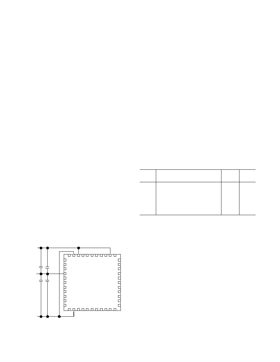
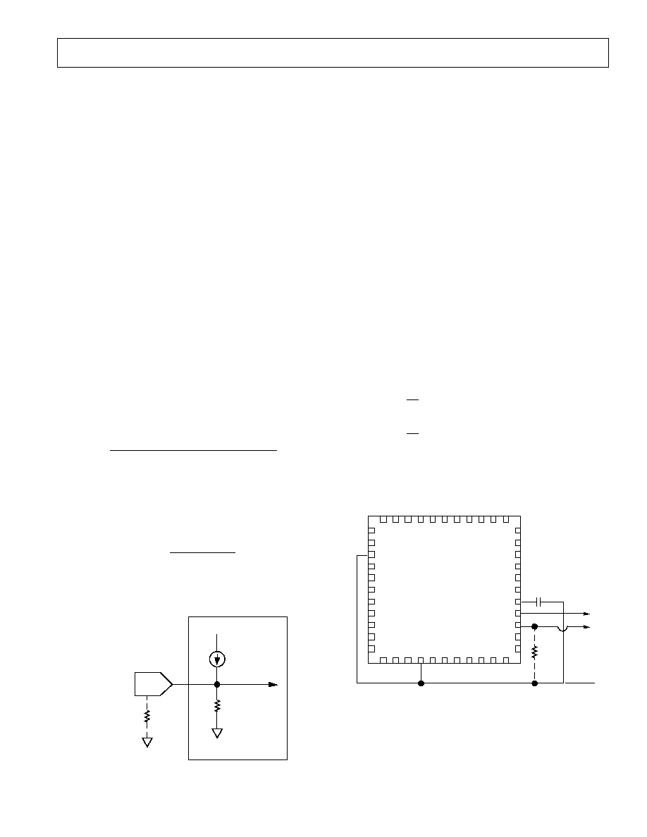
It is recommended that decoupling capacitors, 100 nF (ceramic)
and 10
µ
F (tantalum) or other high quality capacitors, are con-
nected in parallel between the power line V
DD
, V
SS
and AGND
adjacent to the converter. Separate decoupling capacitors should
be used for each converter. The connections are shown in Fig-
ure 4.
AD2S100
TOP VIEW
1
23
12
34
V
DD
V
SS
V
SS
V
DD
AGND
100nF
100nF
10µF
10µF
+
+
+5V
GND
5V
Figure 4. AD2S100 Power Supply Connection
AD2S100
REV. A
7
Output Analog Signals
There are three forms of analog output from the AD2S100.
Sin/Cos orthogonal output signals are derived from the Clark/
three-to-two-phase conversion before the Park angle rotation.
These signals are available on Pin 25 (Cos ) and Pin 26 (Sin
), and occur before Park angle rotation.
Three-Phase Output Signals
(Cos (
+
), Cos (
+
+ 120
°
), Cos (
+
+ 240
°
)), where
represents digital input angle. These signals are available on
Pin 7 (PH/OP1), Pin 9 (PH/OP2) and Pin 8 (PH/OP3),
respectively.
Two-Phase (Sin (
+
), Cos (
+
)) Signals
These represent the output of the coordinate transformation.
These signals are available on Pin 6 (PH/OP4, Sin (
+
)) and
Pin 7 (PH/OP1, Cos (
+
)).
HOMOPOLAR OUTPUT
HOMOPOLAR Reference
In a three-phase ac system, the sum of the three inputs to the
converter can be used to indicate whether or not the phases are
balanced.
If V
SUM
= PH/IP1 + PH/IP2 + PH/IP3 (or PH/IPH1 +
PH/IPH2 + PH/IPH3) this can be rewritten as V
SUM
= [Cos , +
Cos ( + 120
°
) + Cos ( + 240
°
)] = 0. Any imbalances in the
line will cause the sum V
SUM
0. The AD2S100 homopolar
output (HPOP) goes high when V
SUM
> 3
×
V
ts
. The voltage
level at which the HPOP indicates an imbalance is determined
by the HPREF threshold, V
ts
. This is set internally at
±
0.5 V dc
(
±
0.1 V dc). The HPOP goes high when
V
ts
<
(Cos
+
Cos(
+
120
°
)
+
Cos(
+
240
°
))
3
×
V
where V is the nominal input voltage.
With no external components V
SUM
must exceed
±
1.5 V dc in
order for HPOP to indicate an imbalance. The sensitivity of the
threshold can be reduced by connecting an external resistor be-
tween HPOP and ground in Figure 5 where,
V
ts
=
0.5 R
EXT
R
EXT
+
20000
R
EXT
=
V
ts
= V dc.
20k
25µA
HOMOPOLAR
REFERENCE
EXTERNAL
RESISTOR
TO TRIGGER
Figure 5. The Equivalent Homopolar Reference Input
Circuitry
Example: From the equivalent circuit, it can be seen that the in-
clusion of a 20 k
resistor will reduce V
ts
to
±
0.25 V dc. This
corresponds to an imbalance of
±
0.75 V dc in the inputs.
Homopolar Filtering
The equation V
SUM
= Cos + Cos ( + 120
°
) + Cos (
+ 240
°
)
= 0 denotes an imbalance when V
SUM
0. There are conditions,
however, when an actual imbalance will occur and the condi-
tions as defined by V
SUM
will be valid. For example, if the first
phase was open circuit when = 90
°
or 270
°
, the first phase is
valid at 0 V dc. V
SUM
is valid, therefore, when Cos is close to 0.
In order to detect an imbalance has to move away from 90
°
or
270
°
, i.e., when on a balanced line Cos
0.
Line imbalance is detected as a function of HPREF, either set
by the user or internally set at
±
0.5 V dc. This corresponds to a
dead zone when = 90
°
or 270
°
±
30
°
, i.e., V
SUM
= 0, and,
therefore, no indicated imbalance. If an external 20 k
resistor
is added, this halves V
ts
and reduces the zone to
±
15
°
. Note this
example only applies if the first phase is detached.
In order to prevent this false triggering an external capacitor
needs to be placed from HPFILT to ground, as shown in Figure
5. This averages out the perceived imbalance over a complete
cycle and will prevent the HPOP from alternatively indicating
balance and imbalance over = 0
°
to 360
°
.
For
d
dt
=
1000 rpm C
EXT
=
200 nF
d
dt
=
100 rpm C
EXT
=
2.2
µ
F
Note: The slower the input rotational speed, the larger the time
constant required over which to average the HPOP output. Use
of the homopolar output at slow rotational speeds becomes
impractical with respect to the increased value for C
EXT
.
AD2S100
TOP VIEW
1
23
12
34
AGND
HPREF
HPOP
HPFILT
220nF
DGND
C
EXT
R
EXT
HPOP
GND
HPREF
Figure 6. AD2S100 Homopolar Output Connections
AD2S100
REV. A
8
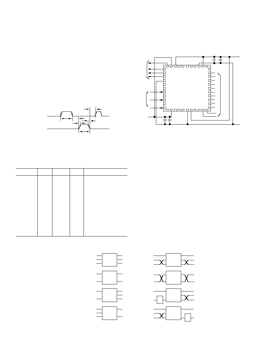
TIMING DIAGRAMS
Busy Output
The state of converter is indicated by the state of the BUSY out-
put (Pin 44). The BUSY output will go HI at the negative edge
of the STROBE input. This is used to synchronize digital input
data and load the digital angular rotation information into the
device counter. The BUSY output will remain HI for 2
µ
s, and
go LO until the next strobe negative edge occurs.
Strobe Input
The width of the positive STROBE pulse should be at least
100 ns, in order to successfully start the conversion. The maxi-
mum frequency of STROBE input is 366 kHz, i.e., there should
be at least 2.73
µ
s from the negative edge of one STROBE pulse
to the next rising edge. This is illustrated by the following tim-
ing diagram and table.
t
1
t
2
t
3
t
4
STROBE
BUSY
t
f
t
r
Figure 7. AD2S100 Timing Diagram
Note: Digital data should be stable 25 ns before and after posi-
tive strobe edge.
Table II. AD2S100 Timing Table
Parameter
Min
Typ
Max
Condition
t
1
100 ns
STROBE Pulse Width
t
2
30 ns
STROBE
to BUSY
t
3
1.7
µ
s
2.5
µ
s
BUSY Pulse Width
t
4
100 ns
BUSY
to STROBE
t
r
20 ns
BUSY Pulse Rise Time
with No Load
150 ns
BUSY Pulse Rise Time
with 68 pF Load
t
f
10 ns
BUSY Pulse Fall Time
with No Load
120 ns
BUSY Pulse Fall Time
with 68 pF Load
TYPICAL CIRCUIT CONFIGURATION
Figure 8 shows a typical circuit configuration for the AD2S100
in a three phase, nominal level input mode (MODE2).
THREE PHASE INPUT
AD2S100
TOP VIEW
1
41
38
30
27
23
12
16
DIGITAL ANGLE INPUT
LSB
SIN
COS
10µF
100nF
10µF
100nF
5V
+5V
GND
TWO/THREE PHASE
OUTPUT
STROBE
BUSY
HPOP
HPFILT
HPREF
MSB
PH/OP1
PH/OP3
PH/OP2
AGND
PH/IP4
PH/IP3
PH/IP2
PH/IP1
34
Figure 8. Typical Circuit Configuration
APPLICATIONS
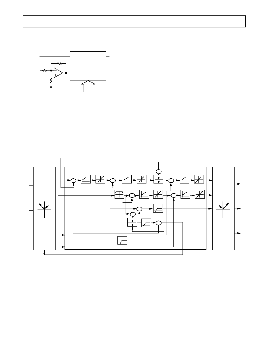
Forward and ReverseTransformation
The AD2S100 can perform both forward and reverse transfor-
mations. The section "Theory of Operation" explains how the
chip operates with the core operator e
+j
, which performs a for-
ward transformation. The reverse transformation, e
j
, is not
mentioned in the above sections of the data sheet simply to
avoid the confusion in the functionality and pinout. However,
the reverse transformation is very useful in many different appli-
cations, and the AD2S100 can be easily configured in a reverse
transformation configuration. Figure 9 shows four different
phase input/output connections for AD2S100 reverse transfor-
mation operation.
1
3 PHASE 3 PHASE
e
j
1
e
+j
e
+j
e
+j
e
+j
2 PHASE 2 PHASE
2 PHASE 3 PHASE
3 PHASE 2 PHASE
FORWARD
TRANSFORMATION
AD2S100
REVERSE
TRANSFORMATION
AD2S100
Cos
Sin
Cos(
+
)
Cos(
+
+ 120
°
)
Cos(
+
+ 240
°
)
Cos(
+ 120
°
)
Cos(
+ 240
°
)
Cos
Sin
Cos
Cos
Cos(
+ 120
°
)
Cos(
+ 240
°
)
Cos(
+
)
Sin(
+
)
Cos(
+
)
Cos(
+
+ 120
°
)
Cos(
+
+ 240
°
)
Cos(
+
)
Sin(
+
)
Cos
Cos(
+ 120
°
)
Cos(
+ 240
°
)
Cos(
)
Cos(
+ 120
°
)
Cos(
+ 240
°
)
Cos(
)
Cos(
+ 120
°
)
Cos(
+ 240
°
)
Cos
Sin
Cos(
)
Sin(
)
Cos
Sin
Cos
Cos(
+ 120
°
)
Cos(
+ 240
°
)
Cos(
)
Sin(
)
e
j
e
j
e
j
Figure 9. Reverse Transformation Connections
AD2S100
REV. A
9
In Figure 9, "1" operator performs a 180
°
phase shift opera-
tion. It can be illustrated by a 2-phase-to-3-phase reverse trans-
formation. An example is shown in Figure 10.
AD2S100
PH/IP1 (Cos
)
PH/OP1
Cos(
+
)
PH/OP3
Cos(
+ 240
°
+
)
PH/IP4 (Sin
)
PH/OP2
Cos(
+ 120
°
+
)
Cos
Sin
Cos(
)
Cos(
+ 240
°
)
Cos(
+ 120
°
)
R
R
R
2
Figure 10. Two-Phase to Three-Phase Reverse
Transformation
Field Oriented Control of AC Induction Machine in a Rotor
Flux Frame
The architecture shown in Figure 11 identifies a simplified
scheme where the AD2S100 permits the DSP computing core
to execute the motor control in what is normally termed the
rotor reference frame. This reference frame actually operates in
synchronism with the rotor of a motor. This has significant
benefits regarding motor control efficiency and economics. The
calculating power required in the rotor reference frame is signifi-
cantly reduced because the currents and flux are rotating at the
slip frequency. This permits calculations to be carried out in
time frames of, 100
µ
s, or under by a fixed-point DSP. Bench-
mark timing in this type of architecture can attain floating-point
speed processing with a fixed-point processor. Perhaps the larg-
est advantage is in the ease with which the rotor flux position
can be obtained. A large amount of computation time is, there-
fore, removed by the AD2S100 vector processors due to the
split architecture shown in Figure 11. Motor control systems
employing one DSP to carry out the cartesian to polar transfor-
mations required for vector control are, therefore, tasked with
additional duties due to the fact that they normally operate in
the flux reference frame.
The robustness of the control system can also be increased by
carrying out the control in the rotor reference frame. This is
achieved through the ability to increase and improve both the
algorithm quality in nonlinear calculations attributed to magne-
tizing inductance and rotor time constant for example. An
increase in sampling time can also be concluded with this archi-
tecture by avoiding the additional computing associated with
number truncation and rounding errors which reduce the signal-
to-noise rejection ratio.
is1
is2
is3
VECTOR
CO-PROCESSOR
REVERSE
ROTATION
AD2S100
SPEED
CONTROL
LIMIT
TORQUE
CONTROL
LIMIT
FIELD
WEAKENING
FORWARD
ROTATION
AD2S100
VECTOR
CO-PROCESSOR
V
qs'
V
ds'
'
Vs1
Vs2
Vs3
v
v
v
CONTROL SOFTWARE ADSP2101
POSITION
FEEDBACK
VELOCITY
FEEDBACK
POSITION
SET POINT
+
'
iqs
ids
'
+
+
+
+
imr'
iqs
1
2
imr
md'
iqs'
ids'
iqs
ids
Cm
i
mr
max
v
+
+
2
+
+
(a + jb)e'
j
'
(a + jb)e
j
Tr
Figure 11. Rotor Reference Frame Architecture
AD2S100
REV. A
10
SIMPLE SLIP CONTROL
In an adjustable-frequency drive, the control strategy must en-
sure that motor operation is restricted to low slip frequencies,
resulting in stable operation with a high power factor and a high
torque per stator ampere. Figure 12 shows the block diagram of
simple slip control using the AD2S100. Here, the slip frequency
command
2
and the current amplitude command are sent to
the microprocessor to generate two orthogonal signals, |I| Sin
and |I| Cos
here (
=
2
.) With the actual shaft position angle,
, (resolver-to-digital converter) and the orthogonal signals from
AC
INDUCTION
MTR
PWM
+
INVERTER
AD2S100
µPROC
AD2S80A RDC
(I) SET
SLIP
FREQ
I Sin
I Cos
Ia
Ib
Ic
RESOLVER
2
=
d
dt
Figure 12. Slip Control of AC Induction Motor with
AD2S100
the
µ
P, the AD2S100 generates the inverter frequency and am-
plitude command into a three-phase format. The three-phase
sine wave reference currents are reproduced in the stator phases.
For general applications, both the steady-state and dynamic per-
formance of this simple control scheme is satisfactory. For de-
tailed information about this application, please refer to the
bibliography at the end of the data sheet.
ADVANCED PMSM SERVO CONTROL
Electronically commutated permanent magnet synchronous
motors (PMSM) are used in high performance drives for
machine tools and robotics. When a field orientated control
scheme is deployed, the resulting brushless drive has all the
properties required for servo applications in machine tool fed
drives, industrial robots, and spindle drives. These properties
include large torque/inertia ratio, a high peak torque capability
for fast acceleration and deceleration with high torsional stiff-
ness at standstill.
Figure 13 shows the AD2S100 configured for both forward and
reverse transformations. This architecture concludes both flux
and torque current components independently. The additional
control of Vd (flux component) allows for the implementation
of field weakening schemes and maintenance of power factor.
2/3
3/2
PMSM
INV +
PWM
AD2S100
AD2S100
AD2S82
+
+
+
PI
ref
Id
Iq
Idref
Iqref
Va
Vc
Vb
Vq
Vd
PI
PI
e
+j
e
j
Figure 13. PMSM Servo Control Using AD2S100
For more detailed information, please refer to the application
note "Vector Control Using a Single Vector Rotation Semicon-
ductor for Induction and Permanent Magnet Motors."
MOTION CONTROL DSP COPROCESSOR
AC induction motors are superior to dc motors with respect to
size/power ratio, weight, rotor inertia, maximum rotating veloc-
ity, efficiency and cost for motor ratings greater than 5 HP.
However, because of nonlinear and the highly interactive multi-
variable control structure, ac induction motors have been con-
sidered difficult to control in applications demanding variable
speed and torque.
Field orientated control theory and practice, under development
since 1975, has offered the same level of control enjoyed by tra-
ditional dc machines. Practical implementation of these algo-
rithms involves the use of DSP and microprocessor based
architectures. The AD2S100 removes the needs for software
implementation of the rotor-to-stator and stator-to-rotor trans-
formations in the DSP or
µ
P. The reduction in throughput
times from typically 100
µ
s (
µ
P) and 40
µ
s (DSP) to 2
µ
s in-
creases system bandwidths while also allowing additional fea-
tures to be added to the CPU. The combination of the fixed
point ADSP-2101 and the AD2S100, the "advanced motion
control engine" shown in Figure 14, enables bandwidths previ-
ously attainable only through the use of floating point devices.
For more detailed information on the AD2S100 vector control
application and on this advanced motion control engine, please
refer to application notes "Vector Control Using a Single Vector
Rotation Semiconductor for Induction and Permanent Magnet
Motors."
MEASUREMENT OF HARMONICS
Three-phase ac power systems are widely used in power genera-
tion, transmission and electric drive. The quality of the electric-
ity supply is affected by harmonics injected into the power main.
In inverter fed ac machines, fluxes and currents of various fre-
quencies are produced. Predominantly in ac machines the 5th
and 7th harmonics are the most damaging; their reaction with
the fundamental flux component produces 6th harmonic torque
pulsations. The subsequent pulsating torque output may result
in uneven motion of the motor, especially at low speeds.
The AD2S100 can be used to monitor and detect the presence
and magnitude of a particular harmonic on a three-phase line.
Figure 15 shows the implementation of such a scheme using the
AD2S100. Note, the actual line voltages will have to be scaled
before applying to the three-phase input of the AD2S100.
Selecting a harmonic is achieved by synchronizing the rotational
frequency of the park digital input,
, with the frequency of the
fundamental flux component and the integer harmonic selected.
The update rate, r, of the counters is determined by:
r
=
4096
n
×
2
Here, r = input clock pulse rate (pulses/second);
n = the order of harmonics to be measured;
= fundamental angular frequency of the ac signal.
AD2S100
REV. A
11
VECTOR
COPROCESSOR
AD2S100
ADC
HOST COMPUTER
ADSP-2101/
ADSP-2105
DAC
AD2S80A
R/D
CONVERTER
AD7874
DAC-8412
VECTOR
COPROCESSOR
AD2S100
ia, ib, ic
INDUCTION
MOTOR
INV
+
PWM
Figure 14. Advanced Motion Control Engine
The magnitude of the n-th harmonic as well as the fundamental
component in the power line is represented by the output of the
low-pass filter, a
k
. In concert with magnitude of the harmonic
the AD2S100 homopolar output will indicate whether the
three phases are balanced or not. For more details about this
application, refer to the related application note listed in the
bibliography.
LOW PASS
FILTER
e
j
PARK
TRANSFORMATION
12-BIT UP/DOWN
COUNTER
AD2S100
a
k
HOMOPOLAR
OUTPUT
PULSE INPUTS
DIRECTION
Va
Vb
Vc
TWO-TO-THREE
CLARK
TRANSFORMATION
Vd
Vq
Vd
1
Vq
1
Figure 15. Harmonics Measurement Using AD2S100
MULTIPLE POLE MOTORS
For multi-pole motor applications where a single speed resolver
is used, the AD2S100 input has to be configured to match the
electrical cycle of the resolver with the phasing of the motor
windings. The input to the AD2S100 is the output of a resolver-
to-digital converter, e.g., AD2S80A series. The parallel output
of the converter needs to be multiplied by 2
n1
, where
n = the number of pole parts of the motor. In practice this is
implemented by shifting the parallel output of the converter left
relative to the number of pole pairs.
Figure 16 shows the generic configuration of the AD2S80A with
the AD2S100 for a motor with n pole pairs. The MSB of the
AD2S100 is connected to MSB-(n-1) bit of the AD2S80A digi-
tal output, MSB-1 bit to MSB-(n-2) bit, . . ., LSB bit to LSB
bit of AD2S80A, etc.
MSB
MSB-1
.
.
.
MSB (n1)
.
.
.
LSB + (n1)
MSB
MSB-1
MSB-2
.
.
.
.
.
.
.
LSB
.
.
.
.
AD2S80A
AD2S100
12,14 OR 16-BIT RESOLUTION MODE
n = POLES
Figure 16. A General Consideration in Connecting R/D
Converter and AD2S100 for Multiple Pole Motors
Figure 17 shows the AD2S80A configured for use with a four
pole motor, where n = 2. Using the formula described the MSB
is shifted left once
AD2S80A
AD2S100
BIT1
BIT2
.
.
.
.
.
.
BIT13
BIT14
MSB
MSB-1
.
.
.
.
.
.
.
LSB
(MSB)
(LSB)
14-BIT RESOLUTION MODE
.
.
.
.
.
.
Figure 17. Connecting of R/D Converter AD2S80A and
AD2S100 for Four-Pole Motor Application
AD2S100
REV. A
12
DIGITAL-TO-RESOLVER AND SYNCHRO CONVERSION
The AD2S100 can be configured for use as a 12-bit digital-to-
resolver (DRC) or synchro converter (DSC). DRCs and DSCs
are used to simulate the outputs of a resolver or a synchro. The
simulated outputs are represented by the transforms outlined
below.
Resolver Outputs
Asin
t.cos
Asin
t.sin
Synchro Outputs
Asin
t.sin
Asin
t.
sin (
+ 120
°
)
Asin
t.
sin (
+ 240
°
)
where:
Asin
t = fixed ac reference
= digital input angle, i.e., shaft position
The waveforms are shown in Figures 18 and 19.
360
°
90
°
R2 TO R4
(REF)
0
°
S3 TO S1
(SIN)
S2 TO S4
(COS)
270
°
180
°
Figure 18. Electrical Representation and Typical Resolver
Signals
360
°
90
°
0
°
S1 TO S2
270
°
180
°
S2 TO S3
S3 TO S1
R1 TO R2
Figure 19. Electrical Representation and Typical Synchro
Signals
Configuring the AD2S100 for DRC and DSC operation is done
by the following.
DRC--Must Select Mode 1
Inputs
PH/IP4
Pin 11
AGND
PH/IP1
Pin 1
Reference Asin
t
Outputs
PH/OP1
Pin 7
Asin
t Cos
PH/OP4
Pin 6
Asin
t Sin
DSC--Must Select Mode 1
Inputs
PH/IP4
Pin 11
Reference Asin
t
PH/IP1
Pin 17
AGND
Outputs
PH/OP1
Pin 7
Asin
t Sin
PH/OP2
Pin 9
Asin
t Sin (
+ 120
°
)
PH/OP3
Pin 8
Asin
t Sin (
+ 240
°
)
NOTES
1. Valid information is only available after the strobe pulse and BUSY go low.
For more information on DRCs see the AD2S65/AD2S66 data sheet.
2. To correct for inverse phasing of the DSC outputs the reference should be
inverted, or the MSB can be inverted.
APPLICATION NOTES LIST
1. "Vector Control Using a Single Vector Rotation Semiconduc-
tor for Induction and Permanent Magnet Motors," by F. P.
Flett, Analog Devices.
2. "Gamana DSP Vector Coprocessor for Brushless Motor
Control," by Analog Devices and Infosys Manufacturing
System.
3. "Silicon Control Algorithms for Brushless Permanent Magnet
Synchronous Machines," by F. P. Flett.
4. "Single Chip Vector Rotation Blocks and Induction Motor
Field Oriented Control," by A. P. M. Van den Bossche and
P. J. M. Coussens.
5. "Three Phase Measurements with Vector Rotation Blocks in
Mains and Motion Control," P. J. M. Coussens, et al.
6. "Digital to Synchro and Resolver Conversion with the AC
Vector Processor AD2S100," by Dennis Fu.
7. "Experiment with the AD2S100 Evaluation Board," by
Dennis Fu.
C1938187/94
PRINTED IN U.S.A
.
OUTLINE DIMENSIONS
Dimensions shown in inches and (mm).
44-Lead Plastic Leaded Chip Carrier (P-44A)
0.032 (0.81)
0.026 (0.66)
0.021 (0.53)
0.013 (0.33)
0.056 (1.42)
0.042 (1.07)
0.025 (0.63)
0.015 (0.38)
0.180 (4.57)
0.165 (4.19)
0.63 (16.00)
0.59 (14.99)
0.110 (2.79)
0.085 (2.16)
0.040 (1.01)
0.025 (0.64)
0.050
(1.27)
BSC
0.656 (16.66)
0.650 (16.51)
SQ
0.695 (17.65)
0.685 (17.40)
SQ
0.048 (1.21)
0.042 (1.07)
0.048 (1.21)
0.042 (1.07)
40
6
TOP VIEW
39
29
18
17
PIN 1
IDENTIFIER
7
28
0.020
(0.50)
R
Document Outline
- Specifications
- Pinout
- Package drawings
- Ordering Guide
- Features
- Applications
- Product Description
- Absolute Maximum Ratings
- Functional Block Diagram
- Pin Function Description
- Circuit Description
- PRODUCT HIGHLIGHTS
- RECOMMENDED OPERATING CONDITIONS
- CONVERTER OPERATION
- CONNECTING THE CONVERTER
- ANALOG SIGNAL INPUT AND OUTPUT CONNECTIONS
- HOMOPOLAR OUTPUT
- TIMING DIAGRAMS
- TYPICAL CIRCUIT CONFIGURATION
- SIMPLE SLIP CONTROL
- ADVANCED PMSM SERVO CONTROL
- MOTION CONTROL DSP COPROCESSOR
- MEASUREMENT OF HARMONICS
- MULTIPLE POLE MOTORS
- DIGITAL-TO-RESOLVER AND SYNCHRO CONVERSION
- APPLICATION NOTES LIST
- DIAGRAMS
- Vector Rotation Operation
- Converter Operation Diagram
- Power Supply Connection
- The Equivalent Homopolar Reference Input Circuitry
- Homopolar Output Connections
- Timing Diagram
- Reverse Transformation Connections
- Two-Phase to Three-Phase Reverse Transformation
- Rotor Reference Frame Architecture
- Slip Control of AC Induction Motor
- PMSM Servo Control Using AD2S100
- Advanced Motion Control Engine
- Harmonics Measurement Using AD2S100
- A General Consideration in Connecting R/D Converter and AD2S100 for Multiple Pole Motors
- Connecting of R/D Converter AD2S80A and AD2S100 for Four Pole Motor Application