 | ÐлекÑÑоннÑй компоненÑ: AD2S105AP | СкаÑаÑÑ:  PDF PDF  ZIP ZIP |
Äîêóìåíòàöèÿ è îïèñàíèÿ www.docs.chipfind.ru
One Technology Way, P.O. Box 9106, Norwood. MA 02062-9106, U.S.A.
Tel: 617/329-4700
Fax: 617/326-8703
REV. 0
Information furnished by Analog Devices is believed to be accurate and
reliable. However, no responsibility is assumed by Analog Devices for its
use, nor for any infringements of patents or other rights of third parties
which may result from its use. No license is granted by implication or
otherwise under any patent or patent rights of Analog Devices.
a
FEATURES
Current Conditioning
Complete Vector Transformation on Silicon
Three-Phase 120
°
and Orthogonal 90
°
Signal
Transformation
Three-Phase Balance DiagnosticHomopolar Output
DQ Manipulation
Real-Time Filtering
APPLICATIONS
AC Induction Motor Control
Spindle Drive Control
Pump Drive Control
Compressor Drive Control and Diagnostics
Harmonic Measurement
Frequency Analysis
Three-Phase Power Measurement
Three-Phase
Current Conditioner
AD2S105
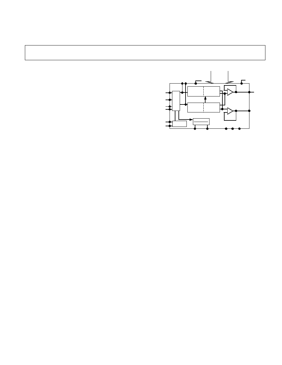
FUNCTIONAL BLOCK DIAGRAM
GENERAL DESCRIPTION
The AD2S105 performs the vector rotation of three-phase 120
degree or two-phase 90 degree sine and cosine signals by trans-
ferring these inputs into a new reference frame which is controlled
by the digital input angle
. Two transforms are included in the
AD2S105. The first is the Clarke transform which computes
the sine and cosine orthogonal components of a three-phase in-
put. These signals represent real and imaginary components
which then form the input to the Park transform. The Park
transform relates the angle of the input signals to a reference
frame controlled by the digital input port. The digital input
port on the AD2S105 is a 12-bit/parallel natural binary port.
If the input signals are represented by Vds and Vqs, respectively,
where Vds and Vqs are the real and imaginary components, then
the transformation can be described as follows:
Vds' = Vds Cos
Vqs Sin
Vqs' = Vds Sin
+ Vqs Cos
Where Vds' and Vqs' are the output of the Park transform
and Sin
, and Cos
are the trigonometric values internally cal-
culated by the AD2S105 from the binary digital data
.
The input section of the device can be configured to accept
either three-phase inputs, two-phase inputs of a three-phase
system, or two 90 degree input signals. The homopolar output
indicates an imbalance of a three-phase input only at a user-
specified level.
The digital input section will accept a resolution of up to 12 bits.
An input data strobe signal is required to synchronize the position
data and load this information into the device counters.
I
S1
Vds
Vqs
SECTOR
MULTIPLIER
SINE AND
COSINE
MULTIPLIER
INPUT
DATA
STROBE
HOMOPOLAR
OUTPUT
HOMOPOLAR
REFERENCE
+5V GND 5V
POSITION
PARALLEL
DATA
12 BITS
3
-2
Cos (
+
120
°)
Cos (
+
240
°)
Sin
Cos
Cos
Sin
Cos
+
CONV1
CONV2
DECODE
BUSY
Vds'
Vqs'
Sin
+
SECTOR
MULTIPLIER
SINE AND
COSINE
MULTIPLIER
Ia + Ib + Ic
3
I
S2
I
S3
A two-phase rotated output facilitates the implementation of
multiple rotation blocks.
The AD2S105 is fabricated on LC
2
MOS and operates on
±
5 volt power supplies.
PRODUCT HIGHLIGHTS
Current Conditioning
The AD2S105 transforms the analog stator current signals (I
s1
,
I
s
2
, I
s
3
) using the digital angular signal (reference frame) into dc
values which represent direct current (I
ds
) and quadrature cur-
rent (I
qs
). This transformation of the ac signals into dc values
simplifies the design of the analog-to-digital (A/D) conversion
scheme. The A/D conversion scheme is simplified as the band-
width sampling issues inherent in ac signal processing are
avoided and in most drive designs, simultaneous sampling of the
stator currents may not be necessary.
Hardware Peripheral for Standard Microcontroller and DSP
Systems
The AD2S105 off-loads the time consuming Cartesian transfor-
mations from digital processors and benchmarks show a signifi-
cant speed improvement over single processor designs. AD2S105
transformation time = 2
µ
s.
Field Oriented Control of AC Motors
The AD2S105 accommodates all the necessary functions to pro-
vide a hardware solution for current conditioning in variable
speed control of ac synchronous and asynchronous motors.
Three-Phase Imbalance Detection
The AD2S105 can be used to sense imbalances in a three-phase
system via the homopolar output.

AD2S105SPECIFICATIONS
Parameter
Min
Typ
Max
Units
Conditions
SIGNAL INPUTS
PH/IP1, 2, 3, 4 Voltage Level
±
2.8
±
3.3
V p-p
DC to 50 kHz
PH/IPH1, 2, 3 Voltage Level
±
4.25
V p-p
DC to 50 kHz
Input Impedance
PH/IP1, 2, 3
7.5
10
k
PH/IPH1, 2, 3
13.5
18
k
PH/IP1, 4
1
M
Mode 1 Only (2 Phase)
Sin & Cos
Gain
PH/IP1, 2, 3, 4
0.95
1
1.05
PH/IPH1, 2, 3
0.56
VECTOR PERFORMANCE
3-Phase Input-Output
Radius Error (Any Phase)
±
0.4
±
1
%
DC to 600 Hz
Angular Error
1, 2
PH/IP
15
30
arc min
DC to 600 Hz
PH/IPH
30
arc min
DC to 600 Hz
Differential Nonlinearity
±
1
LSB
Full Power Bandwidth
50
kHz
Small Signal Bandwidth
200
kHz
ANALOG SIGNAL OUTPUTS
PH/OP1, 4
PH/IP, PH/IPH INPUTS
Output Voltage
3
±
2.8
±
3.3
V p-p
DC to 50 kHz
Offset Voltage
2
10
mV
Inputs = 0 V
Slew Rate
2
V/
µ
s
Small Signal Step Response
1
µ
s
1
°
Input to Settle to
±
1 LSB (Input to Output)
Output Impedance
15
Output Drive Current
3.0
4.0
mA
Outputs to AGND
Resistive Load
2
k
Capacitive Load
50
pF
STROBE
Write
100
ns
Positive Pulse
Max Update Rate
366
kHz
BUSY
Pulse Width
1.7
2.5
µ
s
Conversion in Process
V
OH
4
V dc
I
OH
= 0.5 mA
V
OL
1
V dc
I
OL
= 0.5 mA
DIGITAL INPUTS
DB1DB12
V
IH
3.5
V dc
V
IL
1.5
V dc
Input Current, I
IN
±
10
µ
A
Input Capacitance, C
IN
10
pF
CONV MODE
(CONV1, CONV2)
V
IH
3.5
V dc
V
IL
1.5
V dc
Input Current
100
µ
A
Internal 50 k
Input Capacitance
10
pF
Pull-Up Resistor
REV. 0
2
(V
DD
= +5 V
±
5%; V
SS
= 5 V
±
5% AGND = DGND = O V;
T
A
= 40
°
C to +85
°
C, unless otherwise noted)

Parameter
Min
Typ
Max
Units
Conditions
HOMOPOLAR OUTPUT
HPOPOUTPUT
V
OH
4
V dc
I
OH
= 0.5 mA
V
OL
1
V dc
I
OL
= 0.5 mA
HPREFREFERENCE
0.5
V dc
Homopolar Output-Internal
I
SOURCE
= 25
µ
A and 20 k
to AGND
POWER SUPPLY
V
DD
4.75
5
5.25
V dc
V
SS
5.25
5
4.75
V dc
I
DD
4
10
mA
Quiescent Current
I
SS
4
10
mA
Quiescent Current
AD2S105
REV. 0
3
NOTES
1
Angular accuracy includes offset and gain errors, measured with a stationary digital input and maximum analog frequency inputs.
2
The angular error does not include the additional error caused by the phase delay as a function of input frequency. For example, if f
INPUT
= 600 Hz, the contribution
to the error due to phase delay is: 650 ns
×
f
INPUT
×
60
×
360 = 8.4 arc minutes.
3
Output subject to input voltage and gain.
Specifications subject to change without notice.
WARNING!
ESD SENSITIVE DEVICE
CAUTION
ESD (electrostatic discharge) sensitive device. Electrostatic charges as high as 4000 V readily
accumulate on the human body and test equipment and can discharge without detection.
Although the AD2S105 features proprietary ESD protection circuitry, permanent damage may
occur on devices subjected to high energy electrostatic discharges. Therefore, proper ESD
precautions are recommended to avoid performance degradation or loss of functionality.
RECOMMENDED OPERATING CONDITIONS
Power Supply Voltage (+V
DD
, V
SS
) . . . . . . . . .
±
5 V dc
±
5%
Analog Input Voltage (PH/IP1, 2, 3, 4) . . . . . . 2 V rms
±
10%
Analog Input Voltage (PH/IPH1, 2, 3) . . . . . . 3 V rms
±
10%
Ambient Operating Temperature Range
Industrial (AP) . . . . . . . . . . . . . . . . . . . . . . . 40
°
C to +85
°
C
ABSOLUTE MAXIMUM RATINGS
(T
A
= +25
°
C)
V
DD
to AGND . . . . . . . . . . . . . . . . . . . . . . . 0.3 V to +7 V dc
V
SS
to AGND . . . . . . . . . . . . . . . . . . . . . . . +0.3 V to 7 V dc
AGND to DGND . . . . . . . . . . . . . . . . . . . . . . . . . . .
±
0.3 V dc
Analog Input Voltage to AGND . . . . . . . . . . . . . . . V
SS
to V
DD
Digital Input Voltage to DGND . . . . 0.3 V to V
DD
+ 0.3 V dc
Digital Output Voltage to DGND . . . . . . 0.3 V to V
DD
+ V dc
Analog Output Voltage to AGND
. . . . . . . . . . . . . . . . . . . . . . V
SS
0.3 V to V
DD
+ 0.3 V dc
Analog Output Load Condition (PH/OP1, 4
Sin
, Cos
) . . . . . . . . . . . . . . . . . . . . . . . . . . . . . . . . . . . . . . . 2
k
Power Dissipation . . . . . . . . . . . . . . . . . . . . . . . . . . . . 140 mW
Operating Temperature
Industrial (AP) . . . . . . . . . . . . . . . . . . . . . . . 40
°
C to +85
°
C
Storage Temperature . . . . . . . . . . . . . . . . . 65
°
C to +150
°
C
Lead Temperature (Soldering, 10 sec) . . . . . . . . . . . . . +300
°
C
CAUTION
1. Absolute Maximum Ratings are those values beyond which
damage to the device will occur.
2. Correct polarity voltages must be maintained on the +V
DD
and V
SS
pins
ORDERING GUIDE
Model
Temperature Range
Accuracy
Option*
AD2S105AP
40
°
C to +85
°
C
30 arc min
P-44A
*P = Plastic Leaded Chip Carrier.
AD2S105
REV. 0
4
PIN DESIGNATIONS
1, 2, 3
Pin
Mnemonic
Description
3
STROBE
Begin Conversion
4
V
DD
Positive Power Supply
5
V
SS
Negative Power Supply
6
PH/OP4
Sin (
+ )
7
PH/OP1
Cos (
+ )
10
AGND
Analog Ground
11
PH/IP4
Sin
Input
12
PH/IPH3
High Level Cos
(
+ 240
°
) Input
13
PH/IP3
Cos (
+ 240
°
) Input
14
PH/IPH2
High Level Cos
(
+ 120
°
) Input
15
PH/IP2
Cos (
+ 120
°
) Input
16
PH/IPH1
High Level Cos
Input
17
PH/IP1
Cos
()
Input
19
V
SS
Negative Power Supply
20
HPREF
Homopolar Reference
21
HPOP
Homopolar Output
22
HPFILT
Homopolar Filter
23
CONV1
Select Analog Input
Format
24
CONV2
Select Analog Input
Format
25
COS
Cos Output
26
SIN
Sin Output
2738
DB12 to DB1
(DB1 = MSB, DB12 =
LSB Parallel Input Data)
41
V
DD
Positive Power Supply
42
DGND
Digital Ground
44
BUSY
Internal Logic Setup
Time
NOTES
1
90
°
orthogonal signals = Sin
, Cos
(Resolver) = PH/IP4 and PH/IP1.
2
Three phase, 120
°
, three-wire signals = Cos
, Cos (
+ 120
°
), Cos (
+ 240
°
).
= PH/IP1, PH/IP2, PH/IP3
High Level = PH/IPH1, PH/IPH2, PH/IPH3.
3
Three Phase, 120
°
, two-wire signals = Cos (
+ 120
°
), Cos (
+ 240
°
) =
PH/IP2, PH/IP3.
In all cases where any of the input Pins 11 through 17 are not used, they must
be left unconnected.
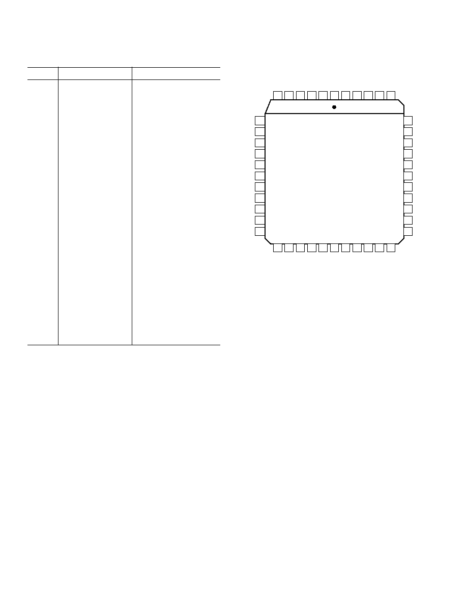
PIN CONFIGURATION
6
5
4
3
2
1
44
43
42
41
40
18
19
20
21
22
23
24
25
26
27
28
29
30
31
32
33
34
35
36
37
38
39
V
SS
V
DD
STROBE
NC
NC
BUSY
DGND
V
DD
NC
NC
V
SS
HPREF
HPOP
CONV1
CONV2
COS
DB12
HPFILT
DB11
NC = NO CONNECT.
TOP VIEW
(NOT TO SCALE)
AD2S105
PH/OP4
NC
SIN
7
8
11
12
13
14
15
16
17
9
10
NC
DB1
DB2
DB3
DB4
DB5
DB6
DB7
DB8
DB9
DB10
PH/OP1
NC
NC
AGND
PH/IP4
PH/IPH3
PH/IP3
PH/IPH2
PH/IP2
PH/IPH1
PH/IP1
AD2S105
REV. 0
5
THEORY OF OPERATION
A fundamental requirement for high quality induction motor
drives is that the magnitude and position of the rotating air-gap
rotor flux be known. This is normally carried out by measuring
the rotor position via a position sensor and establishing a rotor
oriented reference frame.
To generate a flux component in the rotor, stator current is ap-
plied. A build-up of rotor flux is concluded which must be
maintained by controlling the stator current, i
ds
, parallel to the
rotor flux. The rotor flux current component is the magnetizing
current, i
mr
.
Torque is generated by applying a current component which is
perpendicular to the magnetizing current. This current is nor-
mally called the torque generating current, i
qs
.
To orient and control both the torque and flux stator current
vectors, a coordinate transformation is carried out to establish a
new reference frame related to the rotor. This complex calcula-
tion is carried out by the AD2S105.
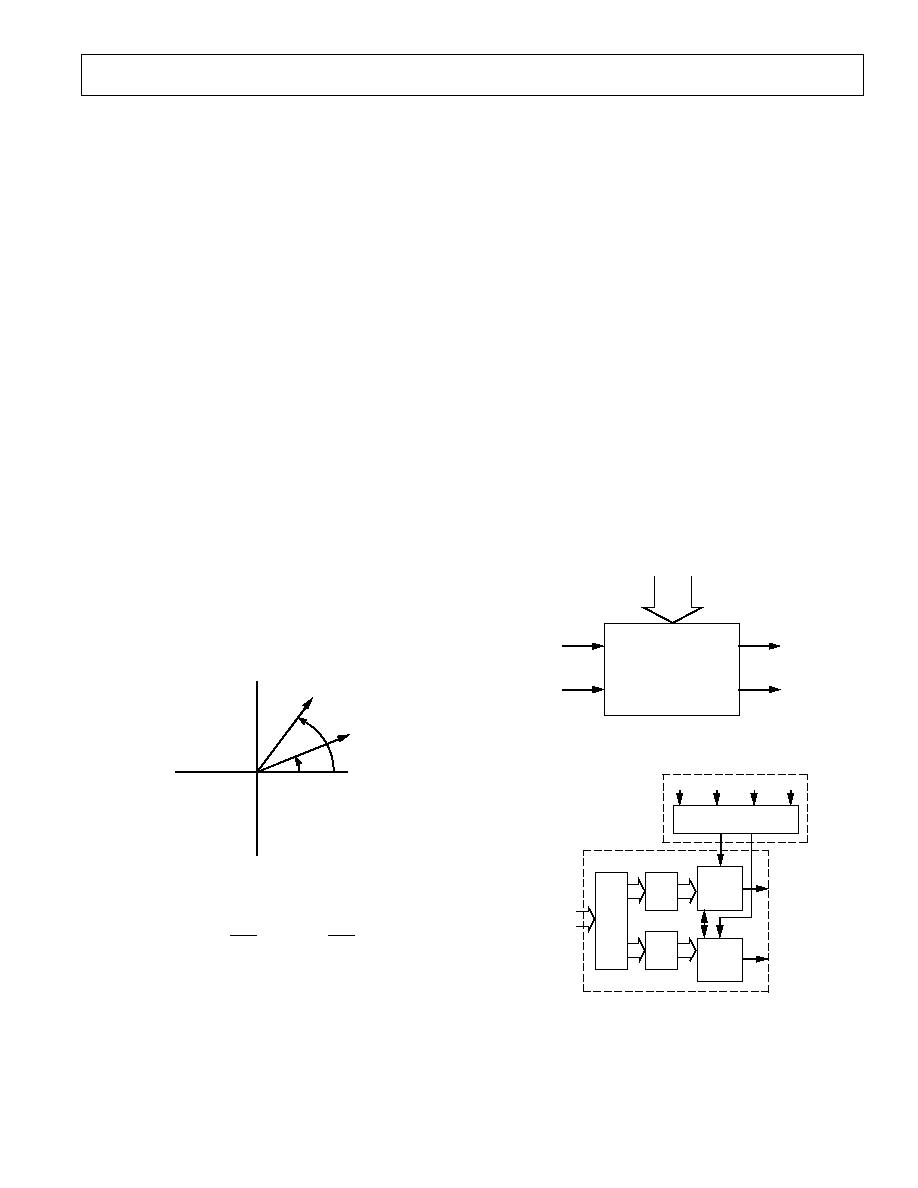
To expand upon the vector operator a description of a single
vector rotation is of assistance. If it is considered that the
moduli of a vector is OP and that through the movement of ro-
tor position by , we require the new position of this vector it
can be deduced as follows:
Let original vector OP = A (Cos + jSIN ) where A is a
constant;
if
OQ = OP e
j
(1)
and: e
j
= Cos + jSin
OQ = A (Cos ( +
) + jSin ( + ))
= A [Cos Cos
Sin Sin
+ jSin Cos
+ jCos Sin
]
= A [(Cos + jSin ) (Cos
+ jSin )]
(2)
+
Q
P
O
a
d
Figure 1. Vector Rotation in Polar Coordinate
The complex stator current vector can be represented as i
s
= i
as
+ ai
bs
+ a
2
i
cs
where a = e
j 2
3
and a
2
= e
j 4
3
. This can be re-
placed by rectangular coordinates as
i
s
= i
ds
+ ji
qs
(3)
In this equation i
ds
and i
qs
represent the equivalent of a two-
phase stator winding which establishes the same magnitude of
MMF in a three-phase system. These inputs can be seen after
the three-phase to two-phase transformation in the AD2S105
block diagram. Equation (3) therefore represents a three-phase
to two-phase conversion.
To relate these stator current to the reference frame the rotor
currents assume the same rectangular coordinates, but are now
rotated by the operator e
j
, where e
j
= Cos + jSin .
Here the term vector rotator comes into play where the stator
current vector can be represented in rotor-based coordinates or
vice versa.
The AD2S105 uses e
j
as the core operator. In terms of the
mathematical function, it rotates the orthogonal i
ds
and i
qs
com-
ponents as follows:
i
ds
' + ji
qs
' = (I
ds
+ jI
qs
) e
j
where i
ds
', i
qs
' = stator currents in the rotor reference frame. And
e
j
= Cos + jSin
= (I
ds
+ jI
qs
)(Cos + jSin )
The output from the AD2S105 takes the form of:
i
ds
' = I
ds
Cos I
qs
Sin
i
qs
' = I
ds
Sin + I
qs
Cos
The matrix equation is:
[
i
ds
'
]
=
[
Cos
Sin
] [
I
ds
]
i
qs
'
Sin
Cos
I
qs
and it is shown in Figure 2.
I
ds
I
qs
I
ds
'
I
qs
'
e
j
Figure 2. AD2S105 Vector Rotation Operation
DIGITAL
LATCH
3
TO 2
TRANSFORMATION
LATCH
LATCH
SINE AND
COSINE
MULTIPLIER
(DAC)
SINE AND
COSINE
MULTIPLIER
(DAC)
PARK
COS
COS
+ 120
°
COS
+ 240
°
SIN
INPUT CLARK
COS (
+ )
SIN (
+ )
Figure 3. Converter Operation Diagram
Document Outline
- Specifications
- Pinout
- Package drawings
- Ordering Guide
- Features
- Applications
- Product Description
- Absolute Maximum Ratings
- Functional Block Diagram
- Pin Function Description
- Circuit Description
- PRODUCT HIGHLIGHTS
- RECOMMENDED OPERATING CONDITIONS
- CONVERTER OPERATION
- CONNECTING THE CONVERTER
- ANALOG SIGNAL INPUT AND OUTPUT CONNECTIONS
- HOMOPOLAR OUTPUT
- TIMING DIAGRAMS
- TYPICAL CIRCUIT CONFIGURATION
- MEASUREMENT OF HARMONICS
- MULTIPLE POLE MOTORS
- APPLICATION NOTES LIST
- DIAGRAMS
- Vector Rotation Operation
- Converter Operation Diagram
- Power Supply Connection
- The Equivalent Homopolar Reference Input Circuitry
- Homopolar Output Connections
- Timing Diagram
- Forward and Reverse Transformation Connections
- Harmonics Measurement Using AD2S105
- Field Oriented Control of AC Induction Motors
- A General Consideration in Connecting R/D Converter and AD2S105 for Multiple Pole Motors
- Connecting of R/D Converter AD2S80A and AD2S105 for Four-Pole Motor Application