64-Position OTP Digital Potentiometer
AD5171
FEATURES
64 positions
OTP (one-time programmable)
1
set-and-forget resistance
setting--low cost alternative over EEMEM
Unlimited adjustments prior to OTP activation
5 k, 10 k, 50 k, 100 k end-to-end resistance
Low tempco 5 ppm/
o
C in potentiometer mode
Rev. PrC
Low tempco 35 ppm/∞C in rheostat mode
Compact standard SOT-23-8 package
Low power, I
DD
= 8 µA max
Fast settling time, t
s
= 5 µs typ in power-up
I
2
C compatible digital interface
Computer software replaces µc in factory programming
applications
Full read/write of wiper register
Extra I
2
C device address pin
Power-on preset to midscale
6 V one-time programming voltage
Low operating voltage, 2.7 V to 5.5 V
OTP validation check function
Automotive temperature range -40∞C to +125∞C
APPLICATIONS
Systems calibrations
Electronics level settings
Mechanical potentiometers and trimmersÆ replacements
Automotive electronics adjustments
Gain control and offset adjustments
Transducer circuits adjustments
Programmable filters up to 1.5 MHz BW
GENERAL DESCRIPTION
The AD5171 is a 64-position, one-time programmable (OTP)
digital potentiometer
2
, which employs fuse link technology to
achieve the memory retention of resistance setting function.
OTP is a cost-effective alternative over the EEMEM approach
for users who do not need to reprogram new memory setting in
the digital potentiometer. This device performs the same
electronic adjustment function like most mechanical trimmers
and variable resistors do. The AD5171 is programmed using a
2-wire I
2
C compatible digital control. It allows unlimited
adjustments before permanently setting the resistance value.
During the OTP activation, a permanent fuse blown command
is sent after the final value is determined; therefore freezing the
wiper position at a given setting (analogous to placing epoxy on
a mechanical trimmer). When this permanent setting is
achieved, the value will not change regardless of supply
variations or environmental stresses under normal operating
conditions. To verify the success of permanent programming,
Analog Devices patterned the OTP validation such that the fuse
status can be discerned from two validation bits in read mode.
For applications that program AD5171 in the factories, Analog
Devices offers a device programming software, which operates
across WindowsÆ 95 to XPÆ platforms including Windows NTÆ.
This software application effectively replaces the need for
external I
2
C controllers or host processors and therefore
significantly reduces users' development time.
An AD5171 evaluation kit is available, which includes the
software, connector, and cable that can be converted for the
factory programming applications.
The AD5171 is available in a compact SOT-23-8 package. All
parts are guaranteed to operate over the automotive
temperature range of -40∞C to +125∞C. Besides its unique OTP
feature, the AD5171 lends itself well to other general-purpose
digital potentiometer applications due to its temperature
performance, small form factor, and low cost.
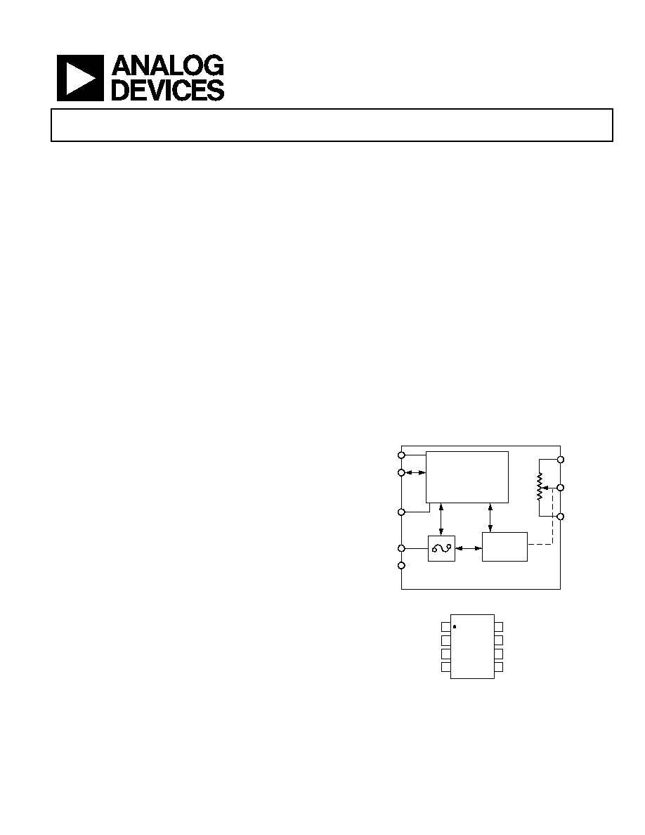
GND
I
2
C INTERFACE
AND
CONTROL LOGIC
A
W
B
WIPER
REGISTER
FUSE
LINK
V
DD
AD0
SDA
SCL
AD5171
03437-0-001
Figure 1.
Functional Block Diagram
TOP VIEW
(Not to Scale)
8
7
6
5
1
2
3
4
W
V
DD
GND
SCL
A
B
AD0
SDA
AD5171
03437-
0-
002
Figure 2. Pin Configuration
1
One-time programmable (OTP) - Unlimited adjustments before permanent
setting.
2
The terms digital potentiometer and RDAC are used interchangeably.
Information furnished by Analog Devices is believed to be accurate and reliable.
However, no responsibility is assumed by Analog Devices for its use, nor for any
infringements of patents or other rights of third parties that may result from its use.
Specifications subject to change without notice. No license is granted by implication
or otherwise under any patent or patent rights of Analog Devices. Trademarks and
registered trademarks are the property of their respective owners.
One Technology Way, P.O. Box 9106, Norwood, MA 02062-9106, U.S.A.
Tel: 781.329.4700
www.analog.com
Fax: 781.326.8703
© 2003 Analog Devices, Inc. All rights reserved.
Preliminary Technical Data

AD5171
TABLE OF CONTENTS
AD5171--Electrical Characteristics .............................................. 3
Absolute Maximum Ratings............................................................ 5
ESD Caution.................................................................................. 5
Pin Configuration and Functional Descriptions.......................... 6
Typical Performance Characteristics ............................................. 7
Theory of Operation ...................................................................... 11
One-Time Programming (OTP) .............................................. 11
Determining the Variable Resistance and Voltage ................. 11
Rheostat Mode Operation..................................................... 11
Potentiometer Mode Operation ........................................... 12
ESD Protection ........................................................................... 12
Terminal Voltage Operating Range.......................................... 13
Power-Up/Power-Down Sequences......................................... 13
Power Supply Considerations ................................................... 13
Controlling the AD5171 ............................................................ 14
Software Programming ......................................................... 14
I
2
C Controller Programming................................................ 15
Controlling Two Devices on One Bus ..................................... 16
Applications..................................................................................... 17
Programmable Voltage Reference (DAC) ............................... 17
Gain Control Compensation .................................................... 17
Programmable Voltage Source with Boosted Output............ 17
Level Shifting for Different Voltage Operation ...................... 17
Resistance Scaling ...................................................................... 17
Resolution Enhancement .......................................................... 18
RDAC Circuit Simulation Model ............................................. 18
AD5171 Evaluation Board ........................................................ 19
Outline Dimensions ....................................................................... 20
Ordering Guide .......................................................................... 20
REVISION HISTORY
Revision 0: Initial Version
Rev. PrC | Page 2 of 20
Preliminary Technical Data

AD5171
ELECTRICAL CHARACTERISTICS
Table 1. 5 k, 10 k, 50 k, and 100 k versions, V
DD
= 3 V to 5 V ± 10%, V
A
= V
DD
, V
B
= 0 V, -40∞C < T
A
< +125∞C,
unless otherwise noted.
Parameter Symbol
Conditions
Min
Typ
1
Max Unit
DC CHARACTERISTICS RHEOSTAT MODE
Resistor Differential Nonlinearity
2
R-DNL
R
WB
, V
A
= No Connect,
R
AB
= 10 k, 50 k, and 100
k
≠0.5 ±0.2 +0.5 LSB
R
WB
, V
A
= No Connect, R
AB
= 5
k
≠1 ±0.25
+1 LSB
Resistor Integral Nonlinearity
2
R-INL
R
WB
, V
A
= No Connect,
R
AB
= 10 k, 50 k, and 100 k
≠1 ±0.25
+1 LSB
R
WB
, V
A
= No Connect, R
AB
= 5
k
≠1.5 ±0.5 +1.5 LSB
Nominal Resistor Tolerance
3
R
AB
/R
AB
≠30
+30 %
Resistance Temperature Coefficient
(R
AB
/R
AB
)/T
35
ppm/∞C
Wiper Resistance
R
W
V
DD
= 5 V
60
115
DC CHARACTERISTICS POTENTIOMETER DIVIDER
MODE (Specifications apply to all RDACs)
Resolution N
6
Bits
Differential Nonlinearity
4
DNL
≠0.5
±0.1
+0.5
LSB
Integral Nonlinearity
4
INL
≠1
±0.2
+1
LSB
Voltage Divider Temperature Coefficient
(V
W
/V
W
)/T
Code = 0x20
5
ppm/∞C
Full-Scale Error
V
WFSE
Code = 0x3F
≠1.5
-0.5
+0
LSB
Zero-Scale Error
V
WZSE
Code = 0x00, R
AB
=10 k,
50 k, and 100 k
0 0.5
1.5 LSB
Code = 0x00, R
AB
= 5 k
0
2
LSB
RESISTOR TERMINALS
Voltage Range
5
V
A, B, W
With respect to GND
V
DD
V
Capacitance
6
A, B
C
A, B
f = 1 MHz, measured to GND,
Code = 0x20
25
pF
Capacitance
6
W
C
W
f = 1 MHz, measured to GND,
Code = 0x20
55
pF
Common-Mode Leakage
I
CM
V
A
= V
B
= V
DD
/2
1
nA
DIGITAL INPUTS
Input Logic High (SDA and SCL)
V
IH
0.7
V
DD
V
DD
+0.5 V
Input Logic Low (SDA and SCL)
V
IL
≠0.5
0.3V
DD
V
Input Logic High (AD0)
V
IH
V
DD
= 3 V
3.0
V
DD
V
Input Logic Low (AD0)
V
IL
V
DD
= 3 V
0
1.0
V
Input Current
I
IL
V
IN
= 0 V or 5 V
±1
µA
Input Capacitance
6
C
IL
3
pF
DIGITAL OUTPUTS
Output Logic Low (SDA)
V
OL
I
OL
= 6 mA
0.4
V
Three-State Leakage Current (SDA)
I
OZ
V
IN
= 0 V or 5 V
±1
µA
Output Capacitance
6
C
OZ
3
pF
POWER SUPPLIES
Power Supply Range
V
DD
2.7
5.5
V
OTP Power Supply
7
V
DD_OTP
T
A
= 25∞C
6
6.5
V
Supply Current
I
DD
V
IH
= 5 V or V
IL
= 0 V
4
8
µA
OTP Supply Current
8
I
DD_OTP
V
DD_OTP
= 6 V, T
A
= 25∞C
100
mA
Power Dissipation
9
P
DISS
V
IH
= 5 V or V
IL
= 0 V, V
DD
= 5 V
0.02
0.04
mW
Power Supply Sensitivity
PSSR
-0.025
+0.001
+0.025
%/%
Rev. PrC | Page 3 of 20
Preliminary Technical Data

AD5171
Parameter Symbol
Conditions
Min
Typ
1
Max Unit
DYNAMIC CHARACTERISTICS
6, 10, 11
Bandwidth ≠3 dB
BW_5k
R
AB
= 5 k, Code = 0x20
1500
kHz
BW_10k
R
AB
= 10 k, Code = 0x20
600
kHz
BW_50k
R
AB
= 50 k, Code = 0x20
110
kHz
BW_100k
R
AB
= 100 k, Code = 0x20
60
kHz
Total Harmonic Distortion
THD
V
A
=1 V rms, R
AB
= 10 k,
V
B
= 0 V D
C
, f = 1 kHz
0.05
%
Adjustment Settling Time
t
S1
V
A
= 5 V ± 1 LSB error band,
V
B
= 0, measured at V
W
5
µs
OTP Settling Time
12
t
S_OTP
V
A
= 5 V ± 1 LSB error band,
V
B
= 0, measured at V
W
400
ms
Power-up Settling Time--Post Fuses Blown
t
S2
V
A
= 5 V ±1 LSB error band,
V
B
= 0, measured at V
W
5
µs
Resistor Noise Voltage
e
N_WB
R
AB
= 5 k, f = 1 kHz,
Code = 0x20
8
nV/Hz
R
AB
= 10 k, f = 1 kHz,
Code = 0x20
12
nV/Hz
INTERFACE TIMING CHARACTERISTICS
(Applies to all parts
6,12
)
SCL Clock Frequency
f
SCL
400
kHz
t
BUF
Bus Free Time between Start and Stop
t
1
1.3
µs
t
HD;STA
Hold Time (Repeated Start)
t
2
After this period, the first
clock pulse is generated
0.6
µs
t
LOW
Low Period of SCL Clock
t
3
1.3
µs
t
HIGH
High Period of SCL Clock
t
4
0.6
50
µs
t
SU;STA
Setup Time for Start Condition
t
5
0.6
µs
t
HD;DAT
Data Hold Time
t
6
0.9
µs
t
SU;DAT
Data Setup Time
t
7
0.1
µs
t
F
Fall Time of Both SDA and SCL Signals
t
8
0.3
µs
t
R
Rise Time of Both SDA and SCL signals
t
9
0.3
µs
t
SU;STO
Setup Time for Stop Condition
t
10
0.6
µs
1
Typicals represent average readings at 25∞C and V
DD
= 5 V.
2
Resistor position nonlinearity error R-INL is the deviation from an ideal value measured between the maximum resistance and the minimum resistance wiper positions.
R-DNL measures the relative step change from ideal between successive tap positions. Parts are guaranteed monotonic.
3
V
AB
= V
DD
, Wiper (V
W
) = No connect.
4
INL and DNL are measured at V
W
with the RDAC configured as a potentiometer divider similar to a voltage output DAC. V
A
= V
DD
and V
B
= 0 V. DNL specification limits of
±1 LSB maximum are guaranteed monotonic operating conditions.
5
Resistor terminals A, B, W have no limitations on polarity with respect to each other.
6
Guaranteed by design and not subject to production test.
7
Different from operating power supply, power supply for OTP is used one-time only.
8
Different from operating current, supply current for OTP lasts approximately 400 ms for one-time needed only.
9
P
DISS
is calculated from (I
DD
◊ V
DD
). CMOS logic level inputs result in minimum power dissipation.
10
Bandwidth, noise, and settling time are dependent on the terminal resistance value chosen. The lowest R value results in the fastest settling time and highest
bandwidth. The highest R value result in the minimum overall power consumption.
11
All dynamic characteristics use V
DD
= 5 V.
12
Different from settling time after fuse is blown. The OTP settling time occurs once only.
SCL
SDA
t
1
t
2
t
3
t
8
t
8
t
9
t
4
t
5
t
9
t
7
t
6
t
10
P
P
S
03437-0-024
Figure 3. Interface Timing Diagram
Rev. PrC | Page 4 of 20
Preliminary Technical Data

AD5171
ABSOLUTE MAXIMUM RATINGS
Table 2.
Parameter Rating
V
DD
to GND
≠0.3, +7 V
V
A
, V
B
, V
W
to GND
GND, V
DD
Maximum Current
I
WB
, I
WA
Pulsed
I
WB
Continuous (R
WB
1
k, A open)
1
I
WA
Continuous (R
WA
1 k, B open)
1
±20 mA
±5 mA
±5 mA
Digital Inputs and Output Voltage to GND
0 V, V
DD
Operating Temperature Range
≠40∞C to +125∞C
Maximum Junction Temperature (T
J
max)
150∞C
Storage Temperature
≠65∞C to +150∞C
Lead Temperature (Soldering, 10 sec)
Vapor Phase (60 sec)
Infrared (15 sec)
300∞C
215∞C
220∞C
Thermal Resistance
2
JA
230∞C/W
1
Maximum terminal current is bounded by the maximum applied voltage
across any two of the A, B, and W terminals at a given resistance, the
maximum current handling of the switches, and the maximum power
dissipation of the package. V
DD
= 5 V.
2
Package Power Dissipation = (T
J
max ≠ T
A
) /
JA
Stresses above those listed under Absolute Maximum Ratings
may cause permanent damage to the device. This is a stress
rating only and functional operation of the device at these or
any other condition s above those indicated in the operational
section of this specification is not implied. Exposure to absolute
maximum rating conditions for extended periods may affect
device reliability.
ESD CAUTION
ESD (electrostatic discharge) sensitive device. Electrostatic charges as high as 4000 V readily accumulate on
the human body and test equipment and can discharge without detection. Although this product features
proprietary ESD protection circuitry, permanent damage may occur on devices subjected to high energy
electrostatic discharges. Therefore, proper ESD precautions are recommended to avoid performance
degradation or loss of functionality.
Rev. PrC | Page 5 of 20
Preliminary Technical Data